

Page 1

Copyright ANPEC Electronics Corp.
Rev. A.2 - May, 2001
APW6020
www.anpec.com.tw1
ANPEC reserves the right to make changes to improve reliability or manufacturability without notice, and advise
customers to obtain the latest version of relevant information to verify before placing orders.
Advanced Dual PWM and Dual Linear Power Controllers
Features General Description
•
4 Regulated Voltages are provided
− Microprocessor Core (1.3V to 3.5V)
− AGP Bus (1.5V or 3.3V)
− Memory (1.8V) , GTL Bus (1.5V)
• Simple Single-Loop Control Designs
Voltage-Mode PWM Control
• Fast PWM Converter Transient Response
High-Bandwidth Error Amplifiers
− Full 0% to 100% Duty Ratios
• Excellent Output Voltage Regulation
− Core PWM Output : ± 1% Over Temperature
− Other Outputs : ± 3% Over Temperature
• TTL-Compatible 5- Bit DAC Microprocessor
Core Output Voltage Selection
− Wide Range - 1.3V
DC
to 3.5 V
DC
• Power-Good Output Voltage Monitor
• Over-Voltage and Over-Current Fault Monitors
• Small Converter Size
− Constant Frequency Operation
− 200kHz Free-Running Oscillator ; Program-
mable From 50kHz to Over 800kHz
− Small External Component Count
Applications
The APW6020 provides the power control and protection for four output voltages in high-performance ,
graphics intensive microprocessor and computer
applications. The IC integrates two voltage-mode
PWM controllers and two linear controllers , as well
as the monitoring and protection functions into a single
package. One PWM controller regulates the microprocessor core voltage with a synchronous-rectified
buck converter. The second PWM controller supplies the computer’s AGP 1.5V or 3.3V bus power
with a standard Buck converter. The linear controllers requlate the power for the 1.5V GTL bus , and
the 1.8V power for the North/South Bridge core voltage and/or cache memory circuits. The APW6020
includes an Intel-compatible , TTL 5-input digital-toanalog converter (DAC) that adjusts the core PWM
output voltage from 1.3 VDC to 2.05 VDC in 0.05V steps
and from 2.1 VDC to 3.5 VDC in 0.1V increments. The
precision reference and voltage-mode control provide
±1% static regulation. The second PWM controller’s
output is user-selectable , through a TTL-compatible
signal applied at the SELECT pin , for levels of 1.5V
or 3.3V with ±3% accuracy. The two linear regulators provide fixed output voltages of 1.5V± 3% (V
OUT3
) and 1.8V±3% (V
OUT4
).
The APW6020 monitors all the output voltages. A
single Power Good signal is issued when the core is
within ±10% of the DAC setting and all other outputs
are above their under-voltage levels. Additional builtin over-voltage protection for the core output uses
the lower MOSFET to prevent output voltages above
115% of the DAC setting. The PWM controller’s overcurrent function monitors the output current by using
the voltage drop across the upper MOSFET’s r
DS(ON)
.
• Motherboard Power Regulation for Computers
Page 2
Copyright ANPEC Electronics Corp.
Rev. A.2 - May, 2001
APW6020
www.anpec.com.tw2
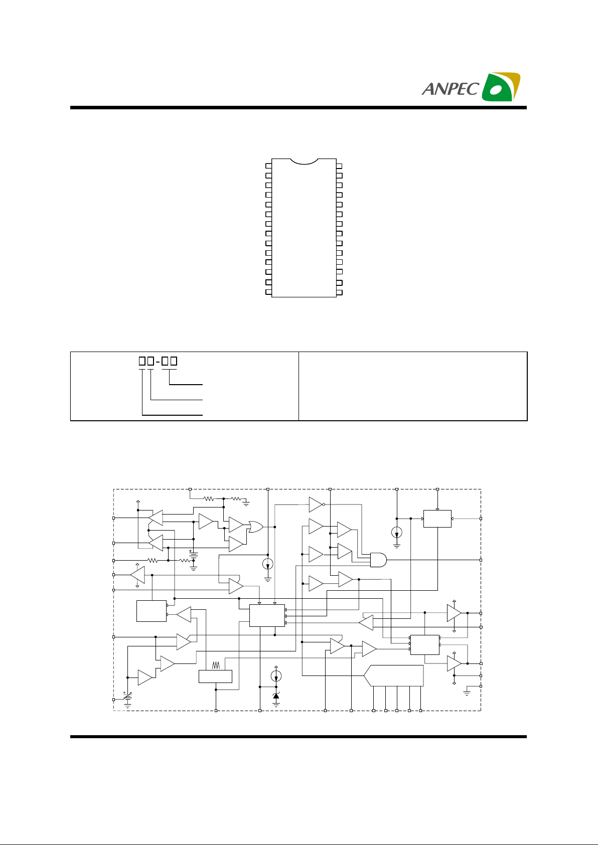
Pin Description
Ordering Information
APW6020
Package Code
K : SOP - 28
Temp. Range
C : 0 to 70 C
Handling Code
TU : Tube TR : Tape & Reel
°
Handling Code
Temp. Range
Package Code
Block Diagram
VCC
FAULT/ RT
1
2
3
4
5
6
7
8
OCSET2
12
11
10
9
SS
16
15
13
14
17
18
19
20
24
23
22
21
28
27
26
25
LGATE1
OCSET1
VSEN1
PGND
FB1
COMP1
UGATE1
PHASE1
DRIVE3
GND
VAUX
DRIVE4
VID4
VID3
VID0
VID1
VID2
UGATE2
PHASE2
PGOOD
VSEN2
SELECT
VSEN4
VSEN3
PGOOD
Power-on
Reset (POR)
VCC
200µA
×
1.10
SOFT START &
FAULT LOGIC
+
-
GATE
CONTROL
PWM
COMP1
SYNCH
DRIVE
OV
DACOUT
UGATE1
PHASE1
VCC
LGATE1
PGND
COMP1SS
OCSET1
VSEN1
ERROR
AMP1
PWM1
VCC
OC1
DRIVER1
VAUX
LUV
LINEAR
UNDER-
VOLTAGE
+
DRIVE3
DRIVE4
+
-
VID0
TTL D/A
CONVERTER
(DAC)
VID1VID2 VID3 VID4
+
-
1.26V
+
-
+
-
OSCILLATOR
FAULT/ RT
×
0.90
×
1.15
VCC
4.5V
28
µ
A
FAULT
INHIBIT
×
0.75
VCC
VSEN4
VSEN2
SELECT
GND
×
0.75
VSEN3
+
-
+
-
+
-
GATE
CONTROL
+
-
+
-
-
+
+
-
PHASE2
UGATE2
+
-
OCSET2
FB1
VCC
DRIVE2
INHIBIT
PWM2
PWM
COMP2
ERROR
AMP2
1.5V
or
3.3V
200
µ
A
Page 3
Copyright ANPEC Electronics Corp.
Rev. A.2 - May, 2001
APW6020
www.anpec.com.tw3
Absolute Maximum Ratings
Thermal Characteristics
Symbol Parameter Rating Unit
V
CC
Supply Voltage 15 V
VI , V
O
Input , Output or I/O Voltage GND -0.3 V to V
CC
V
T
A
Operating Ambient Temperature Range 0 to 70
°
C
T
J
Junction Temperature Range 0 to 125
°
C
T
STG
Storage Temperature Range -65 to +150
°
C
T
S
Soldering Temperature 300 ,10 seconds
°
C
Symbol Parameter Va lue Unit
R
θ
JA
Thermal Resistance in Free Air
SOIC
SOIC (with 3in
2
of Copper)
75
65
°
C/W
Electrical Characteristics
(Recommended operating conditions , Unless otherwise noted) Refer to Block and Simplified Power System
Diagrams , and Typical Application Schematic
APW6020
Symbol Parameter Test Conditions
Min. Typ. Max.
Unit
VCC Supply Current
I
CC
Nominal Supply Current UGATE1, LGATE1,
UGATE2, DRIVE3, and
DRIVE4 open
9mA
Power-on Reset
Rising VCC Threshold Vocset=4.5V 10.4 V
Falling VCC Threshold Vocset=4.5V 8.2 V
Rising VAUX Threshold Vocset=4.5V 2.5 V
VAUX Threshold Hysteresis Vocset=4.5V 0.5 V
Rising V
OCSET1
Threshold 1.26 V
Oscillator
F
OCS
Free Running Frequency RT= Open 185 200 215 kHz
∆
V
OSC
Ramp Amplitude RT= Open 1.9 V
P-P
DAC and Standard Buck Regulator Reference
DAC(VID0-VID4) Input Low
Voltage
0.8 V
Page 4
Copyright ANPEC Electronics Corp.
Rev. A.2 - May, 2001
APW6020
www.anpec.com.tw4
Electrical Characteristics Cont.
APW6020
Symbol Parameter Test Conditions
Min. T yp. Max.
Unit
DAC and Standard Buck Regulator Reference
DAC(VID0-VID4) Input High Voltage 2.0 V
DACOUT Voltage accuracy -1.0 +1.0 %
V
REG2
PWM2 Reference Voltage SELECT<0.8V 1.5 V
V
REG2
PWM2 Reference Voltage SELECT>2.0V 3.3 V
PWM2 Reference Voltage Tolerance 3 %
Linear Regulators (V
OUT3
and V
OUT4
)
Regulation (All Linears) 3 %
VREG3VSEN3 Regulation Voltage 1.5 V
VREG4VSEN4 Regulation Voltage 1.8 V
VSENUVUnder-Voltage Level (VSEN/ VREG) VSEN Rising 75 %
Under-Voltage Hysteresis (VSEN/ VREG) VSEN Falling 7 %
Output Drive Current (All Liners) V
DRIVE
=4.0V 20 40 mA
Synchronous PWM Controller Error Amplifier
DC Gain 88 dB
GBWP Gain-Bandwidth Product 15 MHz
SR Slew Rate COMP1=10pF 6
V/µs
PWM Controllers Gate Drivers
I
UGATE
UGATE1,2 Source VCC=12V, V
UGATE 1,2
=6V 1 A
R
UGATE
UGATE1,2 Sink V
UGATE1,2
=1V 3.5
Ω
I
LGATE
LGATE1 Source VCC=12V, V
LGATE 1
=1V 1 A
R
LGATE
LGATE1 Sink V
LGATE1
= 1V 3
Ω
Protection
VSEN1 Over-Voltage (VSEN1/DACOUT) VSEN1 Rising 115 120 %
I
OVP
FAULT Souring Current V
FAULT/RT
=2.0V 8.5 mA
I
OCSET
OCSET1,2 Current Source V
OCSET
= 4.5V
DC
170 200 230
µ
A
I
SS
Soft Sta rt Current 28
µ
A
Power Good
VSEN1 Upper Threshold
(VSEN1/DACOUT)
VSEN1 Rising
108 110 %
VSEN1 Under Voltage (V SE N 1/DACOUT)
VSEN1 Rising
92 94 %
VSEN1 Hysteresis
(VSEN1 DACOUT)
Upper /Lower Threshold 2 %
V
PGOOD
PGOOD Voltage Low I
PGOOD
= -4mA 0.8 V
Page 5

Copyright ANPEC Electronics Corp.
Rev. A.2 - May, 2001
APW6020
www.anpec.com.tw5
Functional Pin Description
UGATE2 (Pin 1)
Connect UGATE2 pin to the standard BUCK PWM
converter’s MOSFET gate. This pin provides the gate
drive for the MOSFET.
PHASE2 (Pin 2)
Connect the PHASE2 pin to the standard BUCK PWM
converter’s MOSFET source. This pin is used to
monitor the voltage drop across the MOSFET for
over-current protection.
VID0 , VID1 , VID2 , VID3 , VID4 (Pins 7, 6 , 5 , 4 and
3)
VID0-4 are the TTL-compatible input pins to the 5-bit
DAC. The logic states of these five pins program the
internal voltage reference (DACOUT). The level of
DACOUT sets the microprocessor core converter
output voltage , as well as the coresponding PGOOD
and OVP thresholds.
PGOOD (Pin 8)
PGOOD is an open drain output used to indicate the
status of the output voltages. This pin is pulled low
when the synchronous regulator output is not within
10% of the DACOUT reference voltage or when any
of the other outputs are below their under-voltage
thresholds.
The PGOOD output is open for ‘11111’ VID code.
OCSET2 (Pin 9)
Connect a resistor (R
OCSET
) from this pin to the drain
of the standard BUCK converter’s MOSFET. R
OCSET
,
an internal 200µA current source (I
OCSET
) , and the
MOSFET’s on-resistance(r
DS(ON)
) set the converter
over-current (OC) trip point according to the following equation :
I
PEAK
=
An over-current trip cycles the soft-start function.
VSEN2 (Pin 10)
Connect this pin to the output of the standard Buck
PWM converter. The voltage at this pin is regulated
to the level predetermined by the logic-level status of
the SELECT pin. This pin is also monitored by the
PGOOD comparator circuit.
SELECT (Pin 11)
This pin determines the output voltage of the AGP
bus switching regulator. A low TTL input sets the
output voltage to 1.5V , while a high input sets the
output voltage to 3.3V.
SS (Pin 12)
Connect a capacitor from this pin to ground. This
capacitor , along with an internal 28µA current source
, sets the soft-start interval of the converter.
FAULT / RT (Pin 13)
This pin provides oscillator switching frequency
adjustment. By placing a resistor (RT ) from this pin
to GND , the nominal 200kHz switching frequency is
increased. Conversely , connecting a pull-up resistor (RT ) from this pin to VCC reduces the switching
frequency.
Nominally , the voltage at this pin is 1.26V. In the
event of an over-voltage or over-current condition ,
this pin is internally pulled to VCC.
VSEN4 (Pin 14)
Connect this pin to the output of the linear 1.8V
regulator. This pin is monitored for under-voltage
events.
DRIVE4 (Pin 15)
Connect this pin to the gate of an external MOSFET.
This pin provides the drive for the 1.8V regulator’s
pass transistor.
VAUX (Pin 16)
The +3.3V input voltage at this pin is monitored for
I
OCSET
* R
OCSET
r
DS(ON)
Page 6

Copyright ANPEC Electronics Corp.
Rev. A.2 - May, 2001
APW6020
www.anpec.com.tw6
power-on reset (POR) purposes.
GND (Pin 17)
Signal ground for the IC. All voltage levels are measured with respect to this pin.
DRIVE3 (Pin 18)
Connect this pin to the gate of an external MOSFET.
This pin provides the drive for the 1.5V regulator’s
pass transistor.
VSEN3 (Pin 19)
Connect this pin to the output of the 1.5V linear
regulator. This pin is monitored for under-voltage
events.
COMP1 and FB1 (Pins 20 , and 21)
COMP1 and FB1 are the available external pins of
the synchronous PWM regulator error amplifier. The
FB1 pin is the inverting input of the error amplifier.
Similarly , the COMP1 pin is the error amplifier output.
These pins are used to compensate the voltage-mode
control feedback loop of the synchronous PWM
converter.
VSEN1 (Pin 22)
This pin is connected to the synchronous PWM
converters’s output voltage. The PGOOD and OVP
comparator circuits use this signal to report output
voltage status and for over-voltage protection.
OCSET1 (Pin 23)
Connect a resistor (R
OCSET
) from this pin to the drain
of the synchronous PWM converter’s upper MOSFET.
R
OCSET
, an internal 200µA current source (I
OCSET
) ,
and the MOSFET’s on-resistance(r
DS(ON)
) set the converter over-current (OC) trip point according to the
following equation :
I
PEAK
=
An over-current trip cycles the soft-start function. The
voltage at OCSET1 pin is monitored for power-on
reset (POR) purposes.
PGND (Pin 24)
This is the power ground connection. Tie the synchronous PWM converter’s lower MOSFET source
to this pin.
LGATE1 (Pin 25)
Connect LGATE1 to the synchronous PWM
converter’s lower MOSFET gate. This pin provides
the gate drive for the lower MOSFET.
PHASE1 (Pin 26)
Connect the PHASE1 pin to the synchronous PWM
converter’s upper MOSFET source. This pin is used
to monitor the voltage drop across the upper MOSFET
for over-current protection.
UGATE1 (Pin 27)
Connect UGATE1 pin to the synchronous PWM
converter’s upper MOSFET gate. This pin provides
the gate drive for the upper MOSFET.
VCC (Pin 28)
Provide a 12V bias supply for the IC to this pin. This
pin also provides the gate bias charge for all the
MOSFETs controlled by the IC. The voltage at this
pin is monitored for Power-On Reset (POR) purposes.
Functional Pin Description Cont.
I
OCSET
* R
OCSET
r
DS(ON)
Page 7

Copyright ANPEC Electronics Corp.
Rev. A.2 - May, 2001
APW6020
www.anpec.com.tw7
Simplified Power System Diagram
Table1 Output Voltage Program
NOTE : 0 = connected to GND , 1 = open or connected to 5V through pull-up resistors
Pin Name Pin Name
VID4 VID3 VID2 VID1 VID0
Nominal
DACOUT
Voltage
VID4 VID3 VID2 VID1 VID0
Nominal
DACOUT
Voltage
011111.30111110
011101.35111102.1
011011.40111012.2
011001.45111002.3
010111.50110112.4
010101.55110102.5
010011.60110012.6
010001.65110002.7
001111.70101112.8
001101.75101102.9
001011.80101013.0
001001.85101003.1
000111.90100113.2
000101.95100103.3
000012.00100013.4
000002.05100003.5
Standard
Buck
PWM
Controller
Synchronous
PWM
Controller
Linear
Controller
Linear
Controller
APW6020
V
OUT4
V
OUT1
Q1
Q2
Q3
Q4 Q5
V
OUT3
+5V
IN
+3.3V
IN
V
OUT2
Page 8

Copyright ANPEC Electronics Corp.
Rev. A.2 - May, 2001
APW6020
www.anpec.com.tw8
Typical Characteristics
Switching Frequency ( kHz )
1
10
100
1000
10000
50 150 250 350 450 550 650 750
RT ( kΩ )
Typical Characteristics
APW6020
OCSET2
UGATE2
PHASE2
VSEN2
SELECT
VAUX
DRIVE3
VSEN3
DRIVE4
VSEN4
SS
GND
VID4
VID3
VID2
VID1
VID0
FAULT/RT
COMP1
FB1
VSEN1
PGND
LGATE1
PHASE1
UGATE1
PGOOD
OCSET1
VCC
C
IN
3000µF
L
IN
1µH
Q3
CR1
L
OUT2
6.2
µ
H
Q4
Q5
V
OUT4
1.8V
V
OUT3
1.5V
+3.3V
IN
TYPEDET
V
OUT2
1.5V or 3.3V
+5V
IN
+12V
IN
C
OUT1
8000µF
L
OUT1
4.2
µ
H
V
OUT1
1.3V to 3.5V
POWERGOOD
Q1
Q2
C
4
1000pF
R
OCSET2
C
OUT2
3000
µ
F
C
1
1
µ
F
C
OUT3
1000µF
C
OUT4
1000µF
C
SS
0.1µF
C
3
1000pF
R
OCSET1
C
2
1
µ
F
R
4
10.2K
C
7
0.22µF
R
1
1.62K
C
5
10pF
C
6
2.7nF
R
2
150K
R
3
499K
RT pull down to GND
to +12V
RT pull up
Page 9

Copyright ANPEC Electronics Corp.
Rev. A.2 - May, 2001
APW6020
www.anpec.com.tw9
Typical Characteristics Cont.
DACOUT Voltage deviation (%)
Junction Temperature (oC) Junction Temperature (oC)
V
OUT2
Reference Voltage deviation (%)
V
OUT3
Reference Voltage deviation (%)
Junction Temperature (oC)
Junction Temperature (oC)
V
OUT4
Reference Voltage deviation (%)
Note : The Referance Voltage(V
REF
) Deviation is
V
REF(TJ
) - V
REF
(25oC)
V
REF
(25oC)
x 100%
-1.0 %
-0.8 %
-0.6 %
-0.4 %
-0.2 %
0.0%
0.2%
0.4%
0.6%
0.8%
1.0%
0102030405060708090100
-1. 0 %
-0. 8 %
-0. 6 %
-0. 4 %
-0. 2 %
0.0%
0.2%
0.4%
0.6%
0.8%
1.0%
0102030405060708090100
-1.0 %
-0.8 %
-0.6 %
-0.4 %
-0.2 %
0.0%
0.2%
0.4%
0.6%
0.8%
1.0%
0102030405060708090100
-1. 0 %
-0. 8 %
-0. 6 %
-0. 4 %
-0. 2 %
0.0%
0.2%
0.4%
0.6%
0.8%
1.0%
0102030405060708090100
TJ : Junction Temperature
Page 10

Copyright ANPEC Electronics Corp.
Rev. A.2 - May, 2001
APW6020
www.anpec.com.tw10
Package Information
SO – 300mil ( Reference JEDEC Registration MS-013)
Millimeters Variations- D Inches Variations- D
Dim
Min. Max. Variations Min. Max.
Dim
Min. Max. Variations Min. Max.
A2.35
2.65
SO-16
10.10 10.50
A 0.093 0.1043 SO-16 0.398 0.413
A1
0.10 0.30
SO-18
11.35 11.76
A1 0.004 0.0120 SO-18 0.447 0.463
B
0.33 0.51
SO-20
12.60 13
B 0.013 0.020 SO-20 0.496 0.512
D See variations SO-24
15.20 15.60
D See variations SO-24 0.599 0.614
E
7.40 7.60
SO-28
17.70 18.11
E 0.2914 0.2992 SO-28 0.697 0.713
e 1.27BSC SO-14
8.80 9.20
e 0.050BSC SO-14 0.347 0.362
H
10 10 .65
H 0.394 0.419
L
0.40 1.27
L 0.016 0.050
N See variations N See variations
φ
10°8
°φ
10°8
°
N
12
3
EH
D
L
GAUGE
PLANE
1
e
B
A1
A
Page 11

Copyright ANPEC Electronics Corp.
Rev. A.2 - May, 2001
APW6020
www.anpec.com.tw11
Classification Reflow Profiles
Package Reflow Conditions
Refolw Condition (IR/ Convection or VPR Reflow)
Physical Specifications
Terminal Material Solder-Plated Copper (Solder Material : 90/10 or 63/37 SnPb)
Lead Solderability Meets EIA Specification RSI86-91, ANSI/J-STD-002 Category 3.
Packaging 1000 devices per reel
Convection or IR/ Convection VPR
Average ramp-up rate(183°C to Peak) 3°C/second max. 10 °C /second max.
Preheat temperature 125 ± 25°C)
120 seconds max.
Temperature maintained above 183°C
60 ~ 150 seconds
Time within 5°C of actual peak
temperature
10 ~ 20 seconds 60 seconds
Peak temperature range
220 +5/-0°C or 235 +5/-0°C 215~ 219°C or 235 +5/-0°C
Ramp-down rate
6 °C /second max. 10 °C /second max.
Time 25°C to peak temperature
6 minutes max.
Reference JEDEC Standard J-STD-020A APRIL 1999
Pre-heat temperature
183 C
Peak temperature
Time
°
temperature
pkg. thickness ≥≥≥≥ 2.5mm
and all bags
pkg. thickness < 2.5mm and
pkg. volume ≥≥≥≥ 350 mm³
pkg. thickness < 2.5mm and pkg.
volume < 350mm³
Convection 220 +5/-0 °C Convection 235 +5/-0 °C
VPR 215-219 °C VPR 235 +5/-0 °C
IR/Convection 220 +5/-0 °C IR/Convection 235 +5/-0 °C
Page 12

Copyright ANPEC Electronics Corp.
Rev. A.2 - May, 2001
APW6020
www.anpec.com.tw12
Tape & Reel Dimensions
Reliability test program
Test item Method Description
SOLDERABILITY MIL-STD-883D-2003
245°C , 5 SEC
HOLT MIL-STD-883D-1005.7
1000 Hrs Bias @ 125 °C
PCT JESD-22-B, A102
168 Hrs, 100 % RH , 121°C
TST MIL-STD-883D-1011.9
-65°C ~ 150°C, 200 Cycles
ESD MIL-STD-883D-3015.7 VHBM > 2KV, VMM > 200V
Latch-Up JESD 78 10ms , Itr > 100mA
Application
A B C J T1 T2 W P E
SOP- 28
330±1 62 ±1.5 12.75 ± 0. 5 2 ± 0.6 24.4 ± 0.2 2± 0.2 24 ± 0.3 12 ± 0.1 1.75± 0.1
Application
F D D1 Po P1 Ao Bo Ko t
SOP- 28 11.5 ± 0.1
1.5 +0.1 1.5+ 0.25
4.0 ± 0.1 2.0 ± 0.1 10.85 ± 0.118.34± 0.1 2.97± 0.1 0.35±0.01
t
Ao
E
W
Po
P
Ko
Bo
D1
D
F
P1
A
J
B
T2
T1
C
Page 13

Copyright ANPEC Electronics Corp.
Rev. A.2 - May, 2001
APW6020
www.anpec.com.tw13
Cover Tape Dimensions
Customer Service
Carrier Width
24
Cover Tape Width
21.3
Anpec Electronics Corp.
Head Office :
5F, No. 2 Li-Hsin Road, SBIP,
Hsin-Chu, Taiwan, R.O.C.
Tel : 886-3-5642000
Fax : 886-3-5642050
Taipei Branch :
7F, No. 137, Lane 235, Pac Chiao Rd.,
Hsin Tien City, Taipei Hsien, Taiwan, R. O. C.
Tel : 886-2-89191368
Fax : 886-2-89191369
 Loading...