

Datasheet APW38HC43AJI-TR, APW38HC43AJC-TU, APW38HC43AJC-TR, APW38HC42AKI-TU, APW38HC42AKI-TR Datasheet (ANPEC)
...Page 1
APW38HC42A/3A/4A/5A
CMOS Current-Mode PWM Voltage Controller
Features General Description
Ultralow start-up current (25µA typical)
•
• Low operating current (2mA typical)
• Fast output rise/fall times :
−15ns rise/10ns fall
• High output drive (1.2A peak current)
• CMOS outputs with rail-to-rail swing
• Current-mode operation up to 1MHz
• Trimmed 5V bandgap reference
• Pin-to-pin compatible with MIC38HC4X
• Trimmed oscillator discharge current
• UVLO with hysteresis
• Low cross-conduction currents
The APW38HC4XA family are fixed frequency, high
performance, current-mode PWM controller with 1.2
A drive current capability. Undervoltage lockout circuitry allows the APW38HC42A and APW38HC44A
versions to start up at 14.5V and operate down to
9V, and the APW38HC43A and APW38HC45A versions start at 8.4V with operateion down to 7.6V. All
versions operate up to 24V. The ultra low start-up
current 25µA (typical), and operating current 2mA
(typical) have been designed to improve the converter
efficiency. High output driving capability up to 1.2A
ensures the fast switching to minimize the switching
losses. The APW38HC4XA features a trimmed and
temperature compensated oscillator discharge current and bandgap reference. APW38HC4XA is available in both 8-pin plastic DIP and SOP packages.
Applications
Current-mode , Off-line , Switched-mode Power
•
Supplies
• Current-mode , DC-to-DC converters
• Various converters ( step-down, step-up, flyback
, forward, and synchronous FET)
Pin Description
COMP
FB
ISNS
RT/CT
1
2
3
4
8
7
6
5
VREF
VDD
OUT
GND
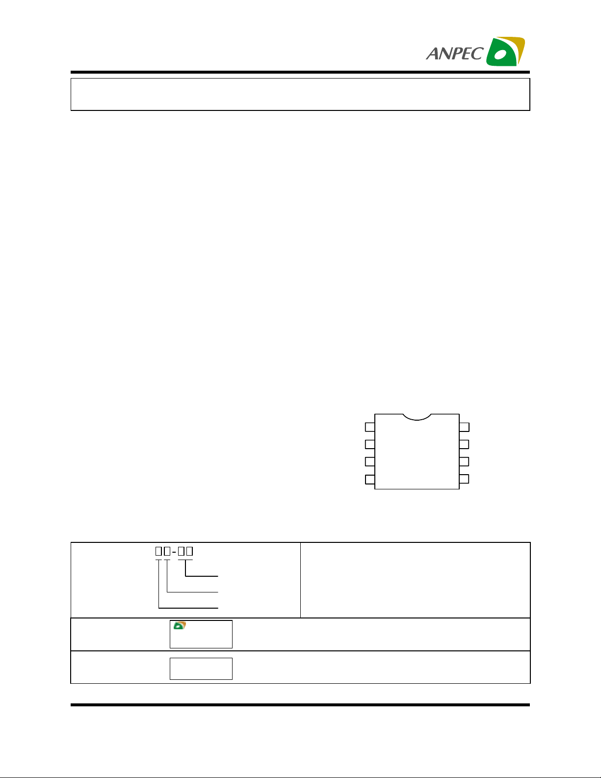
Ordering and Marking Information
APW38HC4XA
Handling Code
Temp. Range
Package Code
APW384XA J :
APW384XA K :
ANPEC reserves the right to make changes to improve reliability or manufacturability without notice, and advise
customers to obtain the latest version of relevant information to verify before placing orders.
APW38HC4XA
XXXXX
APW38HC4XA
XXXXX
Package Code
J : DIP - 8 K : SOP -8
Temp. Range
C : 0 to 70 C I : -40 to 85 C
Handling Code
TU : T u be TR : Tape & Reel
X - 2/3/4/5 XXXXX - Date Code
X - 2/3/4/5 XXXXX - Date Code
°
°
Copyright ANPEC Electronics Corp.
Rev. A.7 - Jan., 2003
www.anpec.com.tw1
Page 2
APW38HC42A/3A/4A/5A
Selection Guide
Duty Cycle
0~96% APW38HC43A APW38HC42A
0~50% APW38HC45A APW38HC44A
Block Diagram
VDD
VREF
RT/CT
FB
2.5V
-
E. A.
+
Startup 8.4V
Minimum Operating 7.6V
5V
Reference
Oscillator
2R
R
UVLO
-
+
T Q
S
R
Startup 14.5V
Minimum Operating 9V
Q
OUT
ISNSGNDCOMP
Functional Pin Description
Pin Name Pin Number Function Description
1 COMP Compensation: Connect external compensation network to
modify the error amplifier output.
2 FB Feedback (Input): Error amplifier input. Feedback is 2.5V at
desired output voltage.
3ISNS
4 RT/CT Timing Resistor/Timing Capacitor: Connect external RC
5 GND Ground: Combined analog and power ground.
6 OUT Power Output: Totem-pole output.
7VDD
8 VREF 5V Reference (Output): Connect external RC network.
Copyright ANPEC Electronics Corp.
Rev. A.7 - Jan., 2003
Current Sense (Input): Current sense comparator input.
Connect to current sensing resistor or current transformer.
network to select switching frequency.
Analog Supply (Input): Controller ci rcuitry supply input. Return
to analog ground (AGND).
www.anpec.com.tw2
Page 3
APW38HC42A/3A/4A/5A
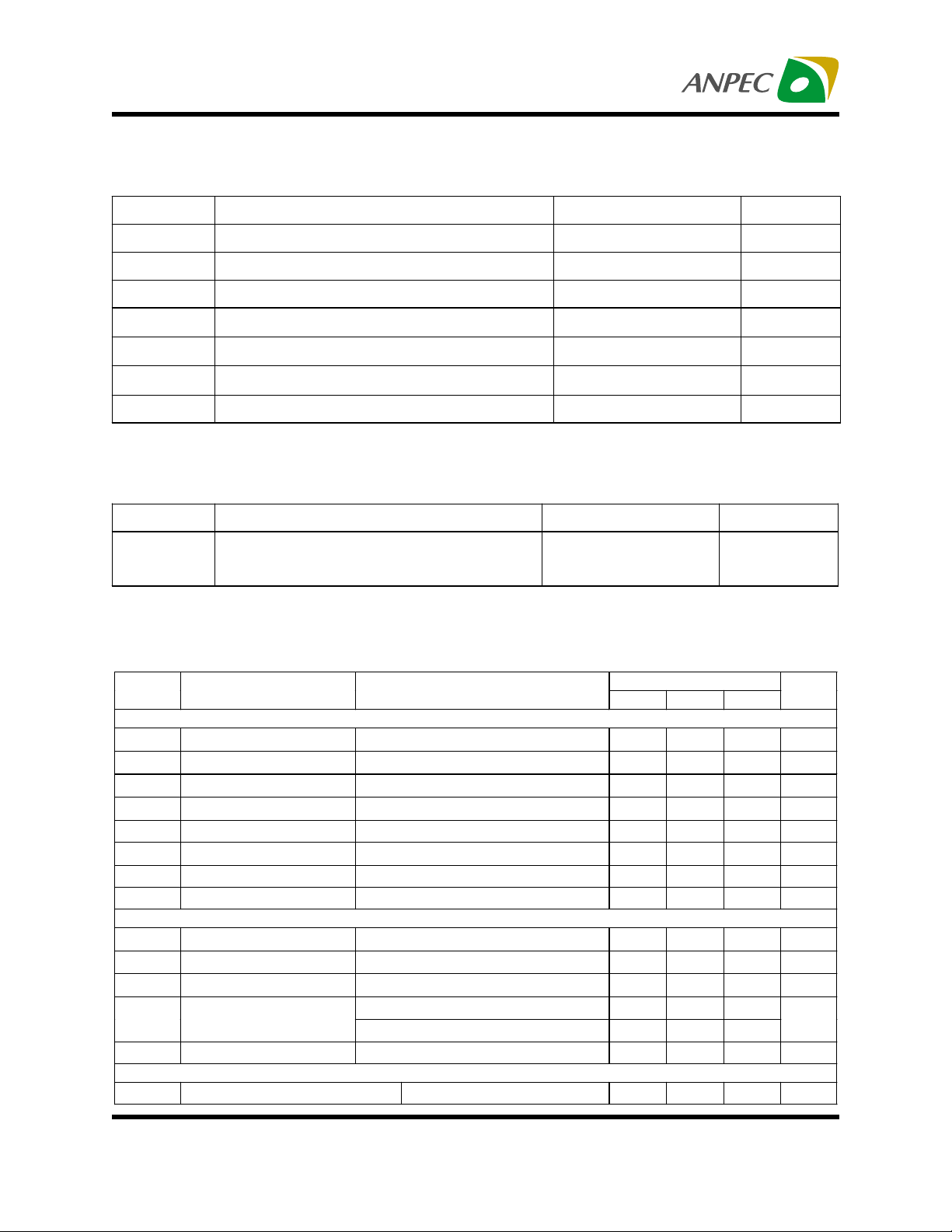
Absolute Maximum Ratings
Symbol Parameter Rating Unit
V
DD
V
ISNS
V
FB
T
J
T
STG
T
SDR
V
ESD
Supply Voltage 24 V
Current Sense Voltage -0.3 to 5.5 V
Feedback Voltage -0.3 to 5.5 V
Junction Temperature Range 300
Storage Temperature -65 to 150
Soldering Temperature 300,10 Seconds
Minimum ESD Rating ±3 kV
Thermal Characteristics
Symbol Parameter Value Unit
θ
JA
Thermal Resistance in Fr ee A ir
DIP
SOP
125
175
Electrical Characteristics
VDD =15V, Note3 ; RT=9.09KΩ; CT=3.3nF; -40oC ≤ TA ≤ 85oC; unless noted
Symbol Parameter Test Conditions
REFEREN CE VO LTA GE
V
REG
REG
Reference Voltage
REF
Line Regulation
line
Load Regulation
load
=25°C, IO(Output Current)=1mA
T
A
12V≤ V
1mA≤ I
DD
O
≤
18V, I
≤
20mA
=5µA
O
Te mp. S t a b i lity 0.2
Total Output Variation Line, Load, Temp. 4.82 5.18 V
Output Noise Voltage
10Hz≤ f ≤10kHz, T
= 25oC
A
Long Term Stability TA = 125oC, 1000 hrs 5 25 mV
I
SC
Output Short Circu it -25 -55 -120 mA
OSCILLATOR
F
I
DISCHG
V
Initial Ac curacy
OSC
Voltage Stability
Temp . Stability
Clock Ramp Reset
Current
Amplitude V
OSC
T
=25°C, Note 4
A
12V≤ V
T
≤ TA ≤ T
MIN
TA=25°C, V
T
A=TMIN
RT/CT
18V
DD
≤
MAX
=2V
RT/CT
to T
MAX
peak to peak 1.6 V
ERROR AMPLIFIER
Input Voltage V
=2.5V 2.42 2.50 2.5 8 V
COMP
APW38HC4XA
Min. Typ. Max.
4.90 5.00 5.10 V
120mV
625mV
50
49 52 55 kHz
0.2 1.0 %
0.03
7.7 8.4 9.0
7.2 8.4 9.5
C/W
°
C
°
C
°
C
°
Unit
mV/°C
V
µ
%/°C
mA
P-P
Copyright ANPEC Electronics Corp.
Rev. A.7 - Jan., 2003
www.anpec.com.tw3
Page 4
APW38HC42A/3A/4A/5A
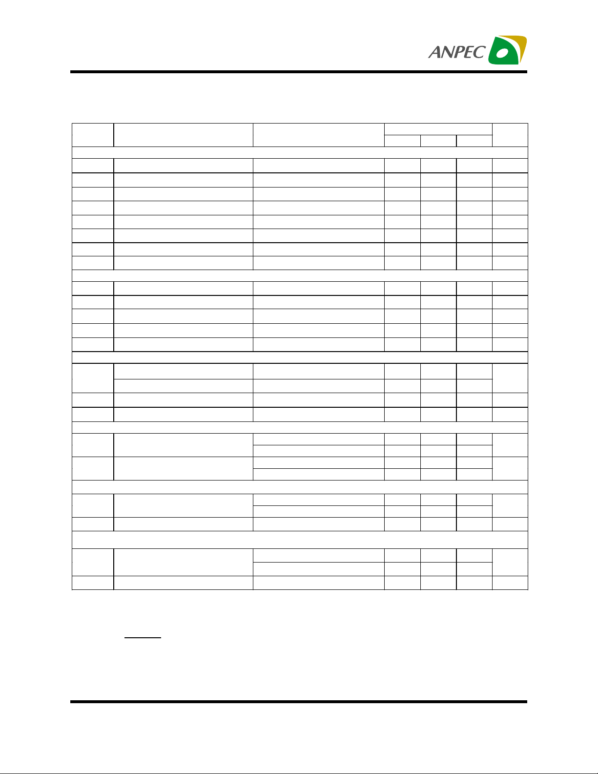
Electrical Characteristics (Cont.)
VDD =15V, Note3 ; RT=9.09KΩ; CT=3.3nF; -40oC ≤ TA ≤ 85oC; unless noted
Symbol Parameter Test Conditions
ERROR AMPLIFIER
I
Input Bias Current VFB=5V 0.1
FB
A
Open Loop Gain
VOL
2≤ V
4V
O
≤
BW Unit y Gain Band widt h 0.7 1. 0 MH z
PSRR
Output Sink Current VFB=2.7V, V
Output Source Current VFB=2.3V, V
V
V
Output Voltage (High) VFB=2.3V, RL=15k to GND 5 5.4 V
OH
Output Voltage (Low) VFB=2.7V, RL=15k to VREF 0.01 1.1 V
OL
12≤ V
DD
≤
18V
COMP
COMP
=1.1V 2 7 mA
=5V -0.5 -1 mA
CURRENT SENSE
A Gain Notes 1,2 2.85 3.0 3.15 V/V
V
I
Maximum Threshold V
THM
PSRR
Input Bias Current V
ISNS
T
Delay to Output 120 250 ns
D
=5V, Note 1 0.9 1.0 1.1 V
COMP
12≤ V
ISNS
18V, Note 1
DD
≤
=5V 0.1
OUTPUT
t
R
t
F
R
R
Rise Time
Fall Time
High Sourcing Current = 200mA 6.3
DS(ON)
Low Sinking Current = 200mA 4
DS(ON)
T
=25°C, CL=1nF
A
T
=25°C, CL=1nF
A
UNDERVOLTAGE LOCKOUT
V
DD(ST)
V
DD(MIN)
Start Threshold
Minimum Operating Voltage
APW38H C42 /4A 13.5 14.5 15.5
APW38HC43/5A 7.8 8.4 9.0
APW38HC42/4A 8.0 9.0 10.0
APW38HC43/5A 7.0 7.6 8.2
PULSE WIDTH MODULATOR
D
D
Maximum Duty Cycle
MAX
Min imum Du ty Cy c le 0
MIN
APW38HC42/3A 94 96
APW38HC44/5A 46 50
TOTAL STANDBY CURRENT
I
DD(ST)
I
DD(OP)
Start-Up Current
Operating Supply Current VFB =V
VDD=13V, A PW38HC42/4A 30 150
V
=7.5V, APW38HC43 /5A 25 150
DD
= 0V, CL=1nF 2.0 4.0 mA
ISNS
Note 1 : Parameter measured at trip point of latch with VFB=0V.
Note 2 : Gain defined as :
APW38H C4X A
Min. Typ. Max.
60 70 dB
60 dB
70 dB
15 30 ns
10 20 ns
Unit
A
µ
A
µ
Ω
V
V
%
%
A
µ
A = , 0<VTH(ISNS)<0.8V
∆VCOMP
∆VTH(ISNS)
Note 3 : Adjust VDD above the start threshold before setting at 15V.
Note 4 : Output frequency equals oscillator frequency for the APW38HC42A and APW38HC43A. Output
frequency for APW38HC44A and APW38HC45A equals one half of the oscillator frequency.
Copyright ANPEC Electronics Corp.
Rev. A.7 - Jan., 2003
www.anpec.com.tw4
Page 5

APW38HC42A/3A/4A/5A
Typical Characteristics
Oscillator Frequency Configuration
100
200
pF
470
pF
1
nF
10
1.8
nF
4.7
nF
10
nF
RT Resistance (kΩ)
1
10 100 1000
Oscillator Frequency (kHz)
Oscillator Discharge Current vs.
Temperature
9.0
8.8
8.6
8.4
8.2
8.0
7.8
7.6
7.4
7.2
Oscillator Discharge Current (mA)
7.0
-60-30 0 30 6090120150
VDD = 15V
VRTCT = 2V
Output Dead Time vs. Oscillator Frequency
100
10nF
4.7nF
10
Output Dead Time ( %)
1.8nF
200pF
470pF
1nF
1
10 100 1000
Oscillator Frequency (kHz)
Current Sense Amplifier Threshold vs.
Error Amplifier Output
1.2
1.0
0.8
0.6
0.4
0.2
Current Sense AMP Threshold (V)
0.0
01234567
-50oC
25oC
125oC
Temperature (°C)
Copyright ANPEC Electronics Corp.
Rev. A.7 - Jan., 2003
Error Amplifier Output (V)
www.anpec.com.tw5
Page 6

APW38HC42A/3A/4A/5A
Typical Characteristics (Cont.)
Short-Circuit Current of VREF vs.
Temperature
100
90
80
70
60
50
40
30
20
10
VREF Short-Circuit Current (mA)
0
-60 -30 0 30 60 90 120 150
Output Waveform
30
25
20
15
10
5
0
Output Voltage (V)
-5
-10
0.0 0.1 0.2 0.3 0.4 0.5 0.6 0.7 0.8
Temperature (°C)
Open Loop test Circuit
R
4.7KΩ
1K
Error A m p
Adjust
4.7KΩ
Ω
2N2222
100KΩ
5KΩ
SENSE
I
Adjust
T
COMP
APW38HC42A/3A/4A/5A
VFB
ISENSE
RT/CT
C
T
REF
Vcc
OUTPUT
GND
0.1µF
A
1KΩ,1W0.1µF
Time (µs)
REF
Vcc
Output
GND
Copyright ANPEC Electronics Corp.
Rev. A.7 - Jan., 2003
www.anpec.com.tw6
Page 7

APW38HC42A/3A/4A/5A
Packaging Information
PDIP-8 pin ( Reference JEDEC Registration MS-001)
D
Dim
A
A1
A2
L
e1
e2
e3
E
E1
E3
L
∅
E1
1
A
L
A1
e2
e 1
e 3
Millimeters Inches
Min. Max. Min. Max.
5.33 0.210
0.38 0.015
2.92 3.68 0.115 0.145
9.02 10.16 0.355 0.400
2.54BSC 0.100BSC
0.36 0.56 0.014 0.022
1.14 1.78 0.045 0.070
7.62 BSC
8.26
6.10 7.11 0.240 0.280
10.92 0.430
2.92 3.81 0.115 0.150
10°15
E
A2
1
E3
0.300 BSC
0.325
°
0
°
15
°
Copyright ANPEC Electronics Corp.
Rev. A.7 - Jan., 2003
www.anpec.com.tw7
Page 8

APW38HC42A/3A/4A/5A
Package Information
SOP- 8 pin ( Reference JEDEC Registration MS-012)
e1 e2
D
0.004max.
A1
0.015X45
HE
A
°°°°
e
1
L
Dim
A 1.35 1.75 0.053 0.069
A1 0.10 0.25 0.004 0.010
D 4.80 5.00 0.189 0.197
E 3.80 4.00 0.150 0.157
H 5.80 6.20 0.228 0.244
L 0.40 1.27 0.016 0.050
e1 0.33 0.51 0.013 0.020
e2 1.27BSC 0.50BSC
18
∅
Copyright ANPEC Electronics Corp.
Rev. A.7 - Jan., 2003
Millimeters Inches
Min. Max . Min. Max.
°
8
°
www.anpec.com.tw8
Page 9

APW38HC42A/3A/4A/5A
Physical Specifications
Termina l Mater ial Solder-Plated Cop p er (S o lder Material : 90/10 or 63/37 Sn Pb)
Lead Solderab ility Meets E IA Specification RSI86-91, ANSI/J-STD-002 C ategory 3.
Reflow Condition (IR/Convection or VPR Reflow)
Reference JEDEC Standard J-STD-020A APRIL 1999
Peak temperature
temperature
Pre-heat temperature
°
183 C
Time
Classificatio n R e flow Profiles
Convection or IR/
Convection
Average ramp-up rate(183°C to Peak) 3°C/second max. 10 °C /second max.
Preheat temperature 125 ± 25°C)
Temperature maintained above 183°C
Time within 5°C of actual peak temperature
Peak temperature range
Ramp-down rate
Time 25°C to peak temperature
120 seconds max
60 – 150 seconds
10 –20 seconds 60 seconds
220 +5/-0°C or 235 +5/-0°C 215-219°C or 235 +5/-0°C
6 °C /second max. 10 °C /second max.
6 minutes max.
VPR
Package Reflow Conditions
pkg. thickness ≥≥≥≥ 2.5mm
and all bgas
Convection 220 +5/-0 °C Convection 235 +5/-0 °C
VPR 215-219 °C VPR 235 +5/-0 °C
IR/Convection 220 +5/-0 °C IR/Convection 235 +5/-0 °C
Copyright ANPEC Electronics Corp.
Rev. A.7 - Jan., 2003
pkg. thickness < 2.5mm and
pkg. volume ≥≥≥≥ 350 mm³
pkg. thickness < 2.5mm and p kg .
volume < 350mm³
www.anpec.com.tw9
Page 10

APW38HC42A/3A/4A/5A
Re lia b i li ty test prog r am
Test item Method Description
SOLDERABILITY MIL-STD-883D-2003
HOLT MIL-STD-883D-1005.7
PCT JESD-22-B, A102
TST MIL-STD-883D-1011.9
ESD MIL-STD-883D-3015.7 VHBM > 2KV, VMM > 200V
Latch-Up JESD 78 10ms , Itr > 100mA
Carrier Tape & Reel Dimensions
245°C , 5 SEC
1000 Hrs Bias @ 125 °C
168 Hrs, 100 % RH , 121°C
-65°C ~ 150°C, 200 C y c les
t
E
Po
F
W
A
P
P1
Ao
J
D
Bo
Ko
D1
T2
C
B
Application
SOP-8
Application
SOP-8
Copyright ANPEC Electronics Corp.
Rev. A.7 - Jan., 2003
A B C J T1 T2 W P E
330±162 ± 1.5 12.75 +
F D D1 Po P1 Ao Bo Ko t
5.5 ± 0.1 1.55±0.1 1.5+ 0.25 4.0 ± 0.1 2.0 ± 0.1 6.4 ± 0.1 5.2± 0.1 2.1± 0.1 0.3±0.013
0.1 5
T1
2 + 0.5 12.4 +0.2 2± 0.2 12 + 0.3
- 0.1
8± 0.1 1.75± 0.1
(mm)
www.anpec.com.tw10
Page 11

APW38HC42A/3A/4A/5A
Cover Tape Dimensions
Application Carrier Width Cover Tape Width Devices Per Reel
SOP- 8
Customer Service
Anpec Electronics Corp.
Head Office :
5F, No. 2 Li-Hsin Road, SBIP,
Hsin-Chu, Taiwan, R.O.C.
Tel : 886-3-5642000
Fax : 886-3-5642050
Taipei Branch :
7F, No. 137, Lane 235, Pac Chiao Rd.,
Hsin Tien City, Taipei Hsien, Taiwan, R. O. C.
Tel : 886-2-89191368
Fax : 886-2-89191369
12 9.3 2500
Copyright ANPEC Electronics Corp.
Rev. A.7 - Jan., 2003
www.anpec.com.tw11
 Loading...