

Page 1
APW1175
Dual Synchronous DC/DC Controllers with Current Sharing Control
Features
• Two Operation Modes
- Independent Operation
- Two-Phase Operation with Current Sharing
• Driving N-Channel MOSFETs
•
300kHz Constant Frequency Operation
• Built-in Feedback Compensation
- Voltage-Mode PWM Control
- Fast Transient Response
• ±1% VREF Accuracy Over Temperature
•
Adjustable Output Voltage by an External Resistor
Divider
• Phase-Shifted Switchers to Minimize Ripple
• Current Limit with 50% Fold-Back
•
Soft-Start and Enable Function
••
• Power-ON Reset (POR) Monitor
••
••
• Power Good Monitor for Outputs
••
General Description
The APW1175 is a two-phase, synchronous, and voltage
mode PWM controller to provide dual channel or single
outputs in two distinct operation modes. In independent
mode, the two PWM converters supply two independently
regulated voltages by converting a common or two differ-
ent power inputs. In two-phase mode, the two PWM con-
verters supply one regulated voltage with programmable
current sharing control by converting a common or two
different power inputs. The two-phase mode can supply
the larger power than that provided each single channel.
APW1175 features an internal 300KHz oscillator, VCC
Power-On-Reset (POR), an external adjustable soft-start
and the programmable output current limit with 50% fold-
o
back. The two PWM controllers are 180
out of phase to
minimize the input ripple (common power input) and the
output ripple (two-phase mode).
Pin Description
Applications
••
• Graphics Cards
••
••
• DDR Memory
••
••
• SSTL-2 Termination
••
••
• Power Supply Requiring Two Outputs
••
VREF
+IN 2
-IN 2
VCC
CL2-
CL2+
BST2
DH2
DL2
PGND
1
2
3
4
5
6
7
8
9
10
20
19
18
17
16
15
14
13
12
11
GND
PWR G D
-IN 1
SS/ENA
CL1-
CL1+
BST1
DH1
DL1
BSTC
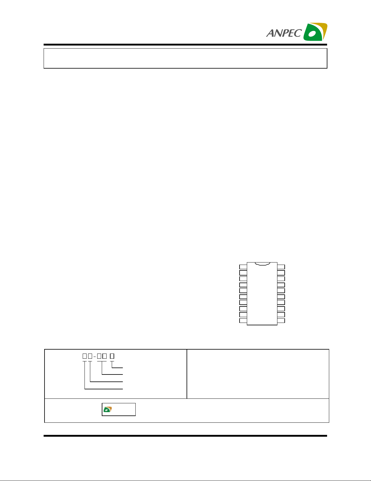
Ordering and Marking Information
)29 %#
Lead Free Code
Handling Code
Temp. Range
Package Code
APW 1175 K :
ANPEC reserves the right to make changes to improve reliability or manufacturability without notice, and advise
customers to obtain the latest version of relevant information to verify before placing orders.
Copyright ANPEC Electronics Corp.
Rev. A.3 - July., 2003
APW 1175
XXXXX
Package Code
K : SOP -20
Temp. Range
C : 0 to 70°C
Handling Code
TU : Tube TR : Tap e & Reel
Lead Free Code
L : Lead Free Device Blank : Orginal Device
XXXXX - Date Code
www.anpec.com.tw1
Page 2
APW1175
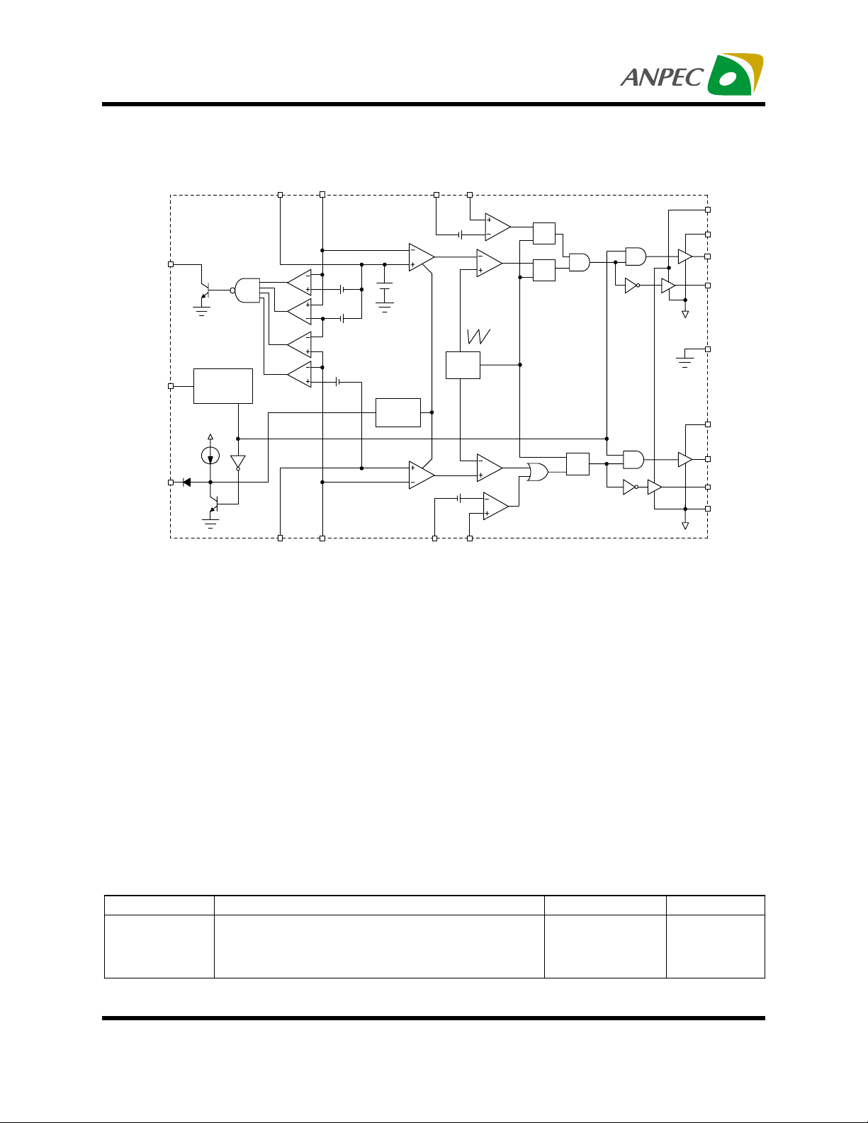
Block Diagram
VR EF -IN1 CL1- CL1+
PWRGD
VCC
SS/ENA
25uA
POWER-ON
RESET(POR)
4V
+IN2
-IN2
0.125V
0.125V
0.125V
Master Error
Am plifier
V REF
1.25V
soft-start
control
Slave Error
Am plifier
V CL1
OSC
V
CL2
CL2- CL2+
300KHZ
R
Q
S
R
Q
S
S
Q
R
Absolute Maximum Ratings Operating Conditions
BSTC
BST1
DH1
DL1
GND
BST2
DH2
DL2
PGND
••
• VCC to GND . . . . . . . . . . . . . -0.3V ~ 15V
••
••
• PGND to GND . . . . . . . . . . . . ±1V
••
••
• BST to GND . . . . . . . . . . . . . -0.3V ~ 22V
••
••
• Junction Temperature . . . . . . . 150
••
••
• Storage Temperature . . . . . . . -65
••
••
• Soldering Temperature . . . 300
••
••
• Minimum ESD Rating . . . . . . . ±3kV
••
o
C
o
C ~ 150oC
o
C , 10 Seconds
Thermal Characteristics
Symbol
R
JA
Copyright ANPEC Electronics Corp.
Rev. A.3 - July., 2003
Thermal Resistance in Free Air
Parameter Rating Unit
SOIC
SOIC(with 3in
••
• VCC . . . . . . . . . . . . . . . . . . . . 4.2V ~ 15V
••
••
• BST. . . . . . . . . . . . . . . . . . . . . 5V ~ 17V
••
www.anpec.com.tw2
o
C to 85oC
o
C to 125oC
C/W
°
••
• Ambient Temperature Range . . . 0
••
••
• Junction Temperature Range. . . . 0
••
75
of Copper)
65
Page 3
APW1175
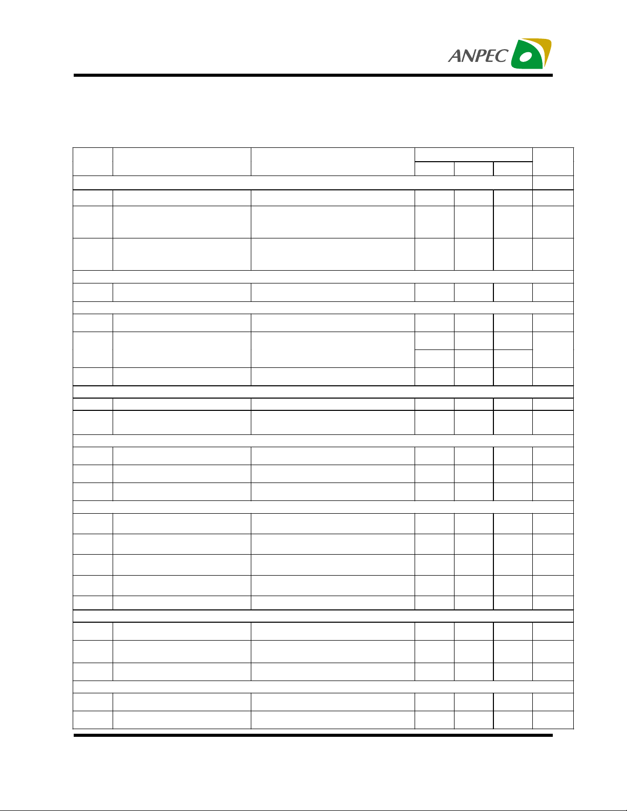
Electrical Characteristics
Unless otherwise specified, these specifications apply over VCC=4.75~5.25V, GND=PGND=0V, and T)=0~85°C.
Typical values refer to T
Symbol Parameter Test Conditions
SUPPLY CURRENT
ICC V
BSTC
I
BST1,2
I
CC
Supply Current
BSTC Supply Current
BST1,2 Supply Current
POWER-ON RESET
CC
POR Threshold Voltage VCC Rising 3.6 4.2 V
V
OSCILLATOR
OSC
F
O s c illator F requency
Maxim um Duty C ycle
Ramp Amplitude
∆V
OSC
ERROR AMPLIFIER
AOL Error Amplifier Voltage Gain 35 dB
REFERENCE VOLTAGE
V
Reference Voltage Measure Pin 1 1.238 1.250 1.262 V
REF
REF
Load Regulation I
V
REF
Line Regulation VCC = 5~15V
V
PWM CONTROLLERS GATE DRIVERS
DH Source
DH Sink
DL Source
DL Sink
Dead Time 50 200 nS
CURRENT LIMIT PROTECTION
VCL
Current Limit Voltage 60 70 80 mV
SOFT-START
ISS
Soft-S tart C urrent V
Soft-Start Transition Synchronous PW M 3.3 V
Copyright ANPEC Electronics Corp.
Rev. A.3 - July., 2003
)=25°C.
CC
V
=5~15V, F
BSTC=5V, DL1,2=Open,
OSC
=300kHz
F
BST1,2=10V, DH1,2=Open,
OSC
=300kHz
F
Input Bias Current
(-IN1, +IN2, -IN 2)
Input Voltage = 1.25V
REF
= 1m A
BSTH-DH=5V
BSTH-DH=2.5V
DH-PGND=3.5V
DH-PGND=1.75V
BSTL-DL=5V
BSTL-DL=2.5V
DL-PGND=3.5V
DL-PGND=1.75V
OUT
=0V (refer to application
Fold Back Current
V
circuit)
Fold Back Voltage Knee I=I
SS
=1V 25
APW1175
Min Typ Max
OSC
=300kHz
9 mA
2.8
1.6
270 300 330 KHz
DH1
DH2
80 90
100
1.1 V
0.5 1
3.5
1
0.5
1
0.5
1
0.5
1
0.5
50% I
LIM
(refer to application circuit) 1.25 V
www.anpec.com.tw3
0.5 %
OUT
V
Unit
mA
mA
%
µA
mV
A
A
A
A
LIM
µA
Page 4

APW1175
Electrical Characteristics Cont.
Symbol Parameter Test Conditions
POWER GOOD
Upper -IN1 Threshold
APW1175
Min Typ Max
110%
Unit
V
REF
Lower IN1 Threshold
Upper IN2 Threshold
Lower IN2 Threshold
PWRGD Voltage Low I
=-5mA 0.8 V
PWRGD
Functional Pin Description
VREF (Pin 1)
Internal 1.25V reference voltage . This pin is internally
connected to the positive input of the master channel
error amplifier.
+IN2 (Pin 2)
Positive input of the slave channel error amplifier. Con-
nect this pin to 1.25V reference (Pin 1) for the two
independent channel configuration.
-IN2, -IN1 (Pin 3, 18)
Negative inputs of the slave and master error amplifier.
VCC (Pin 4)
Connect this pin to 5V~15 V power to provides the
bias for the control circuitry. Need a 1uF multi-layer
ceramic decoupling capacitor to GND (Pin 20). The
voltage at this pin is also monitored for Power-On
Reset (POR) purpose.
CL2-, CL2+, CL1+, CL1- (Pin 5,6,15,16)
Current sense input pins. Connect the positive and
negative inputs to output current sense resistor for
each channel. A current limit comparator for each
channel to limit the output current while the difference
voltage between the positive and negaive inputs is
greater than the 75mV reference.
A RC filter is required for noise rejection.
BST2,BST1 (Pin 7,14)
Power inputs to the high-side MOSFET drivers. A boot-
strap circuit may be used to pump a boot voltage .
90%
V
+IN2
+0.1V
REF
90%
DH2, DH1 (Pin 8,13)
High-side MOSFET drivers to provide strong drive current
to drive each high-side MOSFET. A small series resistor
to the gate of the MOSFET maybe required for each pin.
DL2, DL1 (Pin 9,12)
Low-side MOSFET drivers to provide strong drive current
to drive each low-side MOSFET. A small series resistor
to the gate of the MOSFET maybe required for each pin.
PGND (Pin 10)
Power ground connection. The pin provide the path for
return of gate drive currents.
BSTC (Pin 11)
This pin provide supply voltage to the low-side MOSFET
drivers.
SS/ENA (Pin 17)
Connect a capacitor from this pin to ground.This
capacitor, along with an internal 25uA current source,
sets the soft-start interval, preventing the outputs from
overshoot as well as limiting the input current. Pull this
pin to below 1.4V to shutdown the outputs
PWRGD (Pin 19)
Power good signal output pin. This pin is an open collec-
tor output, which is pulled low if the output voltage is out-
side the power good window.
GND (Pin 20)
Signal ground for the control circuitry. All voltage levels
are measured with respect to this pin.
V
REF
V
V
REF
Copyright ANPEC Electronics Corp.
Rev. A.3 - July., 2003
www.anpec.com.tw4
Page 5

APW1175
Typical Application
1. Independent Operation
16V
16V
16V
+12V
100uF
C1
100uF
C2
100uF
C3
APM4416
Q1
1uF
C5
+5V
150uF
C18
6V
150uF
C19
6V
150uF
C20
6V
R13
2.2
1N4148
D2
APM4416
Q3
R14
2.2
R15
2.2
1uF
C21
1nF
1uF
C22
C23
VREF
+IN2
-IN2
VCC
CL2CL2+
BST2
DH2
DL2
PGND
10nF
C11
GND
PWR GD
-IN1
SS/ENA
CL1CL1+
BST1
DH1
DL1
BSTC
PWR OK
10nF
C6
+5V
R2
2.2
0.22uF
C4
2.2
R1
2.2
1N4148
D1
R3
2.2
R4
APM4416
Q4
4.7uH
L2
150uF
6V
150uF
6V
150uF
6V
Copyright ANPEC Electronics Corp.
Rev. A.3 - July., 2003
100
6m
10nF
R11
R12
C15
C16
C17
C8
10nF
C9
124
0.22uF
C7
R7
6V
6V
6V
0.22uF
C10
124
R8
220
R9
R10
100
1.8V / 6A
100
R5
6m
R6
150uF
C12
150uF
C13
150uF
C14
2.5V / 6A
APM4416
7.5uH
Q2
L1
www.anpec.com.tw5
Page 6

APW1175
Typical Application
2. Two-Phase Operation with Current Sharing Control
+5V
150uF
C12
6V
150uF
C13
6V
150uF
C14
6V
R12
2.2
1N4148
D2
APM4416
Q3
R13
2.2
R14
2.2
C18
1uF
C15
1uF
C16
1nF
10nF
C17
22k
VREF
+IN2
-IN2
VCC
CL2CL2+
BST2
DH2
DL2
PGND
R11
GND
PWRGD
-IN1
SS/ENA
CL1CL1+
BST1
DH1
DL1
BSTC
PWRO K
10nF
+5V
R2
2.2
0.22uF
C4
2.2
C6
R1
2.2
1N4148
D1
R3
2.2
R4
+12V
100uF
16V
C1
100uF
16V
C2
100uF
16V
C3
APM4416
Q1
1uF
C5
APM4416
Q4
4.7uH
L2
Copyright ANPEC Electronics Corp.
Rev. A.3 - July., 2003
100
100
R9
10nF
C8
124
R8
R10
6m
0.22uF
C7
150
R7
150uF
6V
150uF
6V
150uF
6V
R5
6m
R6
C9
C10
C11
APM4416
Q2
7.5uH
L1
2.7V / 12A
www.anpec.com.tw6
Page 7

APW1175
Packaging Information
SO 300mil ( Reference JEDEC Registration MS-013)
D
N
EH
12
3
GAUGE
PLANE
A
e
Millimeters Variations- D Inches Variations- D
Dim
A1
φ
Min. Max. Variations Min. Max.
A2.35
0.10 0.30
0.33 0.51
B
D See variations SO-24
7.40 7.60
E
e 1.27BSC SO-14
H
L
N See variations N See variations
1 0
10 10.65
0.40 1.27
°
2.65
8
B
SO-16
SO-18
SO-20
SO-28
°φ
A1
10.10 10.50
11. 35 11. 76
12.60 13
15.20 15.60
17.70 18.11
8.80 9.20
Dim
A1 0.004 0.0120 SO-18 0.447 0.463
Min. Max. Variations Min. Max.
A 0.093 0.1043 SO-16 0.398 0.413
B 0.013 0.020 SO-20 0.496 0.512
D See variations SO-24 0.599 0.614
E 0.2914 0.2992 SO-28 0.697 0.713
e 0.050BSC SO-14 0.347 0.362
H 0.394 0.419
L 0.016 0.050
10°8
L
°
1
Copyright ANPEC Electronics Corp.
Rev. A.3 - July., 2003
www.anpec.com.tw7
Page 8

APW1175
Physical Specifications
Terminal Material Solder-Plated Copper (Solder Material : 90/10 or 63/37 SnPb)
Lead Solderability Meets EIA Specification RSI86-91, ANSI/J-STD-002 Category 3.
Reflow Condition (IR/Convection or VPR Reflow)
Reference JEDEC Standard J-STD-020A APRIL 1999
Peak temperature
temperature
Pre-heat temperature
°
183 C
Time
Classification Reflow Prof iles
Convection or IR/
Convection
Average ramp-up rate(183°C to Peak) 3°C/second max. 10 °C /second max.
Preheat temperature 125 ± 25°C)
Temperature maintained above 183°C
Time within 5°C of actual peak temperature
Peak temperature range
Ramp-down rate
Time 25°C to peak temperature
120 seconds max
60 150 seconds
10 20 seconds 60 seconds
220 +5/-0°C or 235 +5/-0°C 215-219°C or 235 +5/-0°C
6 °C /second max. 10 °C /second max.
6 minutes max.
VPR
Package Reflow Conditions
pkg. thickness
and all bgas
Convection 220 +5/-0 °C Convection 235 +5/-0 °C
VPR 215-219 °C VPR 235 +5/-0 °C
IR/Convection 220 +5/-0 °C IR/Convection 235 +5/-0 °C
Copyright ANPEC Electronics Corp.
Rev. A.3 - July., 2003
2.5mm
≥≥≥≥
pkg. thickness < 2.5mm and
pkg. volume
350 mm³
≥≥≥≥
pkg. thickness < 2.5mm and pkg.
volume < 350mm³
www.anpec.com.tw8
Page 9

APW1175
Re lia bility test program
Test item Method Description
SOLDERABILITY MIL-STD-883D-2003
HOLT MIL-STD-883D-1005.7
PCT JESD-22-B, A102
TST MIL-STD-883D-1011.9
ESD MIL-STD-883D-3015.7 VHBM > 2KV, VMM > 200V
Latch-Up JESD 78 10ms , IJH > 100mA
245°C , 5 SEC
1000 Hrs Bias @ 125 °C
168 Hrs, 100 % RH , 121°C
-65°C ~ 150°C, 200 Cycles
Carrier Tape
W
t
E
F
A
Po
P
P1
Ao
J
C
D
Bo
Ko
D1
T2
B
Application
A B C J T1 T2 W P E
330±1 62 ±1.5
SOP- 20
F D D1 Po P1 Ao Bo Ko t
11.5 ± 0.1 1.5 +0.1 1.5+ 0.25 4.0 ± 0.1 2.0 ± 0.1 8.2 ± 0.1 13± 0.1 2.5± 0.1
Copyright ANPEC Electronics Corp.
Rev. A.3 - July., 2003
12.75 +
0.15
T1
2 + 0.6 24.4 + 0.2 2 ± 0.2
24 + 0.3
-0.1
12 + 0.1 1.75± 0.1
.35±0.01
3
www.anpec.com.tw9
Page 10

APW1175
Cover Tape Dimensions
Application Carrier Width Cover Tape Width Devices Per Reel
SOP- 20
Customer Service
Anpec Electronics Corp.
Head Office :
5F, No. 2 Li-Hsin Road, SBIP,
Hsin-Chu, Taiwan, R.O.C.
Tel : 886-3-5642000
Fax : 886-3-5642050
Taipei Branch :
7F, No. 137, Lane 235, Pac Chiao Rd.,
Hsin Tien City, Taipei Hsien, Taiwan, R. O. C.
Tel : 886-2-89191368
Fax : 886-2-89191369
24 21.3 1000
Copyright ANPEC Electronics Corp.
Rev. A.3 - July., 2003
www.anpec.com.tw10
 Loading...