

Datasheet APV2002YI-W, APV2002YI-TY, APV2002YI-TU, APV2002YI-TR, APV2002KI-W Datasheet (ANPEC)
...Page 1
APV2002
Crystal Oscillator
Features
• Single Chip XO
• Up to 60MHz Square Wave
••
• Load Capacitors Build-in
••
••
• Feedback Resistor Build-in
••
••
• 3-State Output
••
••
• High Reliability
••
• CMOS/TTL Input Level
• CMOS/TTL Output Duty Level
••
• Fundamental Oscillator
••
••
• Frequency Divider Build-in
••
••
• 2.7V to 5.5V Supply Voltage
••
••
• High Stability Against Noise on VDD
••
••
• Chip Form and SOP-8 Package Available
••
General Description
The APV2002 is a CMOS IC that integrates all circuit components required for a oscillator. It is a low
cost, low jitter, high performance oscillator, which
consists of low-current oscillator circuit and output
buffer. The IC also incorporates a high-precision, thinfilm feedback resistor and load capacitors with excellent frequency characteristics. It also offers frequency divider for application flexibility choice.
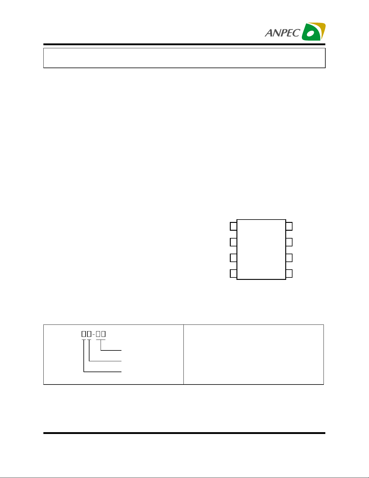
Pin Assignment
XTB
S0
S1
1
2
APV2002
3
8
XT
7
OE
6
VDD
GND
4
SOP − 8
5
QO
Ordering Information
APV2002
Handling Code
Temp. Range
Package Code
ANPEC reserves the right to make changes to improve reliability or manufacturability without notice, and advise
customers to obtain the latest version of relevant information to verify before placing orders.
Copyright ANPEC Electronics Corp.
Rev. A.3 - Nov., 2002
Package Code
K : SOP-8
Y : CHIP FORM
Temp. Range
I : -40 to 85°C
Handling Code
TU : Tube TY : Tray
TR : Tape & Reel W : Wafer
www.anpec.com.tw1
Page 2
APV2002
Pin Description
Pin
1
2
3
4
5
6
7
8
Note1 : Please refer frequency selector
Note2 : High or no connection : enable , Low : disable
Symbol Function
XTB Crystal drive
S0 (Note1) Frequency select pin1
S1 Frequency select pin2
GND Ground
QO Frequency output
VDD Pow er
OE (Note2) Output enable
XT Crystal feedback
Electrical Characteristics
The following specifications apply for VDD = 5V unless otherwise noted.
Symbol Parameter Test Condition
Opera ting condit ion
VDD
Supply Voltage 4.5 5 5.5 V
Ambient Temperature -40 85 °C
APV2002
Min. Typ
.
Max.
Unit
DC characteristics
Freq
IDD Operating Current
V
V
Crystal Frequency 0.5 60
Crystal 50MHz , C
Input Voltage -0.5 VDD+0.5V
IN
Output Voltage -0.5 VDD+0.5V
OUT
= 50pF
L
20
AC characteristics
Duty Waveform Symmetry 40 50 60
Tr
Rise Time 0.5V to 4.5V , C
= 50pF 3 ns
L
Tf Fall Time 4.5V to 0.5V , CL = 50pF 3 ns
Copyright ANPEC Electronics Corp.
Rev. A.3 - Nov., 2002
www.anpec.com.tw2
MHz
mA
%
Page 3

APV2002
Electrical Characteristics (Cont.)
The following specifications apply for VDD = 3.3V unless otherwise noted.
Symbol Parameter Test Condition
Min. Typ
APV2002
.
Max.
Operating condition
VDD
Supply Voltage 3.0 3.3 3.6 V
Ambient Temperatur e -40 85
DC characteristics
Freq
Crystal Frequency 0.5 60
IDD Operating Current Crystal 55MHz , CL = 50pF 20 mA
V
V
Input Voltage -0.5 VDD+0.5V
IN
Output Voltage -0.5 VDD+0.5V
OUT
AC characteristics
Duty Waveform Symmetry 40 50 60
Tr
Rise Time 0.3V to 3.0V , C
= 50pF 3 ns
L
Tf Fall Time 3.0V to 0.3V , CL = 50pF 3 ns
Unit
°C
MHz
%
Copyright ANPEC Electronics Corp.
Rev. A.3 - Nov., 2002
www.anpec.com.tw3
Page 4

APV2002
Pad Layout
1
2
3
4
5 6
11
10
9
8
7
Pad Description
Pad # Symbol Description
1 XTB Crystal drive
2 OE Output enable
3 S0 Frequency select pad1
4 S1 Frequency select pad2
5 GND Ground
6 C/T (Note3) Duty cycle modulation
7 QO Frequency output
8 NC (Note4) Reserve
9 VDD Power
10 OE Output enable
11 XT Crystal feedback
Note3 : C/T-no connection or connect to VDD for above 30Meg XO; connect to GND for below 30Meg XO.
Note4 : NC-no connection
Frequency Selector
S1 S0 QO
X X Default
XO
OX
OO
Note5 : X-no connection , O-connect to GND
Note6 : This function for die use only
Copyright ANPEC Electronics Corp.
Rev. A.3 - Nov., 2002
2
ÒÒÒÒ
4
ÒÒÒÒ
8
ÒÒÒÒ
www.anpec.com.tw4
Page 5

APV2002
Pad Position
Y
2
3
4
(0,0)
Die Size = 716.5um * 821.5um
Pad Size = 86um * 86um
Die Thickness = 250um
Pad # Symbol
1 XTB 260 743
2 OEPAD 78 700
3 S0PAD 78 531
4 S1PAD 78 359
5 G ND 225,321 78,78
6 TCBPAD 468 78
7 QO 638 163
8 NC 638 356
9 VDD 638,638 457,553
10 OEPAD 638 700
11 XT 449 743
Note7 : Substrate should be connected to GND.
Note8 : VDD and GND are double pads.
1
5 6
11
10
9
8
7
x
Pad Center
X(um) Y(um)
Copyright ANPEC Electronics Corp.
Rev. A.3 - Nov., 2002
www.anpec.com.tw5
Page 6

APV2002
Packaging Information
SOP-8 pin ( Reference JEDEC Registration MS-012)
HE
0.015X45
e1 e2
D
A1
A
1
L
0.004max.
Dim
A 1.35 1.75 0.053 0.069
A1 0.10 0.25 0.004 0.010
D 4.80 5.00 0.189 0.197
E 3.80 4.00 0.150 0.157
H 5.80 6.20 0.228 0.244
L 0.40 1.27 0.016 0.050
e1 0.33 0.51 0.013 0.020
e2 1.27BSC 0.50BSC
18
φ
Millimeters Inches
Min. Max. Min. Max.
°
8
°
Copyright ANPEC Electronics Corp.
Rev. A.3 - Nov., 2002
www.anpec.com.tw6
Page 7

APV2002
Physical Specifications
Terminal Material Solder-Plated Copper (Solder Material : 90/10 or 63/37 SnPb)
Lead Solderability Meets EIA Specification RSI86-91, ANSI/J-STD-002 Category 3.
Reflow Condition (IR/Convection or VPR Reflow)
Reference JEDEC Standard J-STD-020A APRIL 1999
Peak temperature
temperature
Pre-heat temperature
°
183 C
Time
Classification Reflow Profiles
Convection or IR/
Convection
Average ramp-up rate(183°C to Peak) 3°C/second max. 10 °C /second max .
Preheat temperature 125 ± 25°C)
Temperature maintained above 183°C
Time within 5°C of actual peak temperature
Peak temperature range
Ramp-down rate
Time 25°C to peak temperature
120 seconds max
60 – 150 seconds
10 –20 seconds 60 seconds
220 +5/-0°C or 235 +5/-0°C 215-219°C or 235 +5/-0°C
6 °C /second max . 10 °C /second max .
6 minutes max.
VPR
Package Reflow Conditions
pkg. thickness
and all bgas
Convection 220 +5/-0 °C Convection 235 +5/- 0 °C
VPR 215-219 °C VPR 235 +5/-0 °C
IR/Convection 220 +5/-0 °C IR/Convection 235 +5/-0 °C
Copyright ANPEC Electronics Corp.
Rev. A.3 - Nov., 2002
2.5mm
≥≥≥≥
pkg. thickness < 2.5mm and
pkg. volume
350 mm³
≥≥≥≥
pkg. thickness < 2.5mm and pkg.
volume < 350mm³
www.anpec.com.tw7
Page 8

APV2002
Reliability test program
T est item Method Description
SOLDERABILITY MIL-STD-883D-2003 245° C,5 SEC
HOLT MIL-STD 883D-1005.7 1000 Hrs Bias @ 125°C
PCT JESD-22-B, A102 168 Hrs, 100% RH, 121°C
TST MIL-STD 883D-1011.9 -65°C ~ 150°C, 200 Cycles
Carrier Tape
W
t
E
F
A
Po
J
P
P1
Ao
C
D
Bo
Ko
D1
T2
B
Application
A B C J T1 T2 W P E
330 ± 1 62 +1.5
SOP- 8
F D D1 Po P1 Ao Bo Ko t
5.5± 1 1.55 +0.1 1.55+ 0.25 4.0 ± 0.1 2.0 ± 0.1 6.4 ± 0.1 5.2± 0. 1 2.1± 0.1 0.3±0.013
Copyright ANPEC Electronics Corp.
Rev. A.3 - Nov., 2002
12.75+
0.15
T1
2 ± 0.5 12.4 ± 0.2 2 ± 0.2 12± 0. 3 8± 0.1 1.75±0.1
www.anpec.com.tw8
Page 9

APV2002
Cover Tape Dimensions
Application Carrier Width Cover Tape Width Devices Per Reel
SOP- 8
Customer Service
Anpec Electronics Corp.
Head Office :
5F, No. 2 Li-Hsin Road, SBIP,
Hsin-Chu, T aiwan, R.O.C.
T el : 886-3-5642000
Fax : 886-3-5642050
Taipei Branch :
7F, No. 137, Lane 235, Pac Chiao Rd.,
Hsin Tien City, Taipei Hsien, Taiwan, R. O. C.
T el : 886-2-89191368
Fax : 886-2-89191369
12 9.3 2500
Copyright ANPEC Electronics Corp.
Rev. A.3 - Nov., 2002
www.anpec.com.tw9
 Loading...