

Page 1
4-Bit Micro-controller With LCD Driver
Features
y Low power and low voltage operation
y Powerful instruction set (150 instructions)
y Memory capacity
Ϋʳ Instruction ROM capacity 4096 x 16 bits
Ϋʳ Index ROM capacity 256 x 8 bits
Ϋʳ Internal RAM capacity 384 or 256 x 4 bits
y Input/Output ports of up to 20 pins
y 8-level subroutine nesting
y Built-in LCD driver, 8 x 42 = 336 segments
y Built-in EL driver, frequency or melody generator
y Built-in Resistance-to-Frequency Converter
y Built-in 2-channel 6/8-bit PWM output
General Description
The APU429 is an embedded high performance
4-bit micro-computer with an on-chip LCD driver. It
contains all the necessary functions in a single chip:
4-bit parallel processing ALU, ROM, RAM, I/O ports,
timer, clock generator, dual clock, RFC, EL-light,
LCD driver, look-up table, watchdog timer and
keyboard scanning. The instruction set includes not
only 4-bit operation and manipulation instructions
but also various conditional branch instructions and
y Built-in key strobe function
(Shared with segment pin)
y Built-in voltage doubler, halver, tripler
quadrupler charge pump circuit
y Two 6-bit programmable timers with
programmable clock source
y Watchdog timer
y 4 external & 3 internal interrupt resources
Ϋʳ External: INT, RFC, IOA/IOC/S port,
keystrobe
Ϋʳ Internal: TM1, TM2, Predivider
y Dual clock operation
y HALT and STOP function
LCD driver data transfer instructions which are
powerful and easy to use.
The HALT function stops any internal operations
other than the oscillator, divider and LCD driver in
order to minimize the power dissipation.
The STOP function stops all the clocks in the chip.
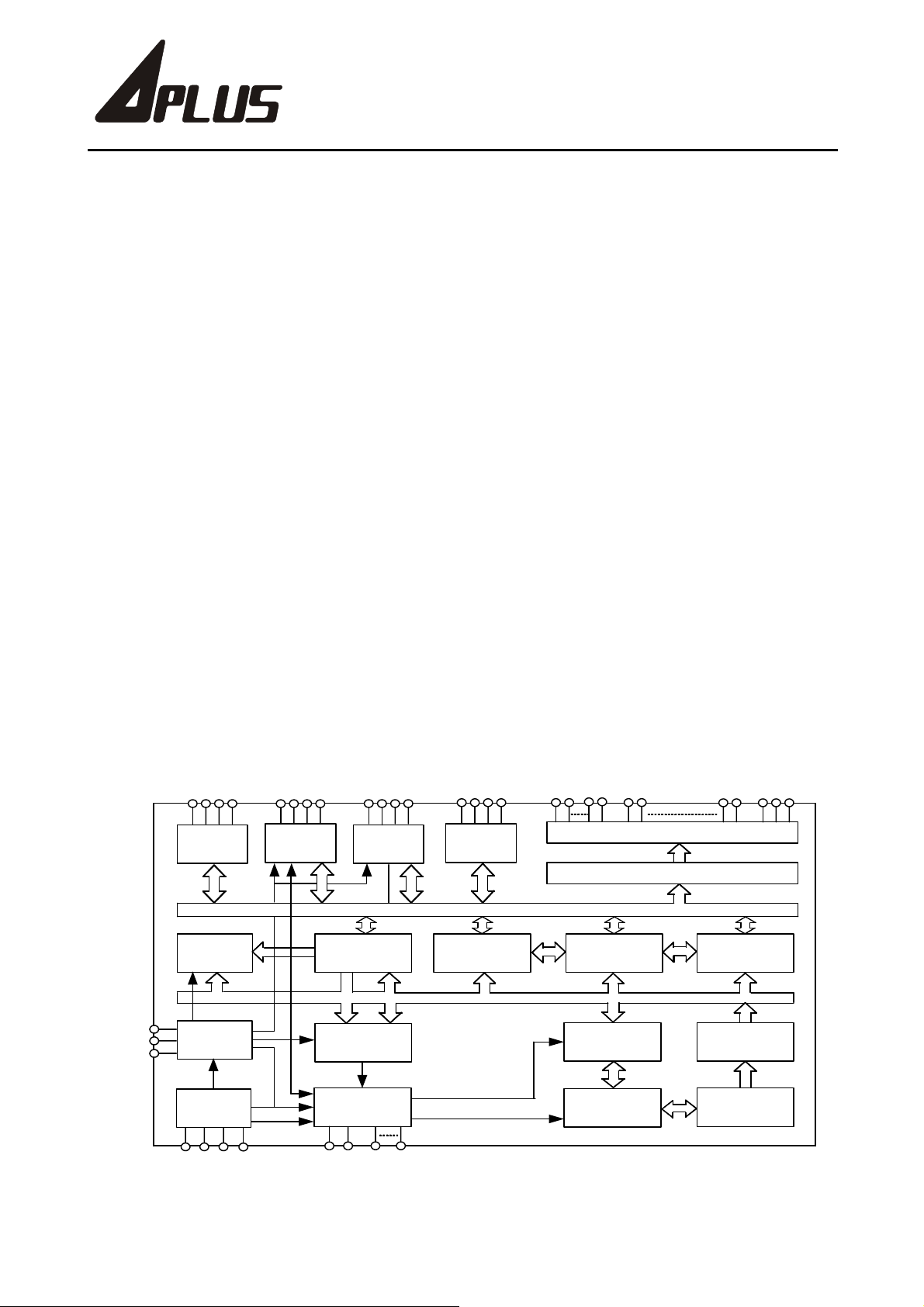
Block Diagram
S E G 3538
IO A P o rt
/R F C
Frequency
Generator
CUP 1
CUP 2
CUP 3
Pre-Divider
W atchdog
Tim er
O s c illa t o r
XTIN
XTOUT
CFIN
CFOUT
S E G 3134
IO B P o rt
/E L , B Z
S E G 3942
IO C P o rt
/K E Y IN
Table R O M
256 x 8
2x6Bits
PresetTimer
Control
Circ u it
S1S4
IN T
RESET
SE G 2730
IO D P o rt
/P W M
4-B itD ata Bus
Index S R AM
256 x 4
COM 18 SEG 1SEG26 VDD14
LC D D river
S egm entP LA
ALU
8-Levels S tack
12-B itProgram
Counter
SRAM
128 x 4
In s tru c tio n
Decoder
MaskROM
4096 x 16
Preliminary
1 Ver.0.0
Page 2
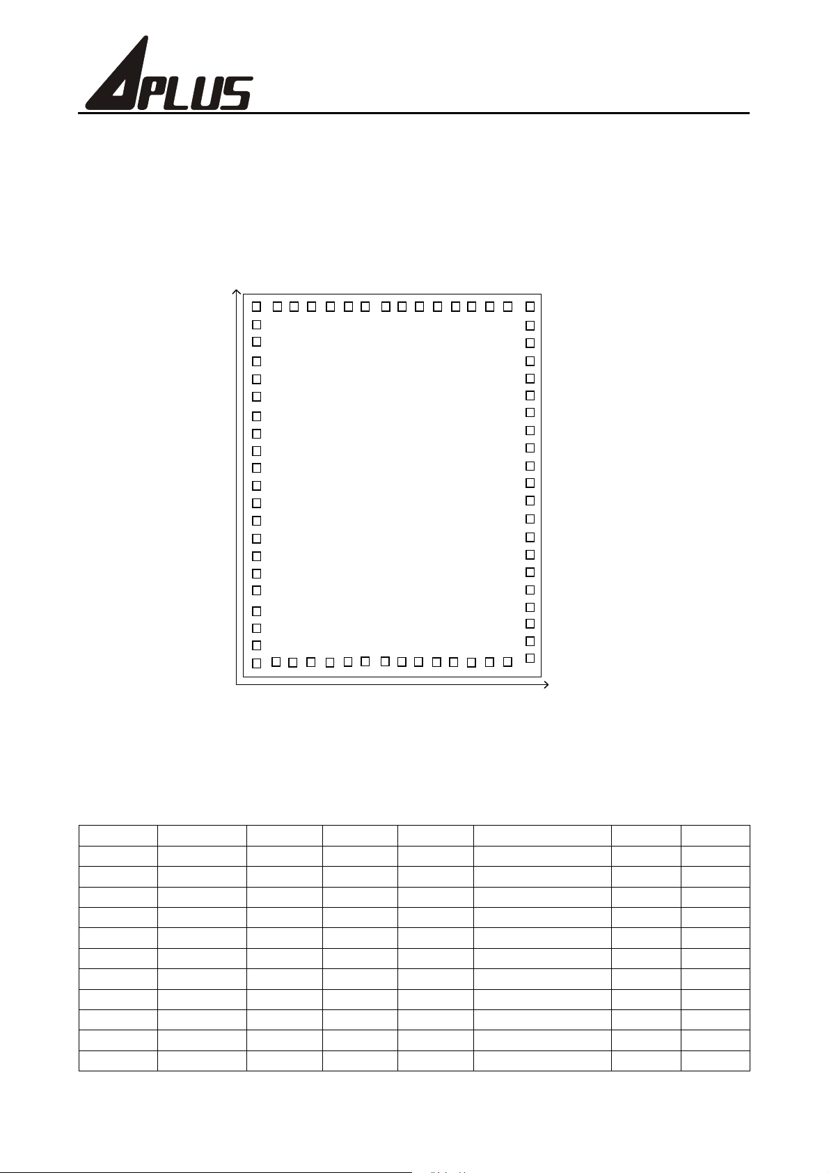
Pad Assignment
APU429
APU429
Chip size : 2620 x 2050 Pm
Pad size : 100 x 100 Pm
Pad window : 90 x 90 Pm
Pad pitch : min. 120 Pm
<
20
10
70
1
60
30
40
50
;
Note: The substrate of die must connect to GND.
Pad Coordinates
Pad No. Pad Name X Y Pad No. Pad Name X Y
1 CFIN 1971.50 2544.50 36 SEG13/KO3 75.25 75.25
2 CFOUT 1785.25 2544.50 37 SEG14/KO4 225.25 75.25
3 XTIN 1665.25 2544.50 38 SEG15/KO5 345.25 75.25
4 XTOUT 1545.25 2544.50 39 SEG16/KO6 465.25 75.25
5 BAK 1425.25 2544.50 40 SEG17/KO7 585.25 75.25
6 TESTA 1305.25 2544.50 41 SEG18/KO8 705.25 75.25
7 RESET 1185.25 2544.50 42 SEG19/KO9 825.25 75.25
8 INT 1065.25 2544.50 43 SEG20/KO10 945.25 75.25
9 S1 945.25 2544.50 44 SEG21/KO11 1065.25 75.25
10 S2 825.25 2544.50 45 SEG22/KO12 1185.25 75.25
11 S3 705.25 2544.50 46 SEG23/KO13 1305.25 75.25
Preliminary
2 Ver.0.0
Page 3
Pad No. Pad Name X Y Pad No. Pad Name X Y
12 S4 585.25 2544.50 47 SEG24/KO14 1425.25 75.25
13 VDD1 465.25 2544.50 48 SEG25/KO15 1545.25 75.25
14 VDD2 345.25 2544.50 49 SEG26/KO16 1665.25 75.25
15 VDD3 225.25 2544.50 50 SEG27/IOD1 1785.25 75.25
16 VDD4 75.25 2544.50 51 SEG28/IOD2 1971.50 75.25
17 CUP1 75.25 2394.50 52 SEH29/IOD3/PWM1 1971.50 225.25
18 CUP2 75.25 2274.50 53 SEH30/IOD4/PWM2 1971.50 345.25
19 CUP3 75.25 2154.50 54 SEG31/IOB1/ELC 1971.50 465.25
20 COM1 75.25 2034.50 55 SEG32/IOB2/ELP 1971.50 585.25
21 COM2 75.25 1914.50 56 SEG33/IOB3/BZB 1971.50 705.25
22 COM3 75.25 1785.25 57 SEG34/IOB4/BZ 1971.50 825.25
23 COM4 75.25 1665.25 58 SEG35/IOA1/CX 1971.50 945.25
24 SEG1 75.25 1545.25 59 SEG36/IOA2/RR 1971.50 1065.25
25 SEG2 75.25 1425.25 60 SEG37/IOA3/RT 1971.50 1185.25
26 SEG3 75.25 1305.25 61 SEG38/IOA4/RH 1971.50 1305.25
27 SEG4 75.25 1185.25 62 SEG39/IOC1/KI1 1971.50 1425.25
28 SEG5 75.25 1065.25 63 SEG40/IOC2/KI2 1971.50 1545.25
29 SEG6 75.25 945.25 64 SEG41/IOC3/KI3 1971.50 1665.25
30 SEG7 75.25 825.25 65 SEG42/IOC4/KI4 1971.50 1785.25
31 SEG8 75.25 705.25 66 COM5 1971.50 1905.25
32 SEG9 75.25 585.25 67 COM6 1971.50 2034.50
33 SEG10 75.25 465.25 68 COM7 1971.50 2154.50
34 SEG11/KO1 75.25 345.25 69 COM8 1971.50 2274.50
35 SEG12/KO2 75.25 225.25 70 GND 1971.50 2394.50
Chip size : 2620 x 2050 Pm
Pad Descriptions
Pad Name I/O Description
BAK
VDD1
VDD2
VDD3
VDD4
RESET I
INT I
TESTA I Test signal input pin.
CUP1
CUP2
CUP3
Preliminary
Positive back-up voltage.
In Li mode, connects a 0.1P capacitance to GND.
LCD drive voltage and positive supply voltage.
While in Ag mode, connects +1.5V to VDD1.
While in Li/ExtV mode, connects +3.0V to VDD2.
Input pin for LSI reset signal.
With Internal pull-down resistor.
Input pin for external INT request signal.
Falling edge or rising edge triggered by mask option.
Internal pull-down or pull-up resistor or floatting to be selected by mask option.
TESTA I Test signal input pin, internal pull-down resistor.
Switching pins for supplying the LCD driving voltage to the VDD1, 2, 3, 4 pins.
Connects the CUP1, CUP2 and CUP3 pins with a nonpolarized electronic
O
capacitor if 1/2, 1/3 or 1/4 bias mode has been selected. In the STATIC mode,
these pins should be open.
3 Ver.0.0
Page 4
Pad Name I/O Description
Time based counter frequency (Clock specified. LCD alternating frequency.
Alarm signal frequency.) or system clock oscillation.
XTIN
XTOUT
CFIN
CFOUT
COM1~8 O Output pins for supplying voltage to drive the common pins of the LCD panel.
SEG1~10 O Output pins for LCD panel segment.
SEG11~26/KO1~16 O
SEG27~42 O Output pins for LCD panel segment.
IOA1~4 I/O
IOB1~4
IOC1~4 I/O
IOD1~4 I/O
S1~4 I
KI1~4 I Key scan input, this port shares pins with IOC1~4 and is set by mask option.
CC
RFC RR
RT
RH
EL ELC
ELP
ALM BZB
BZ
PWM1, 2 O 6/8-Bit PWM output; set by mask option.
GND Negative supply voltage.
I
32KHz crystal oscillator.
O
Oscillation stops at the execution of STOP instruction.
System clock oscillation.
Connected with ceramic resonator.
I
Connected with RC oscillation circuit.
O
Oscillation stops at the execution of STOP or SLOW instruction.
Output pins for LCD panel segment.
Key strobe function, share pins as key scan output.
Input/Output port A, can use software to define the internal pull-low resistor
and chattering clock in order to reduce input bounce and generate an
interrupt.
This port shares pins with SEG35~38 and is set by mask option.
This port also shares pins with CC, RR, RT and RH, and is set by mask option.
Input/Output port B.
IOB port shares pins with SEG31~34, and is set by mask option.
I/O
This port also shares pins with ELC, ELP, BZB and BZ, and is set by mask
option.
Input/Output port C, can use software to define internal pull-low/low-level hold
resistor and chattering clock in order to reduce input bounce and generate an
interrupt or keyboard scanning function with ELC, ELP, BZB and BZ, and is
set by mask option.
Input/Output port D.
This port shares pins with SEG27~30 and is set by mask option.
IOD3, 4 shares pins with PWM1, 2 and is set by mask option.
Input ports by mask option to internal pull-low/low-level hold resistor and
chattering clock in order to reduce input bounce and generate an interrupt or
HALT or STOP release.
I
1 input pin and 3 output pins for RFC application.
O
This port shares pins with SEG35~38 and is set by mask option.
O
This port shares pins with IOA1~4 and is set by mask option.
O
OOOutput port for EL-light.
This port shares pins with SEG31, 32 and is set by mask option.
This port shares pins with IOB1, 2 and is set by mask option.
O Output port for alarm, frequency or melody generator.
This port shares pins with IOB3, 4 and is set by mask option.
Preliminary
4 Ver.0.0
Page 5
Absolute Maximum Rating Ta = 0 to 70к GND=0V
Name Symbol Rating Unit
Maximum Supply Voltage
V
V
V
V
Maximum Input Voltage V
V
V
Maximum Operating Temperature t
Maximum Storage Temperature t
DD1
DD2
DD3
DD4
IN
OUT1
OUT2
OPG
STG
-0.3 ~ +5.5 V
-0.3 ~ +5.5 V
-0.3 ~ +8.5 V
-0.3 ~ +8.5 V
-0.3 to V
-0.3 to V
-0.3 to V
+0.3 V
DD1/2
+0.3 VMaximum Output Voltage
DD1/2
+0.3 V
DD3
0 to +70
-25 to +125
к
к
Allowable operating conditions Ta = 0 to 70к GND=0V
Name Symbol Condition Min. Max. Unit
Supply Voltage
Oscillator Start-up Voltage V
Oscillator Sustain Voltage V
Supply Voltage V
Supply Voltage V
Input sHs Voltage
Input sLs Voltage
Input sHs Voltage
Input sLs Voltage
Input sHs Voltage
Input sLs Voltage
Input sHs Voltage
Input sLs Voltage
Input sHs Voltage
Input sLs Voltage
Input sHs Voltage
Input sLs Voltage
Operating Freq.
V
DD1
V
DD2
V
DD3
V
DD4
DDB
DDB
DD1
DD2
V
V
V
V
V
V
V
V
V
V
V
V
f
OPG1
f
OPG2
f
OPG3
Crystal Mode 1.3 V
Crystal Mode 1.2 V
Ag Mode 1.2 1.65 V
EXT-V, Li Mode 2.4 5.25 V
Ag Battery Mode V
IH1
IL1
Li Battery Mode
IH2
IL2
OSCIN at Ag Battery Mode
IH3
IL3
OSCIN at Li Battery Mode
IH4
IL4
CFIN at Li Battery or EXT-V Mode
IH5
IL5
IH6
RC Mode
IL6
Crystal Mode 32 3580 kHz
External RC Mode 32 1000 kHz
CF Mode 1000 3580 kHz
1.2 5.25 V
2.4 5.25 V
2.4 8.0 V
2.4 8.0 V
DD1-0.7
V
DD1+0.7
-0.7 0.7 V
V
DD2-0.7
V
DD2+0.7
-0.7 0.7 V
0.8V
DD1
00.2V
0.8V
DD2
00.2V
0.8V
DD2
00.2V
0.8V
DDO
00.2V
V
DD1
DD1
V
DD2
DD2
V
DD2
DD2
V
DDO
DDO
V
V
V
V
V
V
V
V
V
V
Preliminary
5 Ver.0.0
Page 6
Electrical Characteristics
Input resistance
Name Symbol Condition Min. Typ. Max. Unit
sLs-Level Hold tR(IOC)
IOC/IOA Pull-Down t
INT Pull-Up t
R
INT Pull-Down t
RES Pull-Down t
R
R
R
R
R
R
R
R
R
R
R
R
R
R
R
R
R
R
IIH1
IIH2
IIH3
MSD1
MSD2
MSD3
INTU1
INTU2
INTU3
INTD1
INTD2
INTD3
RES1
RES2
RES3
VI=0.2V
VI=0.2V
VI=0.2V
VI=V
VI=V
VI=V
VI=V
VI=V
VI=V
, #1 10 40 100
DD1
, #2 10 40 100
DD2
, #3 5 20 50
DD2
, #1 200 500 1000
DD1
, #2 200 500 1000
DD2
, #3 100 250 500
DD3
, #1 200 500 1000
DD1
, #2 200 500 1000
DD2
, #3 100 250 500
DD3
VI=GND, #1 200 500 1000
VI=GND, #2 200 500 1000
VI=GND, #3 100 250 500
VI=GND or V
VI=GND or V
VI=GND or V
, #1 5 20 50
DD1
, #2 5 20 50
DD2
, #3 5 20 50
DD2
k:
k:
k:
k:
k:
k:
k:
k:
k:
k:
k:
k:
k:
k:
k:
Note: #1: V
= 1.2V ( Ag ), #2: V
DD1
DC output characteristics
Name Symbol Condition For Min. Typ. Max. Unit
Output sHs Voltage
Output sLs Voltage
Output sHs Voltage
Output sLs Voltage
Note: #1: V
= 1.2V ( Ag ), #2: V
DD1
V
OH1a
V
OH2 a
V
OH3 a
V
OL1 a
V
OL2 a
V
OL3 a
V
OH1c
V
OH2cIOH
V
OH3cIOH
V
OL1c
V
OL2cIOL
V
OL3CIOL
= 2.4V ( Li ), #3: V
DD2
IOH=-10PA, #1
IOH=-50PA, #2
IOH=-200PA, #3
IOL=20PA, #1
IOL=100PA, #2
IOL=400PA, #3
IOH=-200PA, #1
= 4V (Ext-V).
DD2
SEG1~26
0.8 0.9 1.0 V
1.5 1.8 2.1 V
2.5 3 3.5 V
0.2 0.3 0.4 V
0.3 0.6 0.9 V
0.5 1 1.5 V
0.8 0.9 1.0 V
=-1mA, #2 1.5 1.8 2.1 V
=-3mA, #3 2.5 3 3.5 V
IOL=400PA, #1
SEG27~42
IOA, B, C, D
0.2 0.3 0.4 V
=2mA, #2 0.3 0.6 0.9 V
=6mA, #3
= 2.4V ( Li ), #3: V
DD2
= 4V (Ext-V).
DD2
0.5 1 1.5 V
Preliminary
6 Ver.0.0
Page 7

Segment driver output characteristics
Name Symbol Condition For Min. Typ. Max. Unit
Static display mode
Output sHs Voltage
Output sLs Voltage
Output sHs Voltage
Output sLs Voltage
V
V
V
V
V
V
V
V
V
V
V
V
OH1d
OH2d
OH3d
OL1d
OL2d
OL3d
OH1e
OH2e
OH3e
OL1e
OL2e
OL3e
IOH=-1PA, #1
I
IOH=-1PA, #3
IOL=1PA, #1
IOL=1PA, #2
IOL=1PA, #1
IOH=-10PA, #1
IOH=-10PA, #2
I
IOL=10PA, #1
IOL=10PA, #2
IOL=10PA, #3
1/2 bias display mode
Output sHs Voltage
Output sLs Voltage
Output sHs Voltage
Output sMs Voltage
Output sLs Voltage
V
V
V
V
V
V
V
V
V
V
OH12f
OH3f
OL12f
OL3f
OH12g
OH3g
OM12g
OM3g
OL12g
OL3g
IOH=-1PA, #1, #2
IOH=-1PA, #3
IOL=1PA, #1, #2
IOL=1PA, #3
IOH=-10PA, #1, #2
IOH=-10PA, #3
I
I
IOL=10PA, #1, #2
IOL=10PA, #3
1/3 bias display mode
Output sHs Voltage
Output sM1s Voltage
Output sM2s Voltage
Output sLs Voltage
Output sHs Voltage
Output sM1s Voltage
Output sM2s Voltage
Output sLs Voltage
Note: #1: V
= 1.2V ( Ag ), #2: V
DD1
V
V
V
V
V
V
V
V
V
V
V
V
V
V
V
V
OH12i
OH3i
OM12i
OM13i
OM22i
OM23i
OL12i
OL3i
OH12j
OH3j
OM12j
OM13j
OM22j
OM23j
OL12j
OL3j
IOH=-1PA, #1, #2
IOH=-1PA, #3
I
I
I
I
IOL=1PA, #1, #2
IOL=1PA, #3
IOH=-10PA, #1, #2
IOH=-10PA, #3
I
I
I
I
IOL=10PA, #1, #2
I
= 2.4V ( Li ), #3: V
DD2
=-1PA, #2
OH
=-10PA, #3
OH
=r10PA, #1, #2
OI/H
=r10PA, #3
OI/H
=r10PA, #1, #2
OI/H
=r10PA, #3
OI/H
=r10PA, #1, #2
OI/H
=r10PA, #13
OI/H
=r10PA, #1, #2
OI/H
=r10PA, #3
OI/H
=r10PA, #1, #2
OI/H
=r10PA, #3
OI/H
=10PA, #3
OL
SEG-n
COM-n
SEG-n
COM-n
SEG-n
COM-n
= 4V (Ext-V).
DD2
1.0 V
2.2 V
3.8 V
0.2 V
0.2 V
0.2 V
1.0 V
2.2 V
3.8 V
0.2 V
0.2 V
0.2 V
2.2 V
3.8 V
0.2 V
0.2 V
2.2 V
3.8 V
1.0 1.4 V
1.8 2.2 V
0.2 V
0.2 V
3.4 V
5.8 V
1.0 1.4 V
1.8 2.2 V
2.2 2.6 V
3.8 4.2 V
0.2 V
0.2 V
3.4 V
5.8 V
1.0 1.4 V
1.8 2.2 V
2.2 2.6 V
3.8 4.2 V
0.2 V
0.2 V
Preliminary
7 Ver.0.0
Page 8

Functional Description
SRAM
The 256 x 4 bits index SRAM and 128 x 4 bits data SRAM are 2 separate regions.
Index ROM
The 256 x 8 bits index ROM can be used as a 4-bit mode or an 8-bit mode.
I/O ports
The IOA port can be selected by software separately as input or output, and with/without internal pull-low and
different chattering clocks in order for HALT release/ interrupt trigger to reduce the bounce of key_scan:
PH6: 512Hz PH8:128Hz PH10: 32Hz
The pull-low of the IOA will be masked off for those pins defined as output pins.
The IOA port can be used as a pseudo serial output port.
The IOB port can be selected by software separately as input or output.
The IOC port can be selected by software separately as input or output, and with/without internal pull-low and
different chattering clocks in order for HALT release/ interrupt trigger to reduce the bounce of key_scan.
The IOD port can be selected by software separately as input or output.
The IOD port can be used as a pseudo serial output port.
The initial state of all I/O ports is standard input state and IOA, C have pull-low device.
Before setting some pins from input to output, you can execute the output function to ensure their output value.
The S ports are input pins that contain pull-low. The L_L_H resistor can be selected by mask option and
different chattering clocks in the same manner as the IOA, C ports.
Resistor to frequency converter
We use an RC oscillation circuit and a 16-bit counter to calculate the relative resistance of temperature and
humidity sensor. The diagram is shown below:
RTP
RT
RHM
RH
Rref
RR
CX
CX
ELP
ENX
EHM
FIN
ERR
ENX
FIN
Timer & R/F
Controller
Freq.
Freq.
CL LD
CL LD
16-Bit Counter
4-Bit Data Bus
TMS
PH9
MRF
There are two types of methodology for measuring the input frequency: first, set FIN (i.e. CX) as the clock
input, using timer 2 as interval control or using software to directly control the interval. Second, if the FIN (CX)
frequency is too low, either because of a poor resolution for a fixed interval or a longer interval for better
Preliminary
8 Ver.0.0
Page 9

resolution but with a longer read-out rate (for example: 10 seconds per read-out), you can switch the measure
mode in order to set FIN (CX) as interval control (it will enable the counter from first FIN rising edge to the next
rising edge, then will generate an interrupt) and use FREQ (internal frequency generator output) as clock
input, hence you can count the interval of CX.
To measure the resistor value of the temperature and humidity sensor, we must first measure the frequency
of Rref, then the frequency of sensor.
Fref= K/Rref CX and
Fsensor= K/Rsensor CX, hence
Rsensor= Rref * Freq/Fsensor.
Where K is a coefficient for RC-oscillation and will be a constant in a short time period.
Keyboard scanning function
SEG11~26 shares the keyboard scanning output, the output of the keyboard scanning is a P open-drain to
VDDO (positive power supply) and all other SEGs and COMs are in Hi-z state during this period. This will
minimize the effect of the LCD output.
The segment 11-26 also could be used as keyscan output and LCD still could be displayed with only slightly
affected.
SPK 00b5 b4 b3 b2 b1 b0.
b5: 1 will disable key-scan output.
b4: 1 will set all keyscan output as high, if b5=0.
b3~b0: will set the corresponding segment output as 1, if b5=0 and b4=0.
During power on, LCD off, STOP condition. All the common & segment output will be the chips supply power.
EL-light
Set the ELC and ELP clock and duty cycle by ELC X instruction, then turn on and off the ELC and ELP output
by SF X and RF X instruction. With external transistor, diode, inductor and resistor, we can pump the Elpanel
to AC 100~250V.
L1
D1
R1
ELP
R2
ELC
LIT
ELP
Q1
EL-plane
Q2
ELC
While the light is turned on, the ELC will turn on before the ELP, but when the light is turned off, the ELP and
ELC will turn off after the next falling edge of the ELC to make sure no voltage is left on the EL- panel.
Preliminary
9 Ver.0.0
Page 10

Timer
The 6-bit programmable timer can select PH3/PH9/PH15/FREQ (timer 2 can also select PH5/PH7/PH11/
PH13 by TM2X instruction) as the clock source. When it underflows, the HALT release signal is generated.
Predivider
The predivider is a 15-stage counter that uses PH0 as the clock source. The output of T-F/F is changed when
the input signal is changed from H to L. PH11~15 are reset to L when PLC 100H instruction is executed, or
power-on or external reset is used. When PH14 is changed from H to L, the HALT release signal is generated.
Alarm/frequency/melody
There is an 8-bit programmable counter and an 8-bit envelope control for alarm, frequency or melody output
from BZ/BZB.
The frequency counter can use software to select 1/2 duty, 1/3 duty or 1/4 duty drive mode.
Freq.
1/2 Duty Frequency
1/3 Duty Frequency
1/4 Duty Frequency
INT function
The INT pin can be selected by mask option as pull-high/pull-low or none, and rising edge/falling edge trigger.
Watchdog timer
The watchdog timer automatically generates a device reset when it overflows. The interval of overflow is
8/64/512 x PH10 (set by mask option). You can use software to enable and disable this function. The
watchdog enable flag will be disabled by power-on reset or reset-pin reset condition, but cannot be disabled
by watchdog reset itself.
HALT function
The HALT instruction will disable all clocks except the predivider, timer, frequency counter, PWM, EL-light
generator and chattering clock to minimize the operating current.
STOP function
The STOP instruction will disable all clocks to minimize the standby current, so only two external factors (INT,
IOA/IOC/S port, keyscan) can release the STOP condition.
Instruction Table (Total 150 instructions)
Instruction Machine Code Function Flag/Remark
NOP 0000 0000 0000 0000 No Operation
LCT Lz, Ry 0000 001Z ZZZZ YYYY
LCB Lz, Ry 0000 010Z ZZZZ YYYY
LCP Lz, Ry 0000 011Z ZZZZ YYYY
LCD Lz, @HL 0000 100Z ZZZZ 0000
LCT Lz, @HL 0000 100Z ZZZZ Z-01 Lz {7SEG @HL
Lz Чʳ { 7SEG Чʳ Ry}
Lz Чʳ { 7SEG Чʳ Ry}
Lz Ч Ry , AC
Lz Ч T@HL
Preliminary
10 Ver.0.0
Page 11

Instruction Machine Code Function Flag/Remark
LCB Lz, @HL 0000 100Z ZZZZ Z-10 Lz {7SEG @HL
LCP Lz, @HL 0000 100Z ZZZZ Z-11 Lz @HL, AC
OPA Rx 0000 1010 0XXX XXXX
OPAS Rx, D 0000 1011 DXXX XXXX
OPB Rx 0000 1100 0XXX XXXX
OPC Rx 0000 1101 0XXX XXXX
OPD Rx 0000 1110 0XXX XXXX
OPDS Rx 0000 1111 DXXX XXXX
Port(A) Чʳ Rx
A1, 2, 3, 4 Чʳ Rx0, Rx1, D, Pulse
Port(B) Чʳ Rx
Port(C) Чʳ Rx
Port(D) Чʳ Rx
D1, 2, 3, 4 Чʳ Rx0, Rx1, D, Pulse
FREQ Чʳ Rx, AC
DD=00: 1/4 Duty
FRQ Rx, D
0001 00DD 0XXX XXXX
DD=01: 1/3 Duty
DD=10: 1/2 Duty
DD=11: 1/1 Duty
FRQ D,@HL 0001 01DD 0000 0000
FRQX D,X 0001 10DD XXXX XXXX
MVL Rx 0001 1100 0XXX XXXX
MVH Rx 0001 1101 0XXX XXXX
MPW1 Rx 0001 1110 0XXX XXXX
MPW2 Rx 0001 1111 0XXX XXXX
ADC Rx 0010 0000 0XXX XXXX
ADC @HL 0010 0000 1000 0000
ADC* Rx 0010 0001 0XXX XXXX
ADC* @HL 0010 0001 1000 0000
SBC Rx 0010 0010 0XXX XXXX
SBC @HL 0010 0010 1000 0000
SBC* Rx 0010 0011 0XXX XXXX
SBC* @HL 0010 0011 1000 0000
ADD Rx 0010 0100 0XXX XXXX
ADD @HL 0010 0100 1000 0000
ADD* Rx 0010 0101 0XXX XXXX
ADD* @HL 0010 0101 1000 0000
SUB Rx 0010 0110 0XXX XXXX
SUB @HL 0010 0110 1000 0000
SUB* Rx 0010 0111 0XXX XXXX
SUB* @HL 0010 0111 1000 0000
ADN Rx 0010 1000 0XXX XXXX
ADN @HL 0010 1000 1000 0000
ADN* Rx 0010 1001 0XXX XXXX
ADN* @HL 0010 1001 1000 0000
AND Rx 0010 1010 0XXX XXXX
AND @HL 0010 1010 1000 0000
FREQ
FREQ
L
H
PWM1
PWM2
AC Ч Rx+AC+CF
AC Ч @HL+AC+CF
AC, Rx Ч Rx+AC+CF
AC, @HL Ч @HL+AC+CF
AC Ч Rx+ACB+CF
AC Ч @HL+ACB+CF
AC, Rx Ч Rx+ACB+CF
AC, @HL Ч @HL+ACB+CF
AC Ч Rx+AC
AC Ч @HL+AC
AC,Rx Ч Rx+AC
AC, @HL Ч @HL+AC
AC Ч Rx+ACB+1
AC Ч @HL+ACB+1
AC, Rx Ч Rx+ACB+1
AC,@HL Ч @HL+ACB+1
AC Ч Rx+AC
AC Ч @HL+AC
AC, Rx Ч Rx+AC
AC,@HL Ч @HL+AC
AC Ч Rx AND AC
AC Ч @HL AND AC
Ч T@HL
Ч X
Ч Rx
Ч Rx
Ч Rx , AC
Ч Rx , AC
CF
CF
CF
CF
CF
CF
CF
CF
CF
CF
CF
CF
CF
CF
CF
CF
Preliminary
11 Ver.0.0
Page 12

Instruction Machine Code Function Flag/Remark
AND* Rx 0010 1011 0XXX XXXX
AND* @HL 0010 1011 1000 0000
EOR Rx 0010 1100 0XXX XXXX
EOR @HL 0010 1100 1000 0000
EOR* Rx 0010 1101 0XXX XXXX
EOR* @HL 0010 1101 1000 0000
OR Rx 0010 1110 0XXX XXXX
OR @HL 0010 1110 1000 0000
OR* Rx 0010 1111 0XXX XXXX
OR* @HL 0010 1111 1000 0000
ADCI Ry,D 0011 0000 DDDD YYYY
ADCI* Ry,D 0011 0001 DDDD YYYY
SBCI Ry,D 0011 0010 DDDD YYYY
SBCI* Ry,D 0011 0011 DDDD YYYY
ADDI Ry,D 0011 0100 DDDD YYYY
ADDI* Ry,D 0011 0101 DDDD YYYY
SUBI Ry,D 0011 0110 DDDD YYYY
SUBI* Ry,D 0011 0111 DDDD YYYY
ADNI Ry,D 0011 1000 DDDD YYYY
ADNI* Ry,D 0011 1001 DDDD YYYY
ANDI Ry,D 0011 1010 DDDD YYYY
ANDI* Ry,D 0011 1011 DDDD YYYY
EORI Ry,D 0011 1100 DDDD YYYY
EORI* Ry,D 0011 1101 DDDD YYYY
ORI Ry,D 0011 1110 DDDD YYYY
ORI* Ry,D 0011 1111 DDDD YYYY
INC* Rx 0100 0000 0XXX XXXX
INC* @HL 0100 0000 1000 0000
DEC* Rx 0100 0001 0XXX XXXX
DEC* @HL 0100 0001 1000 0000
IPA Rx 0100 0010 0XXX XXXX
IPB Rx 0100 0100 0XXX XXXX
IPS Rx 0100 0110 0XXX XXXX
IPC Rx 0100 0111 0XXX XXXX
IPD Rx 0100 1000 0XXX XXXX
MAF Rx 0100 1010 0XXX XXXX
AC, Rx Ч Rx AND AC
AC,@HL Ч @HL AND AC
AC Ч Rx EOR AC
AC Ч @HL EOR AC
AC, Rx Ч Rx EOR AC
AC,@HL Ч @HL EOR AC
AC Ч Rx OR AC
AC Ч @HL OR AC
AC, Rx Ч Rx OR AC
AC,@HL Ч @HL OR AC
AC Ч Ry+D+CF CF
AC, Ry Ч Ry+D+CF
AC Ч Ry+DB+CF
AC, Ry Ч Ry+DB+CF
AC Ч Ry+D
AC, Ry Ч Ry+D
AC Ч Ry+DB+1
AC, Ry Ч Ry+DB+1
AC Ч Ry+D
AC, Ry Ч Ry+D
AC Ч Ry AND D
AC, Ry Ч Ry AND D
AC Ч Ry EOR D
AC, Ry Ч Ry EOR D
AC Ч Ry OR D
AC, Ry Ч Ry OR D
AC, Rx Ч Rx+1
AC, @HL Ч @HL+1
AC, Rx Ч Rx-1
AC, @HL Ч @HL-1
AC, Rx Ч Port(A)
AC, Rx Ч Port(B)
AC, Rx Ч Port(S)
AC, Rx Ч Port(C)
AC, Rx Ч Port(D)
AC,Rx Ч STS1
CF
CF
CF
CF
CF
CF
CF
CF
CF
CF
CF
B3: CF
B2: ZERO
B1: (No use)
B0: (No use)
Preliminary
12 Ver.0.0
Page 13

Instruction Machine Code Function Flag/Remark
B3: (No use)
MSB Rx 0100 1011 0XXX XXXX
MSC Rx
MCX Rx
MSD Rx
SR0 Rx 0101 0000 0XXX XXXX
SR1 Rx 0101 0001 0XXX XXXX
SL0 Rx 0101 0010 0XXX XXXX
SL1 Rx 0101 0011 0XXX XXXX
DAA 0101 0100 0000 0000
DAA* Rx 0101 0101 0XXX XXXX
DAA* @HL 0101 0101 1000 0000
DAS 0101 0110 0000 0000
DAS* Rx 0101 0111 0XXX XXXX
DAS* @HL 0101 0111 1000 0000
LDS Rx,D 0101 1DDD DXXX XXXX
LDH Rx,@HL 0110 0000 0XXX XXXX
LDH* Rx,@HL 0110 0001 0XXX XXXX
LDL Rx,@HL 0110 0010 0XXX XXXX
LDL* Rx,@HL 0110 0011 0XXX XXXX
MRF1 Rx 0110 0100 0XXX XXXX
MRF2 Rx 0110 0101 0XXX XXXX
MRF3 Rx 0110 0110 0XXX XXXX
MRF4 Rx 0110 0111 0XXX XXXX
STA Rx 0110 1000 0XXX XXXX
STA @HL 0110 1000 1000 0000
0100 1100 0XXX XXXX
0100 1101 0XXX XXXX
0100 1110 0XXX XXXX
AC,Rx Ч STS2
AC,Rx Ч STS3
AC,Rx Ч STS3X
AC,Rx Ч STS4
ACn, Rxn Ч Rx(n+1)
AC3, Rx3 Ч 0
ACn, Rxn Ч Rx(n+1)
AC3, Rx3 Ч 1
ACn, Rxn Ч Rx(n-1)
AC0, Rx0 Ч 0
Can, Rxn Ч Rx(n-1)
AC0, Rx0 Ч 1
AC Ч BCD(AC)
AC, Rx Ч BCD(AC)
AC, @HL Ч BCD(AC)
AC Ч BCD(AC)
AC, Rx Ч BCD(AC)
AC, @HL Ч BCD(AC)
AC, Rx Ч D
AC, Rx Ч H(T@HL)
AC, Rx Ч H(T@HL)
HL Ч HL + 1
AC, Rx Ч L(T@HL)
AC, Rx Ч L(T@HL)
HL Ч @HL + 1
AC,Rx Ч RFC3-0
AC,Rx Ч RFC7-4
AC,Rx Ч RFC11-8
AC,Rx Ч RFC15-12
Rx Ч AC
@HL Ч AC
B2: SCF2(HRx)
B1: SCF1(CPT)
B0: BCF
B3: SCF7(PDV)
B2: PH15
B1: SCF5(TMR1)
B0: SCF4(INT)
B3: SCF9(RFC)
B2: SCF0(APT)
B1: SCF6(TMR2)
B0: (No use)
B3: (No use)
B2: RFOVF
B1: WDF
B0: CSF
CF
CF
CF
CF
CF
CF
Preliminary
13 Ver.0.0
Page 14

Instruction Machine Code Function Flag/Remark
LDA Rx 0110 1100 0XXX XXXX
LDA @HL 0100 1100 1000 0000
MRA Rx 0110 1101 0XXX XXXX
MRW @HL,Rx 0110 1110 0XXX XXXX
MWR Rx,@HL 0110 1111 0XXX XXXX
MRW Ry,Rx 0111 0YYY YXXX XXXX
MWR Rx,Ry 0111 1YYY YXXX XXXX
JB0 X 1000 0XXX XXXX XXXX
JB1 X 1000 1XXX XXXX XXXX
JB2 X 1001 0XXX XXXX XXXX
JB3 X 1001 1XXX XXXX XXXX
JNZ X 1010 0XXX XXXX XXXX
JNC X 1010 1XXX XXXX XXXX
JZ X 1011 0XXX XXXX XXXX
JC X 1011 1XXX XXXX XXXX
CALL X 1100 0XXX XXXX XXXX
JMP X 1101 0XXX XXXX XXXX
RTS 1101 1000 0000 0000
SCC X 1101 1001 0XXX XXXX
SCA X
(SMS)
SPA X 1101 1100 000X XXXX
SPB X 1101 1101 0000 XXXX X3~0: Set D4~1 I/O
SPC X
SPD X 1101 1111 0000 XXXX X3-0: Set D4~1 I/O
TMS Rx 1110 0000 0XXX XXXX
TMS @HL 1110 0001 0000 0000
1101 1010 00XX XXXX
1101 1110 000X XXXX
AC Ч Rx
AC Ч @HL
CF Ч Rx3
AC,@HL Ч Rx
AC,Rx Ч @HL
AC,Ry Ч Rx
AC,RxҏЧҏRy
PC Ч X
PC Ч X
PC Ч X
PC Ч X
PC Ч X
PC Ч X
PC Ч X
PC Ч X
STACK Ч PC+1
PC Ч X
PC Ч X
PC Ч STACK
X6 = 1: Cfq = BCLK
X6 = 0: Cfq = PH0
X5 = 1: Cpw = BCLK
X5 = 1: Cpw = PH0
X4, 3 = 1X: Set P(A)
X4, 3 = 01: Set P(S)
X4, 3 = 00 Set P (C)
X2,1,0=001: Cch = PH10
X2,1,0=010: Cch = PH8
X2,1,0=1XX: Cch = PH6
X0~3: S1~4 Enable (SEF0~3)
X5: A1-4 Enable (SEF5)
X4: C1-4 Enable (SEF4)
X4: Set A4~1 Pull-Low
X3~0: Set A4~1 I/O
X4: Set C4-1 Pull-Low/
Low-Level-Hold
X3~0: Set C4-1 I/O
Timer1 Ч Rx, AC
Timer1 Ч T@HL
if AC0 = 1
if AC1 = 1
if AC2 = 1
if AC3 = 1
if AC z 0
if CF = 0
if AC0 = 0
if CF = 1
CALL Return
Preliminary
14 Ver.0.0
Page 15

Instruction Machine Code Function Flag/Remark
X7,6=11: Ctm=FREQ
X7,6=10: Ctm=PH15
TMSX
SPK Rx 1110 0011 00XX XXXX
TM2 Rx 1110 0100 0XXX XXXX
TM2 @HL 1110 0101 0000 0000
TM2X X 1110 011X XXXX XXXX
SHE X 1110 1000 0XXX XXX0
SIE* X 1110 1001 0XXX XXXX
PLC X 1110 101X 0XXX XXXX
SRF X 1110 1100 00XX XXXX
SRE X 1110 1101 X0XX 0000
FAST 1110 1110 0000 0000 SCLK: High Speed Clock
SLOW 1110 1111 0000 0000 SCLK: Low Speed Clock
1110 0010 XXXX XXXX
X7,6=01: Ctm=PH3
X7,6=00: Ctm=PH9
X5~0: Set Timer1 Value
X5 = 1: Set all Hi-Z
X4 = 1: Set all = 1
X3 = 0: Set n of 16
Timer2ҏЧҏRx, AC
Timer2ҏЧҏT@HL
X8,7,6=111 : Ctm=PH13
X8,7,6=110 : Ctm=PH11
X8,7,6=101 : Ctm=PH7
X8,7,6=000 : Ctm=PH5
X8,7,6=011 : Ctm=FREQ
X8,7,6=010 : Ctm=PH15
X8,7,6=001 : Ctm=PH3
X8,7,6=000 : Ctm=PH9
X5~0: Set Timer2 Value
X6: Enable HEF6(RFC)
X4: Enable HEF4(TMR2)
X3: Enable HEF3(PDV)
X2: Enable HEF2(INT)
X1: Enable HEF1(TMR1)
X6: Enable IEF6(RFC)
X5: Enable IEF5(KEY_S)
X4: Enable IEF4(TMR2)
X3: Enable IEF3(PDV)
X2: Enable IEF2(INT)
X1: Enable IEF1(TMR1)
X0: Enable IEF0(A,CPT)
X8: Reset PH15~11
X6, 4~0: Reset HRF6, 4~0
X5: Enable Cx Control
X4: Enable Timer2 Control
X3: Enable Counter
X2: Enable RH Output
X1: Enable RT Output
X0: Enable RR Output
X7: Enable SRF7
X6: Enable SRF6
X5: Enable SRF5
X4: Enable SRF4
X3~0: Enable SRF3~0
IOC=Normal
IOC=Key_scan
IOC=Key_scan
ENX
EHM
ETP
ERR
SRF7 (KEY_S)
SRF6 (A Port)
SRF5 (INT)
SRF4 (C Port)
SRF3~0 (S Port)
Preliminary
15 Ver.0.0
Page 16

Instruction Machine Code Function Flag/Remark
X7: Reload Set
X5: S-Port Pull-low
X4: WDT Enable
SF X 1111 0000 X0XX XXXX
RF X 1111 0100 X00X 0XXX
SF2 X
RF2 X
ALM X 1111 101X XXXX XXXX
ELC X 1111 110X XXXX XXXX
HALT 1111 1110 0000 0000 HALT operation
STOP 1111 1111 0000 0000 STOP operation
1111 1000 0000 0XXX
1111 1001 0000 0XXX
X3: HALT after EL LIGHT
X2: EL LIGHT On
X1: BCF Set
X0: CF Set
X7: Reload Reset
X5: S-port L_L H
X4: WDT Reset
X2: EL LIGHT Off
X1: BCF Reset
X0: CF Reset
X0: Reload Set
X1: Dis-ENX Set
X2: Close all segments
X3: Jump to next page
X0: Reload Reset
X1: Disable Dis-ENX Reset
X2: Release all Segments
X8,7,6=111: FREQ
X8,7,6=100: DC1
X8,7,6=011: PH3
X8,7,6=010: PH4
X8,7,6=001: PH5
X8,7,6=000: DC0
X5~0 Ч PH15~10
X8=1 BCLKX
X8=0 PH0
X7,6=11 BCLK/8
X7,6=10 BCLK/4
X7,6=01 BCLK/2
X7,6=00 BCLK
X5,4=11 1/1
X5,4=10 1/2
X5,4=01 1/3
X5,4=00 1/4
X3,2=11 PH5
X3,2=10 PH6
X3,2=01 PH7
X3,2=00 PH8
X1,0=11 1/1
X1,0=10 1/2
X1,0=01 1/3
X1,0=00 1/4
RL1
WDF
BCF
CF
RL1
WDF
BCF
CF
RL2
DED
RSOFF
RL2
DED
RSOFF
ELP – CLK
BCLKX
ELP – DUTY
ELC – CLK
ELC – DUTY
Preliminary
16 Ver.0.0
Page 17

Symbol description
AC : Accumulator D : Immediate Date
ACn : Accumulator Bit N PC : Program Counter
X : Address CF : Carry Flag
Rx : Memory of Address X ZERO : Zero Flag
Rxn : Memory Bit N of Address X WDF : Watchdog Timer Enable Flag
Ry : Memory of Working Register Y HL : Index Register
BCF : Backup Flag BCLK : System clock stops only in STOP condition
@HL : Addres s of Index IEFn : Interrupt Enable Flag
HRFn : HALT Release Flag SRFn : STOP Release Enable Flag
HEFn : HALT Release Enable Flag SCFn : Start Condition Flag
Cfq : Clock Source of Frequency Generator Cch : Clock Source of Chattering Detector
Ctm : Clock Source of Timer TMR : Timer Overflow Release Flag
Fout : RFC Frequency ( ) : Content of Register
PDV : Predivider SEFn : Switch Enable Flag
Lz : LCD Latch FREQ : Frequency Generator Setting Value
T@HL : Address of Index ROM ADF : ADC Flag
CSF : Clock Source Flag DAC : Digital-to-Analog Converter Output Signal
@L : Low Address of Index @H : High Address of Index
RFOVF : RFC Overflow Flag H(T@HL) : High Nibble of Index ROM
L(T@HL) : Low Nibble of Index ROM
Appendix (Important Issue for APU429/428)
Chip’s internal vlotage V.S. power mode and external connection
AG LI EXT-V Note
V
DD1
V
DD2
V
DD3
V
DD4
BAK V
Note: *1: V
is only used for LCD operating in 1/3 bias and 1/4 bias. If 1/2 bias chosen, V
DD3
connected to V
*2: V
is only used for LCD operating in 1/4 bias. If 1/3 bias chosen, V
DD4
(V
is equal to V
DD4
*3: BAK is defined as chip’s internal power supply node, which is used only for internal logic circuitry.
A. Whatever the power mode used, all external VDD# pins must connect a capacitor (0.05PF or 0.1PF) to
GND for decoupling power noise using.
B. All VDD# pins other than Vsupply are from voltage charge pump, i.e. If no clock, then VDD# pins can
not supply out.
C. Vsupply is the power supply for Chip and depends on the power mode used, all the input and output
pins voltage range follow the Vsupply.
Vsupply 1/2 × Vsupply 1/2 × Vsupply
2 × V
DD1
3 × V
DD1
4 × V
DD1
DD1
(V
DD2
is equal to V
DD3
). If 1/2 bias chosen, V
DD3
BCF=0 BCF=1
V
Vsupply Vsupply
3/2 × Vsupply 3/2 × Vsupply *1
2 × Vsupply 2 × Vsupply *2
V
DD1
DD2
V
DD2
).
need be connected to V
DD4
DD2
need be connected to V
DD4
(V
DD2
is equal to V
DD4
DD3
*3
need be
DD3
).
DD2
The capacitor connected between CUP2 and CUP3 is only when APU429 operating in 1/4 bias.
Some notes for BCF flag
BCF is always set to sHighs automatically after Power on, Reset and STOP mode.
A. For power saving use, BCF may be set to sLows which can reduce chip’s current consumption.
Preliminary
17 Ver.0.0
Page 18

B. Ag and Li battery mode applications:
After Power on, Reset or release from STOP mode. Need to wait 2 seconds long, then can set BCF to
sLows.
C. Larger current load and fast clock:
a. BCF should be set to sHighs for the case of fast clock or larger current load (such as RFC, ADC,
DAC, EL-light and Buzzer output) use.
b. After set BCF to shighs, need wait 2 ms long at least, then can enable larger current load. Or after
disable Larger current load, need wait 2ms long at least, then can set BCF to sLows
D. Li battery mode applications:
Especially for Li battery mode, BCF switching will cause a temporary current surge (or power noise) on
BAK. Furthermore if not necessary, don’t switch BCF too often as possible.
E. Improperly use of BCF will cause malfunction to chips.
F. Lower current consumption and reliability:
The chip’s reliability will greatly decrease if invalid use BCF, especially for Li-battery mode. Because
the chip’s internal power also switches between V
DD1
and V
, which also cause a temporary power
DD2
noise.
Input pin
Any input pins floating will cause chips in malfunction and large current consumption.
32.768kHz Xctal oscillator
Always layout the Xctal as close the Chips as possible and donct place any signals across the layout routing.
Since Xctal oscillation circuit consumes current only 0.5PA to 1PA, any power noise will disturb the oscillation.
The proper external capacitors for X
and X
IN
are necessary for the accuracy and stability of oscillation.
OUT
1 / (Cin+Cpcb) + 1 / (Cout+Cpcb ) = 1/CL
The Chipcs X
pin has an internal capacitor around 10~20pF connected to BAK (chipcs internal
OUT
Node).
For example:
Epsoncs C-001R 20ppm, CL=12.5pF
= 25pF
C
IN
= 15pF
C
OUT
The time accuracy will be around r 0.5 second/day
Note: The parasitic capacitors of Xctal pins in PCB layout need be considered in above calculation.
RFC/Event counter/IOA for APU429
If anyone uses RFC / Event counter function and IOAs in the same application, make sure the pin IOA1
(which is corresponding to CX by mask option) must set as IOAcs output mode by SPA instruction. Or the
signal changes on CX pin may cause HALT release or interrupt for IOAcs port. In this case the program
couldn’t function properly.
Preliminary
18 Ver.0.0
 Loading...