

Page 1
APLUS APU4006
4-Bit Micro-Controller with LCD Driver, 1K Word
FEATURES
Very low current dissipation.
·
Wide operating voltage range.
·
Supports both Ag and Li batteries.
·
Powerful instruction set.
·
4-level subroutine nesting (including interrupt).
·
4 event driven interrupts, 2 external and 2 internal.
·
ROM size: 1024 x 15 bits.
·
RAM size: 48 x 4 bits.
·
Input ports: 1 port/ 4 pins (M-PORT).
·
Control output: ALARM.
·
LCD driver outputs (can drive up to 60 LCD segments).
·
Mask option to select 3 LCD drive modes: static, duplex 1/2 duty 1/2 bias, 1/3 duty 1/2 bias.
·
Mask option permits LCD driver output pins to be used for DC output ports. Up to 20 pins are
·
available. SEG13-SEG20 can be selected by open-drain output.
Segment PLA circuit permits any layout on the LCD panel.
·
Built-in clock generator (crystal or RC).
·
Built-in voltage doubler, halver.
·
GENERAL DESCRIPTION
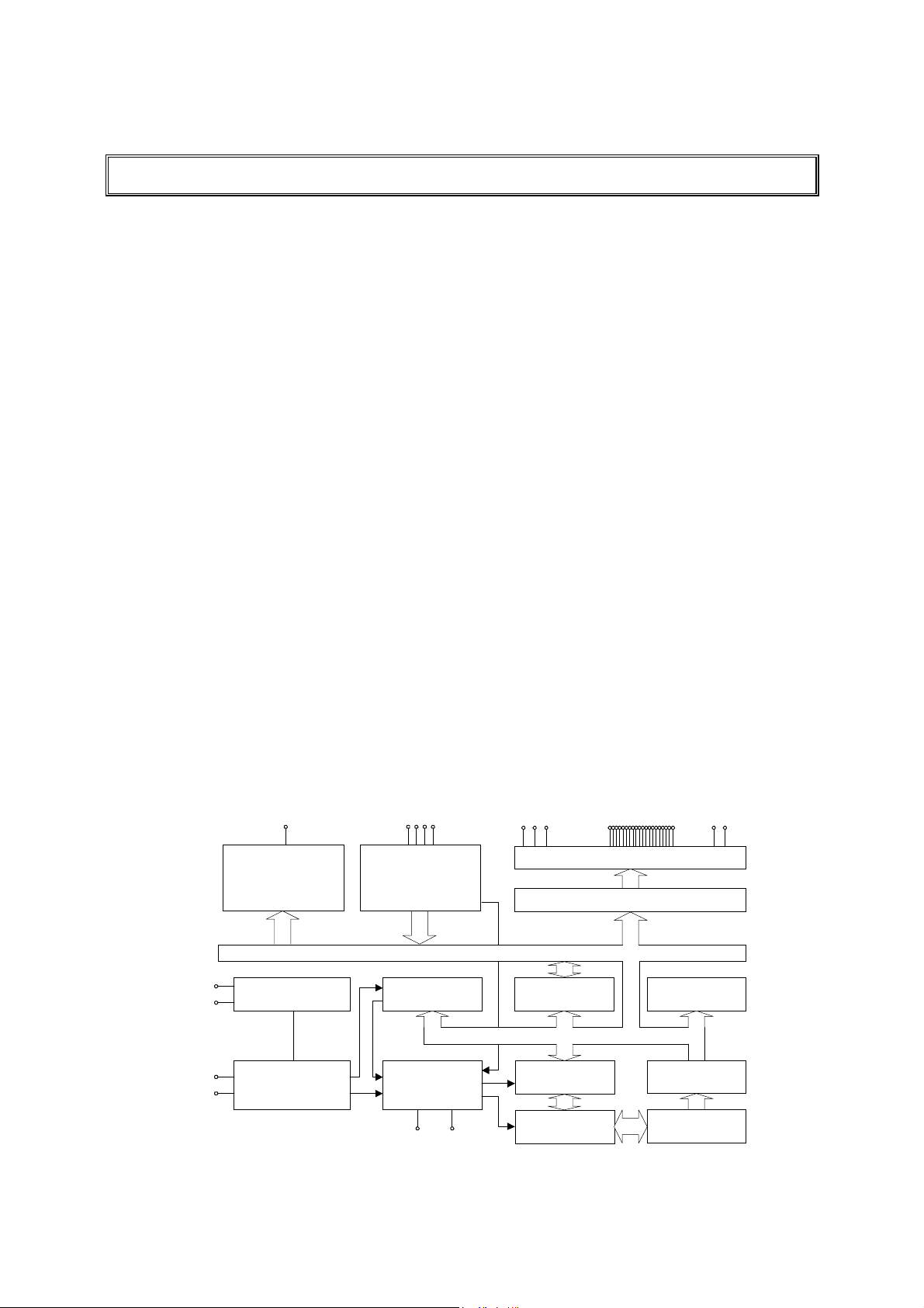
TheAPU4006 is a single-chip 4-bit microcontroller with LCD drivers. It can drive up to 3 common time
20 segments, i.e. 60 segments LCD driver. This 4-bit microcontroller contains a 4-bit parallel
processing ALU, 1024 x 15-bit program ROM, 48 x 4-bit data RAM, input ports, alarm driver, timer,
clock generator, crystal and RC oscillator circuit, LCD driver and 70 powerful instructions in a single
chip. It uses HALT instruction to stop all internal operations other than the timer, clock generator,
crystal/RC oscillator and LCD driver. Very low current dissipation can be easily achieved by
combining 4 types of interrupt function and HALT instruction to minimize the operation cycle.
BLOCK DIAGRAM
SEG1~20
LCD DIRVER
SEGMENT PLA
RAM 48 X 4 BITS
VDD1~2
OSC
IN
OSC
OUT
ALARM
OUTPUT
PORT
OSCILLATOR
M1~4
INPUT
PORT
4 BITS DATA BUS
6 BITS PRESET
TIMER
COM 1~3
ALU
CUP 1
CUP 2
PRE-DIVIDER
CONTROL
CIRCUIT
RESET
INT
1/8
10 BITS PROGRAM
COUNTER
4 LEVELS STACK
INSTRUCTION
DECODER
PROM
1024 X 15 BITS
Page 2
APLUS APU4006
1.0 PACKAGE & CHIP INFORMATION
Chip Size 1995 x 1590 (mm2)
Pad Pitch min. 140
Bounding Diagram
m
m
OSCIN
OSCOUT
TESTAM4M3
M2
M1
INTPAD
RESET
ALARM
VDD2
VDD1
VDD
CUP1
CUP2
COM1
SEG1
SEG2
SEG3
SEG4
SEG5
SEG6
2.0 PIN/PAD ASSIGNMENT
Unit : um
Pad
No.
1
2
3
4
5
6
7
8
9
10
11
12
Name
GND
VDD1
VDD2
ALARM
RESET
INT
M1
M2
M3
M4
TESTA
OSCOUT
Coordinate Coordinate
XY
1909.5 1128.60 21
1909.5 1275.60 22
1757.40 1500.60 23
1610.40 1500.60 24
1465.80 1500.60 25
1327.80 1500.60 26
1152.00 1500.60 27
1023.00 1500.60 28
894.00 1500.60 29
765.00 1500.60 30
636.00 1500.60 31
498.00 1500.60 32
SEG7
SEG8
SEG9
SEG10
SEG11
Pad
No.
SEG12
SEG13
Name
SEG4
SEG5
SEG6
SEG7
SEG8
SEG9
SEG10
SEG11
SEG12
SEG13
SEG14
SEG15
SEG14
SEG15
SEG16
XY
85.50 199.50
234.00 88.50
381.00 88.50
519.00 88.50
657.00 88.50
795.00 88.50
933.00 88.50
1071.00 88.50
1209.00 88.50
1347.00 88.50
1485.00 88.50
1623.00 88.50
GND
COM2
COM3
SEG20
SEG19
SEG18
SEG17
2/8
Page 3
APLUS APU4006
13
14
15
16
17
18
19
20
OSCIN
VDD
CUP1
CUP2
COM1
SEG1
SEG2
SEG3
155.10 1500.60 33
85.50 1132.50 34
85.50 994.50 35
85.50 865.50 36
85.50 736.50 37
85.50 607.50 38
85.50 478.50 39
85.50 349.50
SEG16
SEG17
SEG18
SEG19
SEG20
COM3
COM2
1761.00 88.50
1909.50 219.60
1909.50 375.60
1909.50 527.10
1909.50 678.60
1909.50 830.10
1909.50 981.60
*Note: The substrate must connect to GND.
3.0 PIN DESCRIPTION
Name Type Description
OSCIN
OSCOUT
M1 - 4 I Input pins with pull-down Tr or "L-level hold" Tr.
INT I External interrupt request control input pin.
RESET I System reset pin with pull-down resistance.
ALARM O
VDD
VDD1 For Ag-B mode positive power supply pin.
VDD2 For Li-B(EXTV) mode positive power supply pin.
GND Negative power supply pin.
CUP1 - 2 O Pins for connecting voltage step-up (step-down) capacitor.
I
Typical 32.768kHz crystal is connected across OSCIN/OSCOUT for
O
oscillation, R/C oscillation mode is also available.
Output only for outputting 4kHz/2kHz/1kHz modulation signal. Also can be
used to output non-modulation signal.
Power supply pin for logic unit inside LSI. When using Li version, a
capacitor must be connected across GND and VDD to prevent logic unit
from malfunctioning.
Output pins for LCD panel common plate.
The following pins are used in each case.
COM1 - 3
Static 1/2 duty 1/3 duty
O
COM1
COM2
COM3
Alternating
frequency
O
¾
¾
32Hz*
* Frequency can be doubled, quadrupled with PLA.
SEG1 - 20
Output pins for LCD panel segments.
O
* Also used as output ports with mask option.
TESTA * Test pin (for internal testing only).
3/8
O
O
¾
32Hz*
O
O
O
43Hz*
Page 4

APLUS APU4006
4.0 ABSOLUTE MAXIMUM RATINGS
at Ta = 0 to 70oC, GND = 0V
Name Symbol Range Unit
Maximum Supply Voltage
Maximum Input Voltage Vin1 -0.3 to VDD1+0.3 V
Maximum Output Voltage
Maximum Operating Temperature Topg 0 to +70
Maximum Storage Temperature Tstg -25 to +125
5.0 ALLOWABLE OPERATING CONDITIONS
at Ta = 0 to 70oC, GND = 0V
Name Symb. Condition Min. Max. Unit
VDD1 1.5 5.25 VSupply Voltage
VDD2
VDD1 1.2 5.25 VSupply Voltage
VDD2
Vss1 1.2V VOscillator Start-Up
Supply Voltage
Input "H" Voltage Vih1 VDD1-0.3 VDD1+0.3 V
Input "L" Voltage Vil1
Input "H" Voltage Vih2 VDD2-0.6 VDD2+0.6 V
Input "L" Voltage Vil2
Input "H" Voltage Vih3 0.8 x VDD1 VDD1 V
Input "L" Voltage Vil3
Input "H" Voltage Vih4 0.8 x VDD2 VDD2 V
Input "L" Voltage Vil4
Operating Freq.
Vss2
Fopg1
Fopg2
Fopg3
External RC Mode
Crystal Mode
Crystal Mode
Ag Battery Mode
Li Battery Mode
OSCIN at Ext. RC & Ag
Battery Mode
OSCIN at Ext. RC & Li
Battery Mode
Ag Battery Mode
Li Battery Mode
External RC Mode
VDD1 +1.3 to +5.5 V
VDD2 +2.5 to +5.5 V
Vout1 -0.3 to VDD1+0.3 V
Vout2 -0.3 to VDD2+0.3 V
o
o
3.5 5.25 V
2.4 5.25 V
1.2V V
-0.5 0.2 V
-0.7 0.7 V
0 0.2 x VDD1 V
0 0.2 x VDD2 V
32 32 KHz
32 100 KHz
32 1000 KHz
C
C
6.0 ELECTRICAL CHARACTERISTICS
at #1 : VDD1 = 1.2V ( Ag ); #2 : VDD2 = 2.4V ( Li ); #3 : VDD2 = 4V (ExtV).
6.1 Input Resistance
Name Symb. Condition Min. Typ. Max. Unit
M-Port L-Level Hold Tr
M-Port Pull-Down Tr
INT Pull-Up Tr
Rllh1
Rllh2
Rllh3
Rmsd1
Rmsd2
Rmsd3
Rintu1
Vi = 0.2VDD1, #1
Vi = 0.2VDD1, #2
Vi = 0.2VDD1, #3
Vi = VDD1, #1
Vi = VDD2, #2
Vi = VDD2, #3
Vi = VDD1, #1
4/8
10 40 100 Kohm
10 40 100 Kohm
200 700 2000 Kohm
200 500 1000 Kohm
100 250 500 Kohm
200 700 2000 Kohm
5 20 50 Kohm
Page 5

APLUS APU4006
Rintu2
Rintu3
Rintd1
INT Pull-Down Tr
RES Pull-Down R
6.2 DC Output Characteristics
Name Symb. Condition for Min. Typ. Max. Unit
Output "L" Voltage
6.3 Segment Driver Output Characteristics
Rintd2
Rintd3
Rres1
Rres2
Rres3
Voh1a
Voh2a
Voh3a
Vol1a
Vol2a
Vol3a
Vi = VDD2, #2
Vi = VDD2, #3
Vi = GND, #1
Vi = GND, #2
Vi = GND, #3
Vi = GND or VDD1, #1
Vi = GND or VDD2, #2
Vi = GND or VDD2, #3
Ioh = 200mA, #1
Ioh = 500mA, #2
Ioh = 1mA, #3
Iol = 400mA, #1
Iol = 1mA, #2
Iol = 2mA, #3
200 500 1000 Kohm
100 250 500 Kohm
200 700 2000 Kohm
200 500 1000 Kohm
100 250 500 Kohm
5 20 50 Kohm
5 20 50 Kohm
5 20 50 Kohm
0.8 0.9 1.0 V
1.5 1.8 2.1 VOutput "H" Voltage
Alarm
2.5 3 3.5 V
0.2 0.3 0.4 V
0.3 0.6 0.9 V
0.5 1 1.5 V
Name Symb. Condition for Min. Typ. Max. Unit
Output "H" Voltage
Output "L" Voltage
Output "H" Voltage
CMOS Output Mode
Voh1c
Voh2c
Voh3c
Vol1c
Vol2c
Vol3c
Voh1d
Voh2d
Voh3d
Vol1d
Vol2d
Vol3d
Voh1e
Voh2e
Voh3e
Vol1e
Vol2e
Vol3e
Duplex (1/2 Bias, 1/2 Duty) Display Mode
Voh12f
Voh3f
Vol12f
Vol3f
Voh12g
Voh3g
Ioh = -10uA, #1
Ioh = -50uA, #2
Ioh = -200uA, #3
Iol = 20uA, #1
Iol = 100uA, #2
Iol = 400uA, #3
Static Display Mode
Ioh = -1uA, #1
Ioh = -1uA, #2
Ioh = -1uA, #3
Iol = 1uA, #1
Iol = 1uA, #2
Iol = 1uA, #3
Ioh = -10uA, #1
Ioh = -10uA, #2
Ioh = -10uA, #3
Iol = 10uA, #1
Iol = 10uA, #2
Iol = 10uA, #3
Ioh = -1uA, #1, #2
Ioh = -1uA, #3
Iol = 1uA, #1, #2
Iol = 1uA, #3
Ioh = -10uA, #1, #2
Ioh = -10uA, #3
SEGn
SEGn
COMn
SEGn
COMn
0.8 0.9 1.0 V
1.5 1.8 2.1 VOutput "H" Voltage
2.5 3 3.5 V
0.2 0.3 0.4 V
0.3 0.6 0.9 VOutput "L" Voltage
0.5 1 1.5 V
1.0 V
2.2 VOutput "H" Voltage
3.8 V
0.2 V
0.2 VOutput "L" Voltage
0.2 V
1.0 V
2.2 VOutput "H" Voltage
3.8 V
0.2 V
0.2 VOutput "L" Voltage
0.2 V
2.2 V
3.8 V
0.2 V
0.2 V
2.2 V
3.8 V
5/8
Page 6

APLUS APU4006
Output "M" Voltage
Output "L" Voltage
Vom12g
Vom3g
Vol12g
Vol3g
Iol/h= +/-10uA, #1, #2
Iol/h= +/-10uA, #3
Iol = 10uA, #1
Iol = 10uA, #3
1.0 1.4 V
1.8 2.2 V
0.2 V
0.2 V
1/2 Bias, 1/3 Duty Display Mode
Output "H" Voltage
Output "L" Voltage
Output "H" Voltage
Output "M" Voltage
Output "L" Voltage
Voh12h
Voh3h
Vol12h
Vol3h
Voh12i
Voh3i
Vom12i
Vom3i
Vol12i
Vol3i
Ioh = -1uA, #1 ,#2
Ioh = -1uA, #3
Iol = 1uA, #1 ,#2
Iol = 1uA, #3
Ioh = -10uA, #1, #2
Ioh = -10uA, #3
Iol/h= +/-10uA, #1, #2
Iol/h= +/-10uA, #3
Iol = 10uA, #1, #2
Iol = 10uA, #3
SEGn
COMn
0.2 V
0.2 V
2.2 V
3.8 V
1.0 1.4 V
1.8 2.2 V
0.2 V
0.2 V
V
V
6.4 Instruction Table
Note: Rx=28~37 not used
Instruction Machine Code Function Remark Flag
NOP
LCT Y,X
MRA X
LCB Y,X
LCP Y,X
ADC X
ADC* X
SBC X
SBC* X
ADD X
ADD* X
SUB X
SUB* X
ADN X
ADN* X
AND X
AND* X
EOR X
EOR* X
OR X
OR* X
ADCI Y,D
ADCI* Y,D
SBCI Y,D
SBCI* Y,D
ADDI Y,D
ADDI* Y,D
SUBI Y,D
SUBI* Y,D
ADNI Y,D
ADNI* Y,D
000 0000 0000 0000
000 00YY YYXX XXXX
000 1101 01XX XXXX
000 01YY YYXX XXXX
000 10YY YYXX XXXX
001 0000 00XX XXXX
001 0000 10XX XXXX
001 0001 00XX XXXX
001 0001 10XX XXXX
001 0010 00XX XXXX
001 0010 10XX XXXX
001 0011 00XX XXXX
001 0011 10XX XXXX
001 0100 00XX XXXX
001 0100 10XX XXXX
001 0101 00XX XXXX
001 0101 10XX XXXX
001 0110 00XX XXXX
001 0110 10XX XXXX
001 0111 00XX XXXX
001 0111 10XX XXXX
001 1000 0DDD DYYY
001 1000 1DDD DYYY
001 1001 0DDD DYYY
001 1001 1DDD DYYY
001 1010 0DDD DYYY
001 1010 1DDD DYYY
001 1011 0DDD DYYY
001 1011 1DDD DYYY
001 1100 0DDD DYYY
001 1100 1DDD DYYY
No Operation
(Ly) <= (Rx) Y=000- No Use
CF <= (Rx3)
(Ly) <= (Rx) Y=000- No Use
abcd,efgh <= (Rx),(AC) Y=000- No Use
(AC) <= (Rx)+(AC)+(CF) CF
(AC),(Rx) <= (Rx)+(AC)+(CF) CF
(AC) <= (Rx)+(AC)B+(CF) CF
(AC),(Rx) <= (Rx)+(AC)B+(CF) CF
(AC) <= (Rx)+(AC) CF
(AC),(Rx) <= (Rx)+(AC) CF
(AC) <= (Rx)+(AC)B+1 CF
(AC),(Rx) <= (Rx)+(AC)B+1 CF
(AC) <= (Rx)+(AC)
(AC),(Rx) <= (Rx)+(AC)
(AC) <= (Rx) AND (AC)
(AC),(Rx) <= (Rx) AND (AC)
(AC) <= (Rx) EOR (AC)
(AC),(Rx) <= (Rx) EOR (AC)
(AC) <= (Rx) OR (AC)
(AC),(Rx) <= (Rx) OR (AC)
(AC) <= (Ry)+(D)+(CF) CF
(AC),(Ry) <= (Ry)+(D)+(CF) CF
(AC) <= (Ry)+(D)B+(CF) CF
(AC),(Ry) <= (Ry)+(D)B+(CF) CF
(AC) <= (Ry)+(D) CF
(AC),(Ry) <= (Ry)+(D) CF
(AC) <= (Ry)+(D)B+1 CF
(AC),(Ry) <= (Ry)+(D)B+1 CF
(AC) <= (Ry)+(D)
(AC),(Ry) <= (Ry)+(D)
6/8
Page 7

APLUS APU4006
Instruction Machine Code Function Remark Flag
ANDI Y,D
ANDI* Y,D
EORI Y,D
EORI* Y,D
ORI Y,D
ORI* Y,D
MRW Y,X
MWR X,Y
LDS X,D
IPM X
MAF X
MSB X
MSC X
STA X
SR0 X
SR1 X
SL0 X
SL1 X
LDA X
JB0 X
JB1 X
JB2 X
JB3 X
JNZ X
JNC X
JZ X
JC X
JMP X
CALL X
RTS
SMS X
TMS X
SF X
RF X
001 1101 0DDD DYYY
001 1101 1DDD DYYY
001 1110 0DDD DYYY
001 1110 1DDD DYYY
001 1111 0DDD DYYY
001 1111 1DDD DYYY
011 100Y YYXX XXXX
011 110Y YYXX XXXX
010 01DD DDXX XXXX
010 0000 10XX XXXX
011 0001 00XX XXXX
010 0010 00XX XXXX
011 0000 00XX XXXX
010 0010 10XX XXXX
010 0011 00XX XXXX
010 0011 01XX XXXX
010 0011 10XX XXXX
010 0011 11XX XXXX
011 0111 10XX XXXX
100 00XX XXXX XXXX
100 01XX XXXX XXXX
100 10XX XXXX XXXX
100 11XX XXXX XXXX
101 00XX XXXX XXXX
101 01XX XXXX XXXX
101 10XX XXXX XXXX
101 11XX XXXX XXXX
110 00XX XXXX XXXX
110 01XX XXXX XXXX
110 1000 0000 0000
111 0000 000X 0000
111 0010 00XX XXXX
111 0100 0X00 00XX
111 0110 0X00 00XX
(AC) <= (Ry) AND (D)
(AC),(Ry) <= (Ry) AND (D)
(AC) <= (Ry) EOR (D)
(AC),(Ry) <= (Ry) EOR (D)
(AC) <= (Ry) OR (D)
(AC),(Ry) <= (Ry) OR (D)
(AC),(Ry) <= (Rx)
(AC),(Rx) <= (Ry)
(AC),(Rx) <= (D)
(AC),(Rx) <= Port(M)
(AC),(Rx) <= STS1 TF2 : ZERO
TF3 : CF
(AC),(Rx) <= STS2 B0 : BCF
B1 :
SCF1(MPT)
B2 : SCF2(HRF)
(AC),(Rx) <= STS3 B0 : SCF4(INT)
B1 :
SCF5(TMR)
B2 : PH15
B3 : SCF7(PDV)
(Rx) <= (AC)
(ACn),(Rxn)
(AC3),(Rx3)
(ACn),(Rxn)
(AC3),(Rx3)
(ACn),(Rxn)
(AC0),(Rx0)
(ACn),(Rxn)
(AC0),(Rx0)
<= (Rxn+1)
<= 0
<= (Rxn+1)
<= 1
<= (Rxn-1)
<= 0
<= (Rxn-1)
<= 1
(AC) <= (Rx)
(PC) <= X if (AC0) = 1
(PC) <= X if (AC1) = 1
(PC) <= X if (AC2) = 1
(PC) <= X if (AC3) = 1
(PC) <= X
if AC ¹ 0
(PC) <= X if (CF) = 0
(PC) <= X if AC = 0
(PC) <= X if (CF) = 1
(PC) <= X
(STACK)
(PC)
<= (PC)+1
<= X
(PC) <= (STACK)
SEF4 <= X4 M1-4 Enable HRF0
TIMER <= X HRF1
X6
X1
X0
X6
X1
X0
: M-PORT Pull-Low
: BCF Set
: CF Set
: M-PORT Low-L-H
: BCF Reset
: CF Reset
BCF
CF
7/8
Page 8

APLUS APU4006
Instruction Machine Code Function Remark Flag
ALM X
SIE X
SIE* X
PLC X
HALT
6.5 Symbol Description
AC : Accumulator CF : Carry Flag
ACn : Accumulator Bit N BCF : Backup Flag
Rx : Memory of Address X IEFn : Interrupt Enable Flag
Rxn : Memory Bit N of Address X HEFn : Halt Release Enable Flag
Ry : Memory of Working Register Y HRFn : Halt Release Flag
D : Immediate Data SCFn : Start Condition Flag
PC : Program Counter Ly : LCD Latch
111 0111 XXXX XXXX
111 1000 XXXX XXXX
111 1010 0000 XXXX
111 110X XXXX XXXX
111 1111 1111 1111
X7,X6 0 , 1 1 , 0 1 , 1
Signal DC 1K/2K 4K Hz
Xn = 1 X5 X4 X3
Signal 1 Hz 2 Hz 4 Hz
Xn = 1 X2 X1 X0
Signal 8 Hz 16 Hz 32 Hz
X5-7
X0-3
X0-3 : IEF0-3 is Enabled
X0-3
X8
: HEF1-3 is Enabled
: IEF0-3 is Enabled
: Reset HRF0-3
: Reset PH11-15
8/8
 Loading...