

Page 1
4-Bit Micro-Controller With EPROM, 1K Word
APU4003T
Features
y Very low current dissipation.
y Wide operating voltage range.
y Supports both Ag and Li batteries.
y Powerful instruction set.
y 4-level subroutine nesting
(including interrupt).
y 4 event-driven interrupts, 2 external and 2
internal.
y ROM size: 1024x15 bits.
y RAM size: 64x4 bits.
y Input ports: 2 ports/ 8 pins (S and M).
y Output port: 1 port/ 4 pins (P).
y Pseudo serial output port (P).
y Input/Output ports: 2 ports/ 8 pins
(I/OA and I/OB).
General Description
The APU4003T is an EEPROM-equipped high- performance 4-bit microcomputer.
It contains not only all functions compatible with APU4003T, but also an EEPROM, providing customers such
conveniences as on-board verification,
y Control outputs: ALARM, LIGHT.
y LCD driver outputs
(can drive up to 75 LCD segments).
y PROM option to select 4 LCD drive modes:
static, duplex (1/2 duty 1/2 bias, 1/3 duty 1/2 bias
or 1/3 duty 1/3 bias).
y PROM option permits LCD driver output pins to
be used for DC output ports; up to 25 pins are
available.
y Segment PLA circuit permits any layout on LCD
panel.
y Built-in clock generator (crystal or RC).
y Built-in voltage doubler, halver, tripler.
y Endurance: More then 100 write cycles/word.
y Security bit for read/write protection.
customized code, small quantity sample production, etc.
This chip especially provides a security bit to protect the customer’s code.
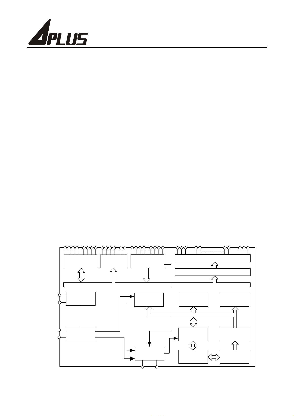
Block Diagram
$ODUP
3a
2XWSXW3RUW
/LJKW
6a 0a
,QSXW3RUW
%LW'DWD%XV
%LW3UHVHW
7LPHU
&RQWURO
&LUFXLW
&20a
/HYHO6WDFN
%LW3URJUDP
26&,1
26&287
&83
&83
,2
$a
%LGLUHFWLRQ
,2SRUW
2VFLOODWRU
3UH'LYLGHU
,2
%a
$/8
&RXQWHU
6(*a6(*
/&''ULYHU
6HJPHQW3/$
5$0[%LWV
9''a
,QVWUXFWLRQ
'HFRGHU
3520
[%LW
Preliminary
5(6(7 ,17
1 Ver.0.0
Page 2
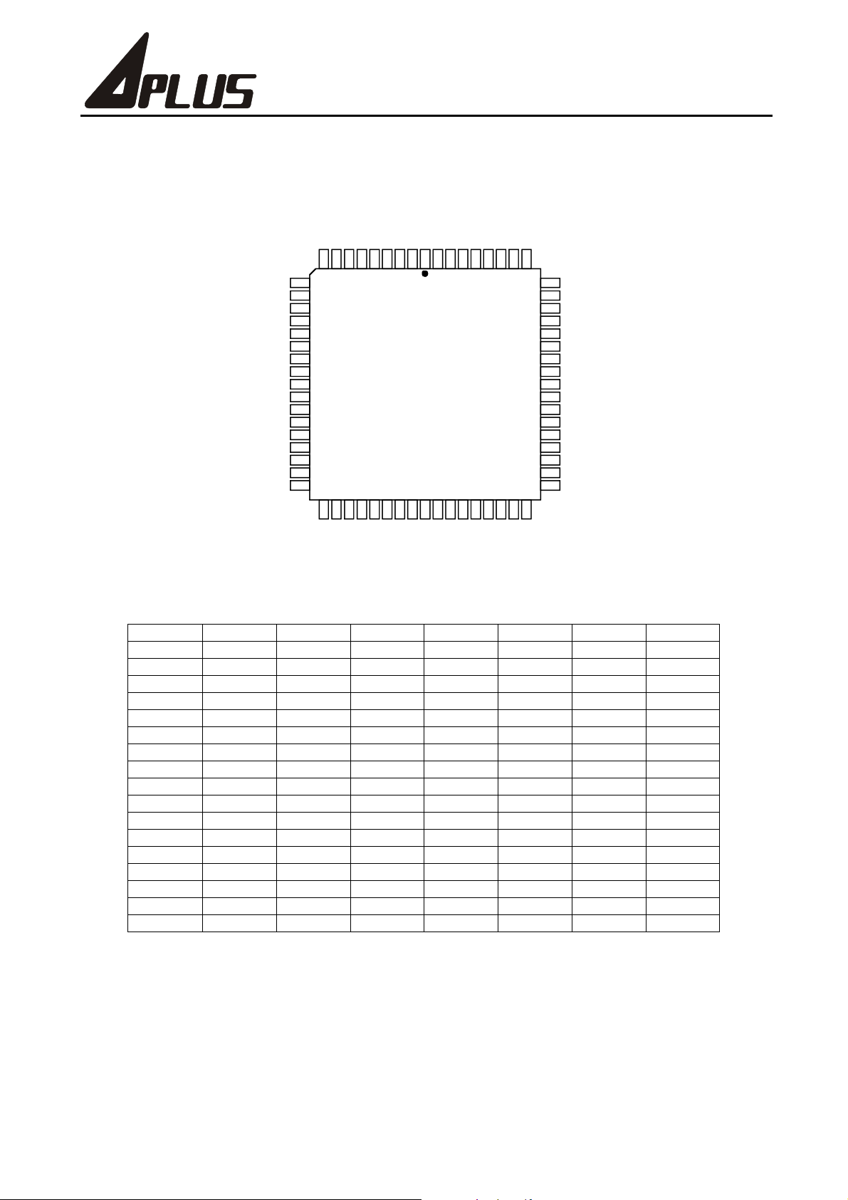
Package Information
APU4003T
Package type 68Pin PLCC
S3S4LIGHT
ALARM
VDD2
VDD
VDD1
GND
VDD3
COM2
COM3
SEG25
SEG24
SEG23
IOA1
IOA2
IOA3
IOA4
IOB1
IOB2
IOB3
IOB4
RESET
INT
P1
P2
P3
P4
M1
M2
M3
10
15
20
25
M4
5
30
TEST A
CUP1
68
APU4003T
35
S2
S1
CUP2
CAP
OSCIN
65
40
SEG1
COM1
OSCOUT
SEG2
SEG3
60
55
50
45
SEG4
SEG5
SEG22
SEG21
SEG20
SEG19
SEG18
SEG17
SEG16
SEG15
SEG14
SEG13
SEG12
SEG11
SEG10
SEG9
SEG8
SEG7
SEG6
Pin/Pad Assignment Unit: Pm
Pin No. Name Pin No. Name Pin No. Name Pin No. Name
1 VSS 18 RESET 35 OSCIN 52 SEG14
2 ------ 19 INT 36 CAP 53 SEG15
3 VDD1 20 P1 37 OSCOUT 54 SEG16
4 VDD 21 P2 38 COM1 55 SEG17
5 VDD2 22 P3 39 SEG1 56 SEG18
6 ALARM 23 P4 40 SEG2 57 SEG19
7 LIGHT24 M1 41SEG358SEG20
8 S4 25 M2 42SEG459SEG21
9 S3 26 M3 43SEG560SEG22
10 IOA1 27 M4 44 SEG6 61 -----11 IOA2 28 ------ 45 SEG7 62 -----12 IOA3 29 ------ 46 SEG8 63 SEG23
13 IOA4 30 TESTA 47 SEG9 64 SEG24
14 IOB1 31 CUP1 48 SEG10 65 SEG25
15 IOB2 32 CUP2 49 SEG11 66 COM3
16 IOB3 33 S2 50 SEG12 67 COM2
17 IOB4 34 S1 51 SEG13 68 VDD3
Preliminary
2 Ver.0.0
Page 3
Pin Name Description
APU4003T
Name Type Description
OSCIN
OSCOUTIO
S1~4 I
M1~4 I
Typical crystal(32.768KHz) is connected across
OSCIN/OSCOUT for oscillation; R/C oscillation mode is also available.
Input ports with chattering eliminator option for CK10 (32ms), CK8 (8ms) &
CK6 (2ms).
P1~4 O Output ports.
IOA1~4 I/O Input/Output ports.
IOB1~4 I/O Input/Output ports.
INT I External interrupt request control input pin.
RESET I System reset pin.
LIGHT O Output only for outputting the signal to drive the transistor for light.
ALARM O Output only for outputting the 4kHz/2kHz/1kHz modulation signal.
Also can be used to output the non-modulation signal.
VDD
VDD1
(+)Power supply pin.
* For Ag version, apply (+) side to VDD & VDD1 together.
VDD2 For other than Ag version, apply (+) side to VDD & VDD2 together.
VDD3 Power supply pin for LCD driver power supply.
VSS (--)Power supply pin.
CUP1~2 O Pins for connecting the voltage step-up (step-down) capacitor.
COM1~3 O Output pins for LCD panel common plate.
SEG1~25 O Output pins for LCD panel segments.
Absolute Maximum Rating Ta = 0 to 70к
Name Symbol Rating Unit
Maximum Supply Voltage
V
V
Maximum Input Voltage V
V
Maximum Output Voltage
V
V
Maximum Operating Temperature t
Maximum Storage Temperature t
SS1/2
SS3
IN1
OUT1
OUT2
OUT3
OPG
STG
-0.3 ~ +5.5 V
-0.3 ~ +8.5 V
-0.3 to VDD+0.3 V
-0.3 to V
-0.3 to V
-0.3 to V
+0.3 V
DD1
+0.3 V
DD2
+0.3 V
DD3
0 to +70
-25 to +125
к
к
Allowable operating conditions Ta = 0 to 70к
Supply Voltage
Supply Voltage
Input sHs Voltage
Input sLs Voltage
Input sHs Voltage
Input sLs Voltage
Operating Freq.
Preliminary
Name Symbol Condition Min. Max. Unit
V
DD1
V
DD2
V
DD3
V
DD1
V
DD2
V
DD3
V
V
V
V
f
OPG1
f
OPG2
f
OPG3
f
OPG4
External Voltage
Mode
Ag & Li Battery
Mode
IH1
All Input Except OSCIN
IL1
IH2
OSCIN at Ext. RC Mode
IL2
Ag Battery Mode 32 32 kHz
Li Battery Mode 32 100 kHz
External Voltage Mode 32 3580 kHz
External RC Mode 32 5000 kHz
2.0 5.5 V
4.0 5.5 V
4.0 8.25 V
1.3 5.5 V
2.6 5.5 V
2.6 8.25 V
0.7V
DDO
00.3V
0.8V
DDO
00.2V
V
DDO
DDO
V
DDO
DDO
V
V
V
V
3 Ver.0.0
Page 4

Electrical Characteristics Ta=0 to 70к
APU4003T
Input resistance
Name Symbol Condition Min. Typ. Max. Unit
sLs-Level Hold t
M/S Pull-Down t
INT Pull-Up t
R
INT Pull-Down t
RES Pull-Down t
R
IIH1
R
R
R
R
R
R
R
R
R
R
R
R
R
R
MSD1
MSD2
MSD3
INTU1
INTU2
INTU3
INTD1
INTD2
INTD3
RES1
RES2
RES3
IIH2
IIH3
R
R
R
R
VI=0.2V
VI=0.2V
VI=0.3V
VI=V
VI=V
VI=V
, #1 10 40 100
DD1
, #2 10 40 100
DD2
, #3 5 20 50
DD2
, #1 200 500 1000
DD1
, #2 200 500 1000
DD2
, #3 100 250 500
DD2
VI=VSS, #1 200 500 1000
VI=VSS, #2 200 500 1000
VI=VSS, #3 100 250 500
VI=V
VI=V
VI=V
VI=VDD or V
VI=VDD or V
VI=VDD or V
, #1 200 500 1000
DD1
, #2 200 500 1000
DD2
, #3 100 250 500
DD2
, #1 5 20 50
SS1
, #2 5 20 50
SS2
, #3 5 20 50
SS2
k:
k:
k:
k:
k:
k:
k:
k:
k:
k:
k:
k:
k:
k:
k:
Note: #1: V
= 1.3V (Ag), #2: V
DD1
= 2.6V (Li), #3: V
DD2
DC output characteristics
Name Symbol Condition For Min. Typ. Max. Unit
Output sHs Voltage
Output sLs Voltage
Output sHs Voltage
Output sLs Voltage
Note: #1: V
= 1.3V (Ag), #2: V
DD1
V
OH1a
V
OH2 aIOH
V
OH3 aIOH
V
OL1 a
V
OL2 aIOL
V
OL3 aIOL
V
OH1b
V
OH2b
V
OH3bIOH
V
OL1b
V
OL2b
V
OL3b
DD2
IOH=-200PA, #1
IOL=400PA, #1
IOH=-100PA, #1
IOH=-500PA, #2
IOL=200PA, #1
IOL=1mA, #2 0.6 1 V
IOL=3mA, #3
= 2.6V (Li), #3: V
Segment driver output characteristics
Name Symbol Condition For Min. Typ. Max. Unit
DC output mode
V
OH1c
Output sHs Voltage
Output sLs Voltage
V
V
V
V
V
OH2c
OH3c
OL1c
OL2c
OL3c
Static display mode
V
Output sHs Voltage
Output sLs Voltage
V
V
V
OH2d
OH3d
OL2d
OL3d
= 4.5V (ExtV).
DD2
0.9 1.1 V
=-1ma, #2 1.8 2.1 V
=-3mA, #3
Alarm
Light
3.0 3.5 V
0.3 0.5 V
=2mA, #2 0.6 1 V
=6mA, #3 1.0 1.5 V
P-port
IOA-n
=-1.5mA, #3 3.0 3.5 V
IOB-n
0.9 1.1 V
1.8 2.1 V
0.3 0.5 V
1.0 1.5 V
= 4.5V (ExtV).
DD2
IOH=-10PA, #1
IOH=-50PA, #2
IOH=-200PA, #3
IOL=20PA, #1
IOL=100PA, #2
IOL=400PA, #3
IOH=-1PA, #1, #2
IOH=-1PA, #3
I
=1PA, #1, #2
OL
I
=1PA, #3
OL
SEG-n
SEG-n
0.9 1.1 V
1.8 2.1 V
3.0 3.5 V
0.3 0.5 V
0.6 1 V
1.0 1.5 V
2.5 V
4.3 V
0.2 V
0.2 V
Preliminary
4 Ver.0.0
Page 5

Name Symbol Condition For Min. Typ. Max. Unit
APU4003T
Output sHs Voltage
Output sLs Voltage
V
V
V
V
OH2e
OH3e
OL2e
OL3e
IOH=-10PA,#1, #2
IOH=-10PA, #3
I
=10PA, #1, #2
OL
IOL=10PA, #3
Duplex (1/2 bias, 1/2 duty) display mode
Output sHs Voltage
Output sLs Voltage
Output sHs Voltage
Output sMs Voltage
Output sLs Voltage
V
V
V
V
V
V
V
V
V
V
OH12f
OH3f
OL12f
OL3f
OH12g
OH3g
OM12g
OM3g
OL12g
OL3g
IOH=-1PA, #1, #2
IOH=-1PA, #3
I
=1PA, #1, #2
OL
IOL=1PA, #3
IOH=-10PA, #1, #2
I
=-10PA, #3
OH
I
=r10PA,#1,
OI/H
#2
I
=r10PA, #3
OI/H
IOL=10PA, #1
IOL=10PA, #3
1/2 bias, 1/3duty display mode
Output sHs Voltage
Output sLs Voltage
Output sHs Voltage
Output sMs Voltage
Output sLs Voltage
V
V
V
V
V
V
V
V
V
V
OH12h
OH3h
OL12h
OL3h
OH12i
OH3i
OM12i
OM3i
OL12i
OL3i
IOH=-1PA, #1, #2
IOH=-1PA, #3
IOL=1PA, #1, #2
IOL=1PA, #3
IOH=-10PA, #1, #2
IOH=-10PA, #3
I
=r10PA,#1,
OI/H
#2
I
=r10PA, #3
OI/H
IOL=10PA, #1, #2
IOL=10PA, #3
1/3bias, 1/3duty display mode
Output sHs Voltage
Output sM1s Voltage
Output sM2s Voltage
Output sLs Voltage
Output sHs Voltage
Output sM1s Voltage
Output sM2s Voltage
Output sLs Voltage
V
V
V
V
V
V
V
V
V
V
V
OM12k
V
OM13k
V
OM22k
V
OM23k
V
V
OH12j
OH3j
OM12j
OM13j
OM22j
OM23j
OL2j
OL3j
OH2k
OH3k
OL2k
OL3k
IOH=-1PA, #1, #2
IOH=-1PA, #3
I
=r1PA,#1, #2
OI/H
I
=r1PA,#1, #2
OI/H
I
=r1PA,#1, #2
OI/H
I
=r1PA,#1, #2
OI/H
IOL=1PA, #2
IOL=1PA, #3
IOH=-10PA, #2
IOH=-10PA, #3
I
=r10PA,#1,
OI/H
#2
I
=r10PA, #3
OI/H
I
=r10PA,#1,
OI/H
#2
I
=r10PA, #3
OI/H
IOL=10PA, #2
IOL=10PA, #3
COM-n
SEG-n
COM-n
SEG-n
COM-n
SEG-n
COM-n
2.5 V
4.3 V
0.2 V
0.2 V
2.4 V
4.3 V
0.2 V
0.2 V
2.4 V
4.3 V
1.1 1.5 V
2.05 2.45 V
0.2 V
0.2 V
2.4 V
4.3 V
0.2 V
0.2 V
2.4 V
4.3 V
1.1 1.5 V
2.05 2.45 V
0.2 V
0.2 V
3.85 V
6.55 V
2.9 2.4 V
4.7 4.3 V
1.1 1.5 V
2.05 2.45 V
0.2 V
0.2 V
3.85 V
6.55 V
2.9 2.4 V
4.7 4.3 V
1.1 1.5 V
2.05 2.45 V
0.2 V
0.2 V
Note: #1: V
SS1
Preliminary
= -1.2V (Ag), #2: V
= -2.4V (Li), #3: V
SS2
= -4V (ExtV).
SS2
5 Ver.0.0
Page 6

Instruction Table
APU4003T
Instruction Machine Code Function Remark Flag
NOP 000 0000 0000 0000
LCT Ly,Rx 000 00YY YYXX XXXX
OPA Rx 000 0100 01XX XXXX
LCB Ly,Rx 000 01YY YYXX XXXX
OPB Rx 000 1000 01XX XXXX
LCP Ly,Rx 000 10YY YYXX XXXX
MRA Rx 000 1101 01XX XXXX
OPP Rx 000 1110 00XX XXXX
OPP S Rx 000 1110 1DXX XXXX
ADC Rx 001 0000 00XX XXXX
ADC* Rx 001 0000 10XX XXXX
SBC Rx 001 0001 00XX XXXX
SBC* Rx 001 0001 10XX XXXX
ADD Rx 001 0010 00XX XXXX
ADD* Rx 001 0010 10XX XXXX
SUB Rx 001 0011 00XX XXXX
SUB* Rx 001 0011 10XX XXXX
ADN Rx 001 0100 00XX XXXX
ADN* Rx 001 0100 10XX XXXX
AND Rx 001 0101 00XX XXXX
AND* Rx 001 0101 10XX XXXX
EOR Rx 001 0110 00XX XXXX
EOR* Rx 001 0110 10XX XXXX
OR Rx 001 0111 00XX XXXX
OR* Rx 001 0111 10XX XXXX
ADCI Ry,D 001 1000 0DDD DYYY
ADCI* Ry,D 001 1000 1DDD DYYY
SBCI Ry,D 001 1001 0DDD DYYY
SBCI* Ry,D 001 1001 1DDD DYYY
ADDI Ry,D 001 1010 0DDD DYYY
ADDI* Ry,D 001 1010 1DDD DYYY
SUBI Ry,D 001 1011 0DDD DYYY
SUBI* Ry,D 001 1011 1DDD DYYY
ADNI Ry,D 001 1100 0DDD DYYY
ADNI* Ry,D 001 1100 1DDD DYYY
ANDI Ry,D 001 1101 0DDD DYYY
ANDI* Ry,D 001 1101 1DDD DYYY
EORI Ry,D 001 1110 0DDD DYYY
EORI* Ry,D 001 1110 1DDD DYYY
ORI Ry,D 001 1111 0DDD DYYY
ORI* Ry,D 001 1111 1DDD DYYY
IPS Rx 010 0000 00XX XXXX
IPM Rx 010 0000 10XX XXXX
IPA Rx 010 0001 00XX XXXX
IPA* Rx 010 0001 01XX XXXX
IPB Rx 010 0001 10XX XXXX
No Operation
(Ly) m (Rx)
Port(A) m (Rx)
(Ly) m (Rx)
Port(B) m (Rx)
abcd,efgh m (Rx),(AC)
CF m Rx3
Port(P) m (Rx)
P1,2,3,4 m Rx0,Rx1,D,Pulse
(AC) m (Rx)+(AC)+(CF)
(AC),(Rx) m (Rx)+(AC)+(CF)
(AC) m (Rx)+(AC)B+(CF)
(AC),(Rx) m (Rx)+(AC)B+(CF)
(AC) m (Rx)+(AC)
(AC),(Rx) m (Rx)+(AC)
(AC) m (Rx)+(AC)B+1
(AC),(Rx) m (Rx)+(AC)B+1
(AC) m (Rx)+(AC)
(AC),(Rx) m (Rx)+(AC)
(AC) m (Rx) AND (AC)
(AC),(Rx) m (Rx) AND (AC)
(AC) m (Rx) EOR (AC)
(AC),(Rx) m (Rx) EOR (AC)
(AC) m (Rx) OR (AC)
(AC),(Rx) m (Rx) OR (AC)
(AC) m (Ry)+(D)+(CF)
(AC),(Ry) m (Ry)+(D)+(CF)
(AC) m (Ry)+(D)B+(CF)
(AC),(Ry) m (Ry)+(D)B+(CF)
(AC) m (Ry)+(D)
(AC),(Ry) m (Ry)+(D)
(AC) m (Ry)+(D)B+1
(AC),(Ry) m (Ry)+(D)B+1
(AC) m (Ry)+(D)
(AC),(Ry) m (Ry)+(D)
(AC) m (Ry) AND (D)
(AC),(Ry) m (Ry) AND (D)
(AC) m (Ry) EOR (D)
(AC),(Ry) m (Ry) EOR (D)
(AC) m (Ry) OR (D)
(AC),(Ry) m (Ry) OR (D)
(AC),(Rx) m Port(S)
(AC),(Rx) m Port(M)
(AC),(Rx) m Port(A)
(AC),(Rx) m Port(A)
(AC),(Rx) m Port(B)
Ly=000- No Use
Ly=000- No Use
LY=000- No Use
CF
CF
CF
CF
CF
CF
CF
CF
CF
CF
CF
CF
CF
CF
CF
CF
I/OA m I/P
Preliminary
6 Ver.0.0
Page 7

Instruction Machine Code Function Remark Flag
APU4003T
IPB* Rx 010 0001 11XX XXXX
MSB Rx 010 0010 00XX XXXX
STA Rx 010 0010 10XX XXXX
SR0 Rx 010 0011 00XX XXXX
SR1 Rx 010 0011 01XX XXXX
SL0 Rx 010 0011 10XX XXXX
SL1 Rx 010 0011 11XX XXXX
LDS Rx,D 010 01DD DDXX
XXXX
MSC Rx 011 0000 00XX XXXX
MAF Rx 011 0001 00XX XXXX
LDA Rx 011 0111 10XX XXXX
MRW
Ry,Rx
MWR
Rx,Ry
JB0 X 100 00XX XXXX XXXX
JB1 X 100 01XX XXXX XXXX
JB2 X 100 10XX XXXX XXXX
JB3 X 100 11XX XXXX XXXX
JNZ X 101 00XX XXXX XXXX
JNC X 101 01XX XXXX XXXX
JZ X 101 10XX XXXX XXXX
JC X 101 11XX XXXX XXXX
JMP X 110 00XX XXXX XXXX
CALL X 110 01XX XXXX XXXX
RTS 110 1000 0000 0000
SMS X 111 0000 000X XXXX
TMS X 111 0010 00XX XXXX
SF X 111 0100 0XX0 XXXX
011 100Y YYXX XXXX
011 110Y YYXX XXXX
(AC),(Rx) m Port(B)
(AC),(Rx) m STS2
(Rx) m (AC)
ACn, Rxn m Rx(n+1)
AC3, Rx3 m 0
ACn, Rxn m (Rx(n+1)
AC3, Rx3 m 1
ACn, Rxn m Rx(n-1)
AC0, Rx0 m 0
ACn, Rxn m Rx(n-1)
AC0, Rx0 m 1
(AC),(Rx) m (D)
(AC),(Rx) m STS3
(AC),(Rx) m STS1
(AC) m (Rx)
(AC),(Ry) m (Rx)
(AC),(Rx) m (Ry)
(PC) m X
(PC) m X
(PC) m X
(PC) m X
(PC) m X
(PC) m X
(PC) m X
(PC) m X
(PC) m X
(STACK) m (PC)+1
(PC m X
(PC) m (STACK)
SEF4 m X4
SEF0~3 m X0~3
TIMER m X
X6: M-PORT Pull-Low
X5: S-PORT Pull-Low
X3: HALT After Light
X2: LIGHT ON
X1: BCF Set
X0: CF Set
X6: M-PORT Low-L-H
X5: S-PORT Low-L-H
I/OB m I/P
B0: BCF
B1: SCF1(MPT)
B2: SCF2(HRF)
B3: SCF3(SPT)
B0: SCF4(INT)
B1: SCF5(TMR)
B2: PH15
B3: SCF7(PDV)
TF2: ZERO
TF3: CF
if (AC0)=1
if (AC1)=1
if (AC2)=1
if (AC3)=1
if (Zero)=0
if (CF)=0
if (Zero)=1
if (CF)=1
M1~4 Enable
S1~4 Enable
SCF1
SCF3
HRF0
HRF1
BCF
CF
Preliminary
7 Ver.0.0
Page 8

Instruction Machine Code Function Remark Flag
APU4003T
RF X 111 0110 0XX0 0XXX X2: LIGHT OFF
ALM X 111 0111 XXXX XXXX
SIE X 111 1000 XXX0 XXXX
SIE* X 111 1010 0000 XXXX X0~3: IEF0~3 is Enabled
PLC X 111 110X 0000 XXXX
HALT 111 1111 1111 1111
Symbol description
AC: Accumulator CF: Carry Flag
ACn: Accumulator Bit N BCF: Backup Flag
Rx: Memory of Address X IEFn: Interrupt Enable Flag
Rxn: Memory Bit N of Address X HEFn: HALT Release Enable Flag
Ry: Memory of Working Register Y HRFn: HALT Release Flag
PC: Program Counter SEFn: Switch Enable Flag
X: Address SCFn: Start Condition Flag
D: Immediate Data Ly: LCD Latch
X1: BCF Reset
X0: CF Reset
X7,X6 0,1 1,0 1,1
Signal DC 1K/2K 4K
Xn=1 X5 X4 X3
Signal 1Hz 2Hz 4Hz
Xn=1 X2 X1 X0
Signal 8Hz 16Hz 32Hz
X5~7: HEF1~3 is Enabled
X0~3: IEF0~3 is Enabled
X0~3: Reset HRF0~3
X8: Reset PH11~15
BCF
CF
Preliminary
8 Ver.0.0
 Loading...