

Page 1
"UL Recognized" File No. E145592 (S)
D
S
S
G
G
D
SOT-227
S
ISOTOP
®
POWER MOS IV
®
APT8018JN 800V 40A 0.18Ω
SINGLE DIE ISOTOP® PACKAGE
N-CHANNEL ENHANCEMENT MODE HIGH VOLTAGE POWER MOSFETS
MAXIMUM RATINGS All Ratings: TC = 25°C unless otherwise specified.
APT
Symbol
V
DSS
I
D
IDM, l
LM
V
GS
P
D
TJ,T
STG
T
L
Parameter
Drain-Source Voltage
Continuous Drain Current @ T
Pulsed Drain Current
Gate-Source Voltage
Total Power Dissipation @ T
Linear Derating Factor
Operating and Storage Junction Temperature Range
Lead Temperature: 0.063" from Case for 10 Sec.
1
= 25°C
C
and Inductive Current Clamped
= 25°C
C
8018JN
800
40
160
±30
690
5.52
-55 to 150
300
UNIT
Volts
Amps
Volts
Watts
W/°C
°C
STATIC ELECTRICAL CHARACTERISTICS
Symbol
BV
ID(ON)
R
DS
I
DSS
I
GSS
VGS(TH)
Characteristic / Test Conditions / Part Number
Drain-Source Breakdown Voltage
DSS
(V
= 0V, ID = 250 µA)
GS
On State Drain Current
(V
> ID(ON) x RDS(ON) Max, VGS = 10V)
DS
Drain-Source On-State Resistance
(ON)
(VGS = 10V, 0.5 ID [Cont.])
Zero Gate Voltage Drain Current (V
Zero Gate Voltage Drain Current (V
Gate-Source Leakage Current (V
Gate Threshold Voltage (V
2
= VGS, ID = 5.0mA)
DS
2
= V
DS
= 0.8 V
DS
= ±30V, V
GS
, VGS = 0V)
DSS
, VGS = 0V, TC = 125°C)
DSS
= 0V)
DS
MIN TYP MAX
APT8018JN
APT8018JN 40
APT8018JN 0.18
800
250
1000
±100
24
UNIT
Volts
Amps
Ohms
µA
nA
Volts
THERMAL CHARACTERISTICS
Symbol
R
R
USA
405 S.W. Columbia Street Bend, Oregon 97702-1035 Phone: (541) 382-8028 FAX: (541) 388-0364
EUROPE
Avenue J.F. Kennedy Bât B4 Parc Cadéra Nord F-33700 Merignac - France Phone: (33) 5 57 92 15 15 FAX: (33) 5 56 47 97 61
Characteristic
Junction to Case
ΘJC
Case to Sink
ΘCS
CAUTION: These Devices are Sensitive to Electrostatic Discharge. Proper Handling Procedures Should Be Followed.
(Use High Efficiency Thermal Joint Compound and Planer Heat Sink Surface.)
MIN TYP MAX
0.05
UNIT
0.18
°C/W
050-8038 Rev E
Page 2
DYNAMIC CHARACTERISTICS
APT8018JN
Symbol
C
C
C
Q
Q
Q
td(on)
td(off)
Characteristic
Input Capacitance
iss
Output Capacitance
oss
Reverse Transfer Capacitance
rss
Total Gate Charge
g
Gate-Source Charge
gs
Gate-Drain ("Miller") Charge
gd
Turn-on Delay Time
t
Rise Time
r
Turn-off Delay Time
t
Fall Time
f
Test Conditions
V
VDS = 25V
f = 1 MHz
3
V
GS
VDD = 0.5 V
ID = ID [Cont.] @ 25°C
V
GS
VDD = 0.5 V
ID = ID [Cont.] @ 25°C
RG = 0.6Ω
SOURCE-DRAIN DIODE RATINGS AND CHARACTERISTICS
I
SM
Characteristic / Test Conditions
Continuous Source Current
S
(Body Diode)
Pulsed Source Current
(Body Diode)
Diode Forward Voltage
SD
Reverse Recovery Time (I
rr
Reverse Recovery Charge (I
rr
1
2
(VGS = 0V, IS = -ID [Cont.])
= -ID [Cont.], dlS/dt = 100A/µs)
S
= -ID [Cont.], dlS/dt = 100A/µs)
S
Symbol
I
V
t
Q
MIN TYP MAX
GS
= 0V
11715 14000
1430 2000
460 690
= 10V
DSS
468 700
72 110
176 265
= 15V
DSS
21 40
19 40
70 105
13 25
MIN TYP MAX
APT8018JN
APT8018JN 160
945 1800
36 60
40
1.8
UNIT
pF
nC
ns
UNIT
Amps
Volts
ns
µC
PACKAGE CHARACTERISTICS
L
L
Characteristic / Test Conditions
Internal Drain Inductance
D
Internal Source Inductance (Measured From Source Terminals to Source Bond Pads)
S
(Measured From Drain Terminal to Center of Die.)
RMS Voltage (50-60 Hz Sinusoidal Waveform From Terminals to Mounting Base for 1 Min.)
Drain-to-Mounting Base Capacitance (f = 1MHz)
Maximum Torque for Device Mounting Screws and Electrical Terminations.
0.2
D=0.5
0.1
, THERMAL IMPEDANCE (°C/W)
JC
θ
Z
0.05
0.01
0.005
0.001
0.0005
0.2
0.1
0.05
0.02
0.01
SINGLE PULSE
-5
10
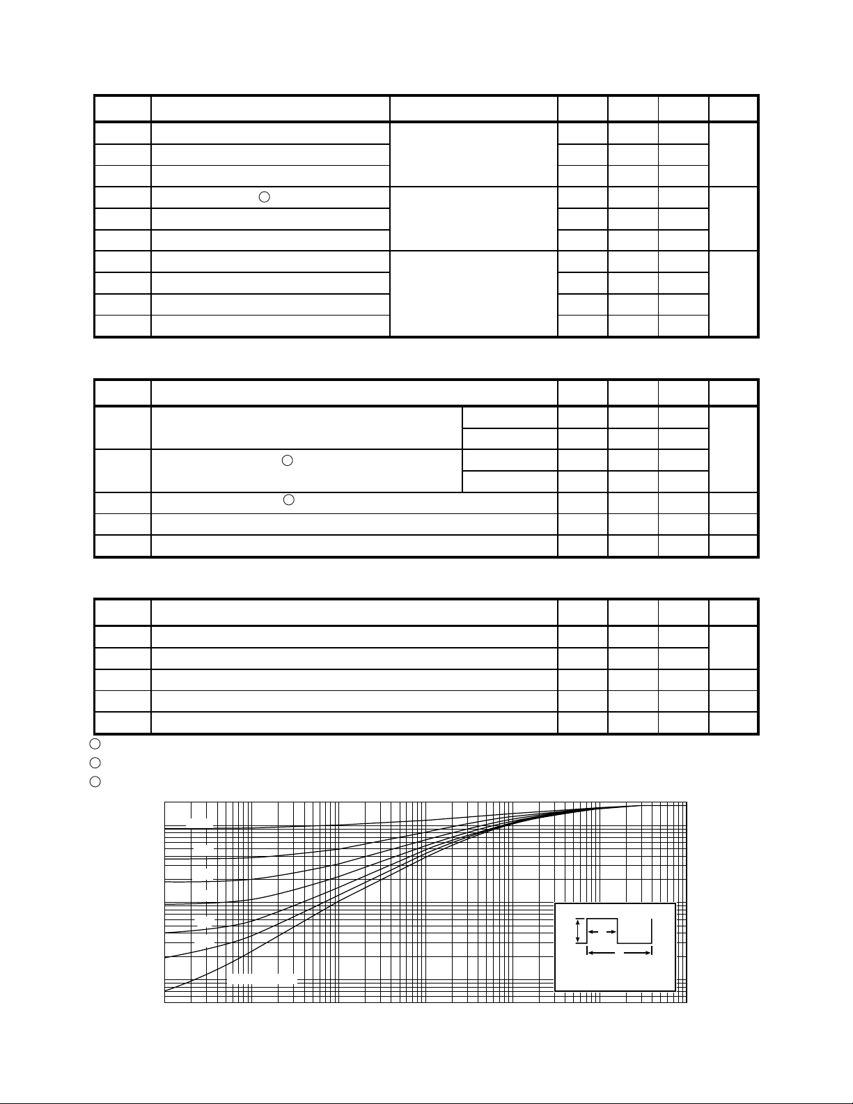
FIGURE 1, MAXIMUM EFFECTIVE TRANSIENT THERMAL IMPEDANCE, JUNCTION-TO-CASE vs PULSE DURATION
-4
10
-3
10
RECTANGULAR PULSE DURATION (SECONDS)
-2
10
MIN TYP MAX
2500
Note:
DM
P
Duty Factor D =
Peak TJ = PDM x Z
-1
10
1.0 10
Symbol
V
Isolation
C
Isolation
Torque
1
Repetitive Rating: Pulse width limited by maximum junction temperature. See Transient Thermal Impedance Curve. (Fig.1)
2
Pulse Test: Pulse width < 380 µS, Duty Cycle < 2%
3
See MIL-STD-750 Method 3471
050-8038 Rev E
UNIT
3
nH
5
Volts
70
13
t
1
t
2
t
1
/
t
2
+ T
θJC
C
pF
in-lbs
Page 3

APT8018JN
100
80
60
VGS=6, 8, 10 & 15V
5.5V
100
VGS=10 & 15V
8V
80
6V
5.5V
60
40
20
, DRAIN CURRENT (AMPERES)
D
4.5V
40
20
, DRAIN CURRENT (AMPERES)
D
4V
5V
0
0 100 200 300 400 0 5 10 15 20 25
VDS, DRAIN-TO-SOURCE VOLTAGE (VOLTS) VDS, DRAIN-TO-SOURCE VOLTAGE (VOLTS)
0
5V
4V
FIGURE 2, TYPICAL OUTPUT CHARACTERISTICS FIGURE 3, TYPICAL OUTPUT CHARACTERISTICS
100
TJ = -55°C
80
TJ = +25°C
TJ = +125°C
3.5
3.0
V
TJ = 25°C
250µSEC. PULSE TEST
@ <0.5 % DUTY CYCLE
NORMALIZED TO
= 10V @ 0.5 ID [Cont.]
GS
2.5
60
2.0
VGS=10V
40
TJ = +125°C
20
, DRAIN CURRENT (AMPERES) I
D
TJ = +25°C
0
0 2 4 6 8 10 0 40 80 120 160 200
V
, GATE-TO-SOURCE VOLTAGE (VOLTS) ID, DRAIN CURRENT (AMPERES)
GS
FIGURE 4, TYPICAL TRANSFER CHARACTERISTICS FIGURE 5, R
40
TJ = -55°C
VDS> ID (ON) x RDS (ON)MAX.
250µSEC. PULSE TEST
@ <0.5 % DUTY CYCLE
1.0
(ON), DRAIN-TO-SOURCE ON RESISTANCE I
DS
0.5
(ON) vs DRAIN CURRENT
DS
1.2
1.5
VGS=20V
4.5V
30
1.1
1.0
20
0.9
10
, DRAIN CURRENT (AMPERES) I
D
0
25 50 75 100 125 150 -50 -25 0 25 50 75 100 125 150
T
, CASE TEMPERATURE (°C) TJ, JUNCTION TEMPERATURE (°C)
FIGURE 6, MAXIMUM DRAIN CURRENT vs CASE TEMPERATURE FIGURE 7, BREAKDOWN VOLTAGE vs TEMPERATURE
2.5
C
ID = 0.5 ID [Cont.]
VGS = 10V
2.0
1.5
1.0
(NORMALIZED)
0.5
(ON), DRAIN-TO-SOURCE ON RESISTANCE I
0.0
DS
-50 -25 0 25 50 75 100 125 150 -50 -25 0 25 50 75 100 125 150
R
T
, JUNCTION TEMPERATURE (°C) TC, CASE TEMPERATURE (°C)
J
FIGURE 8, ON-RESISTANCE vs. TEMPERATURE FIGURE 9, THRESHOLD VOLTAGE vs TEMPERATURE
0.8
(ON), DRAIN-TO-SOURCE BREAKDOWN R
DSS
0.7
1.4
1.2
1.0
0.8
(NORMALIZED) VOLTAGE (NORMALIZED)
(TH), THRESHOLD VOLTAGE BV
0.6
GS
V
0.4
050-8038 Rev E
Page 4

200
100
OPERATION HERE
50
LIMITED BY R
(ON)
DS
10
5
1
TC =+25°C
.5
, DRAIN CURRENT (AMPERES)
D
TJ =+150°C
SINGLE PULSE
10µS
100µS
1mS
10mS
100mS
DC
50,000
10,000
5,000
1,000
500
APT8018JN
C
iss
C
oss
C
rss
.1
1 5 10 50 100 800 .1 .5 1 5 10 50
VDS, DRAIN-TO-SOURCE VOLTAGE (VOLTS) VDS, DRAIN-TO-SOURCE VOLTAGE (VOLTS)
100
FIGURE 10, MAXIMUM SAFE OPERATING AREA FIGURE 11, TYPICAL CAPACITANCE vs DRAIN-TO-SOURCE VOLTAGE
20
16
12
8
ID = ID [Cont.]
VDS=80V
VDS=160V
VDS=400V
400
100
T
=+150°C
J
T
=+25°C
J
50
T
=-55°C
10
J
5
4
, GATE-TO-SOURCE VOLTAGE (VOLTS) I
GS
V
0
0 200 400 600 800 1000 0 0.4 0.8 1.2 1.6 2.0
Q
, TOTAL GATE CHARGE (nC) VSD, SOURCE-TO-DRAIN VOLTAGE (VOLTS)
FIGURE 12, GATE CHARGES vs GATE-TO-SOURCE VOLTAGE FIGURE 13, TYPICAL SOURCE-DRAIN DIODE FORWARD VOLTAGE
g
, REVERSE DRAIN CURRENT (AMPERES) C, CAPACITANCE (pF)
DR
1
I
APT Reserves the right to change, without notice, the specifications and information contained herein.
SOT-227 (ISOTOP®) Package Outline
11.8 (.463)
12.2 (.480)
31.5 (1.240)
31.7 (1.248)
7.8 (.307)
8.2 (.322)
W=4.1 (.161)
W=4.3 (.169)
H=4.8 (.187)
H=4.9 (.193)
(4 places)
8.9 (.350)
9.6 (.378)
Hex Nut M4
(4 places)
®
ISOTOP
050-8038 Rev E
r = 4.0 (.157)
(2 places)
is a Registered Trademark of SGS Thomson.
14.9 (.587)
15.1 (.594)
30.1 (1.185)
30.3 (1.193)
38.0 (1.496)
38.2 (1.504)
4.0 (.157)
4.2 (.165)
(2 places)
3.3 (.129)
3.6 (.143)
* Source Drain
* Source
Dimensions in Millimeters and (Inches)
0.75 (.030)
0.85 (.033)
1.95 (.077)
2.14 (.084)
25.2 (0.992)
12.6 (.496)
12.8 (.504)
*
Source terminals are shorted
internally. Current handling
capability is equal for either
Source terminal.
25.4 (1.000)
Gate
 Loading...