

Page 1
Copyright ANPEC Electronics Corp.
Rev. A.6 - Dec., 2001
APT7846
www.anpec.com.tw1
ANPEC reserves the right to make changes to improve reliability or manufacturability without notice, and advise
customers to obtain the latest version of relevant information to verify before placing orders.
Touch Screen Controller
Description
The APT7846 is enhance function of APT7843 added
battery and temperature monitor function and offer
of a bandgap reference voltage for system user. The
APT7846 Touch Screen Controller IC provides all the
screen driver , A/D converter and control circuits to
easily interface to 4 wire resistive touch screen.
The IC continually monitors the screen waiting for a
touch. When the screen touched , the IC performs
A/D converter to determine the location of touch.
Also , this device has 1 auxiliary input to A/D converter , allowing for the measurement of other input
signal.
Applications
••
••
• PDAs
••
••
• Hand held computer
••
••
• Touch-screen mobile phone
••
••
• Protable electronic dictionary
••
••
• Smart IA
Features
••
••
•
16 Pin SSOP or TSSOP
••
••
•
Operates With Four Wire Touch Screen
••
••
•
8-Bit or 12-Bit A/D Converter
••
••
•
Ratiometric Conversion Eliminates Screen
Calibration
••
••
•
1 Auxiliary Analog Input
••
••
• Full Power Down Control
••
••
• Internal Bandgap Reference
••
••
• Serial Interface To Microprocessor
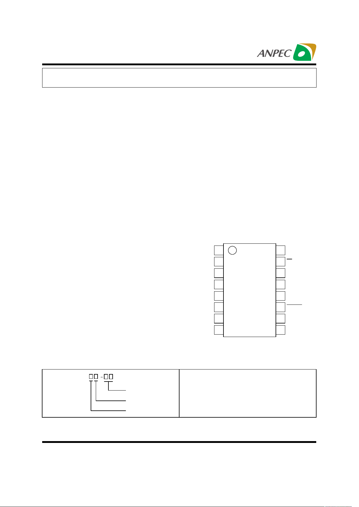
Pin Assignment
Ordering Information
+Vcc 1
14
15
16
8
7
6
5
4
3
2
11
12
13
9
10V
*)6
GND
Y-
X-
Y+
X+
DOUT
BUSY
DIN
DCLK
IN V
4-.
+Vcc
CS
PENIRQ
APT7846
Temp. Range
Package Code
Package Code
N : SSOP O : TSSOP
Temp. Range
I : - 40 to 85 C
Handling Code
TU : Tube TR : Tape & Reel
°
Handling Code
Page 2
Copyright ANPEC Electronics Corp.
Rev. A.6 - Dec., 2001
APT7846
www.anpec.com.tw2
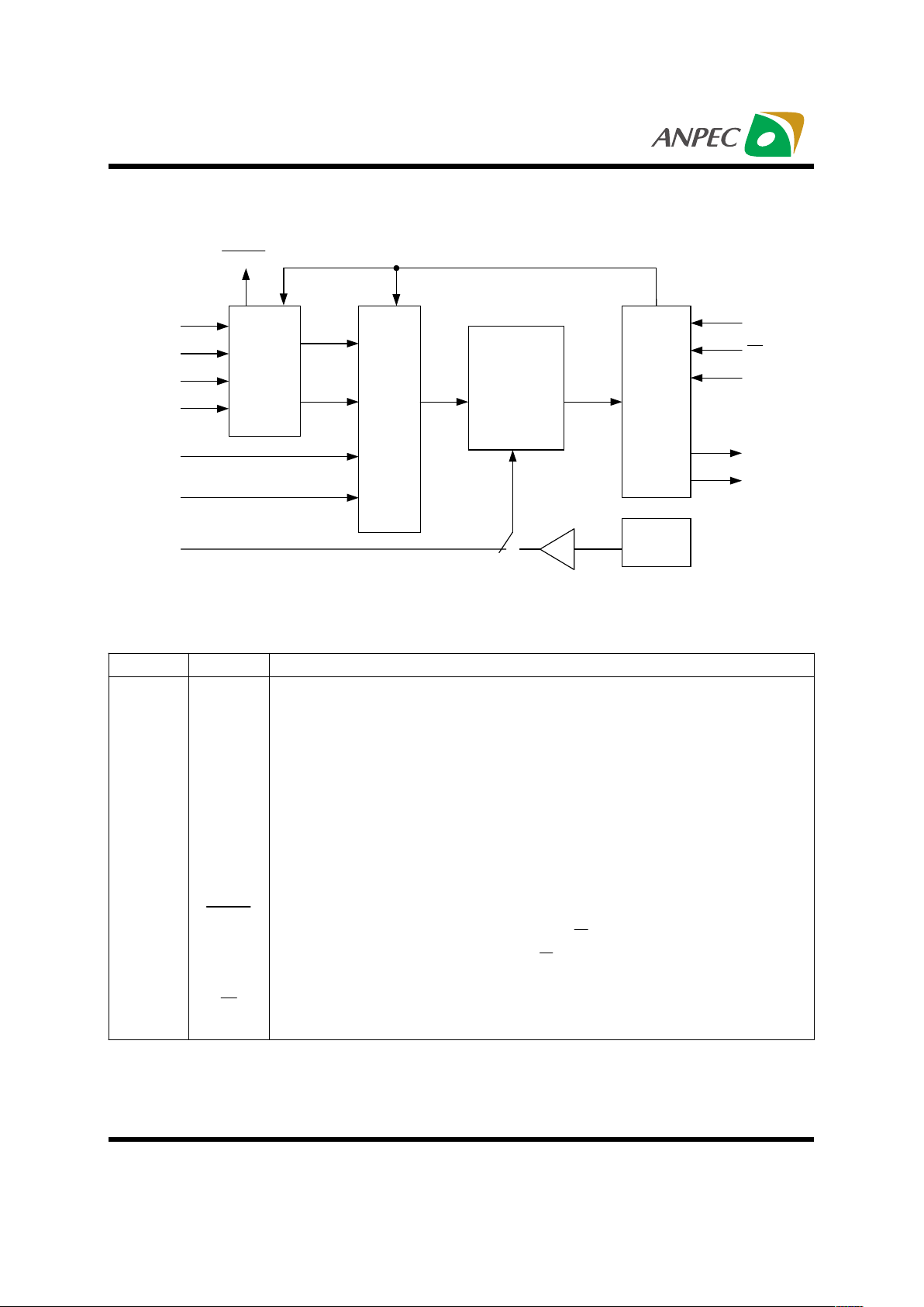
Pin Description
Block Diagram
PIN NAME
DESCRIPTION
1+Vcc
Power Supply , 2.7V to 5V.
2X+
Connect to X+ on touch screen.
3Y+
Connect to Y+ on touch screen.
4X-
Connect to X- on touch screen.
5Y-
Connect to Y- on touch screen.
6GND
Ground
7V
*)6
Measure Battery Input.
8IN
Auxiliary input of A/D converter.
9V
4-.
Voltage Reference Input or Output.
10 +Vcc Power Supply , 2.7V to 5V.
11 PENIRQ Pen interrupt. (requires to 100kΩ pull-up resistor externally)
12 DOUT Serial Data Output. This output is high impedance when CS is HIGH.
13 BUSY Busy Output. This output is high impedance whenCS is HIGH.
14 DIN Serial Data input.
15 CS Chip Select. (Active Low)
16 DCLK Serial Clock.
V4-.
IN
V
*)6
Y-
Y+
X+
X-
PENIRQ
DOUT
BUSY
CS
DIN
DCLK
12 Bit or 8 Bit
A/D Converter
Serial
Interface
Screen Driver
MUX
Internal
Reference
Page 3
Copyright ANPEC Electronics Corp.
Rev. A.6 - Dec., 2001
APT7846
www.anpec.com.tw3
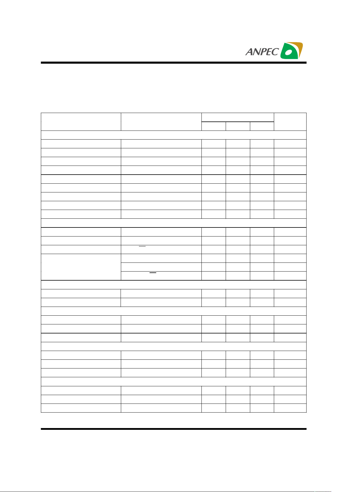
Electrical Characteristics
At TA = -40°C to 85°C, V
CC
= +2.7V , V
REF
= +2.5V , f
SAMPLE
= 125kHz , f
CLK
= 16 f
SAMPLE
= 2MHz , 12-bit mode
, and digital inputs = GND or Vcc , unless otherwise noted.
APT7846
PARAMETER CONDITIONS
MIN TYP MAX
UNIT
DC ACCURACY
Resolution 12 Bits
No missing code 11 Bits
Integral Nonlinearity
±
2 LSB
Offset Error
±
6 LSB
Offset Error Match 0.1 1 LSB
Gain Error
±
4 LSB
Gain Error Match 0.1 1 LSB
Noise 30 uV rms
Power Supply Rejection 70 dB
REFERENCE INPUT
V
REF
Input Voltage Range 1.0 Vcc
DC Leakage Current
±
1
µ
A
V
REF
Input Impedance CS = GND or Vcc 5
G
Ω
V
REF
Input Current 13 40
µ
A
F
SAMPLE
= 12.5 kHz 2.5
µ
A
CS = Vcc 3
µ
A
REFERENCE OUTPUT
Internal Reference Voltage 2.4 2.5 2.6 V
Input Impedence Internal Reference Off 1
G
Ω
DYNAMIC PERFORMANCE
Aperture Delay 30 ns
Aperture Jitter 100 ps
Channel to Channel Isolation VIN = 2.5Vp-p ; FIN = 50kHz 100 dB
CONVERSION RATE
Conversion Time 12 DCLK cycles
Track/Hold Acquisition Time 3 DCLK cycles
Throughput Rate 125 KSPS
SWITCH DRIVERS
On-Resistance
Y+ , X+ 4 15
Ω
Y- , X- 4 15
Ω
Page 4
Copyright ANPEC Electronics Corp.
Rev. A.6 - Dec., 2001
APT7846
www.anpec.com.tw4
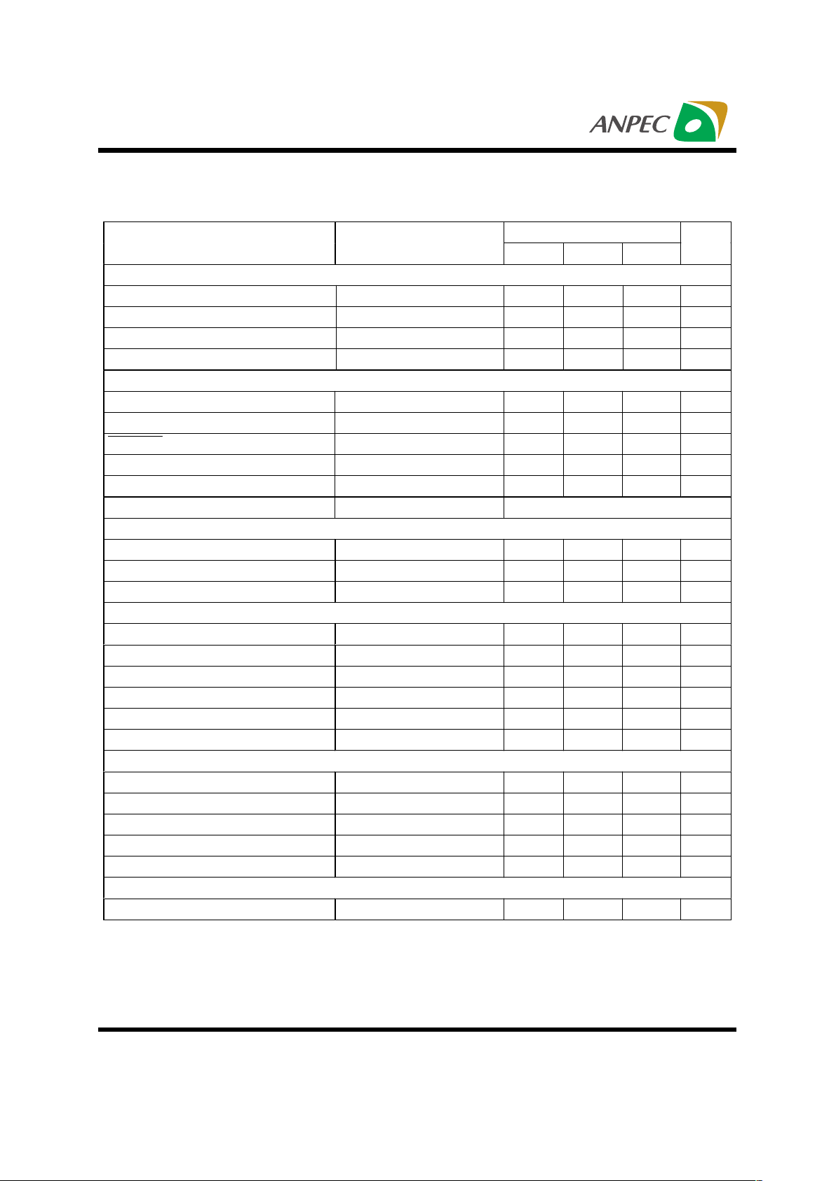
Electrical Characteristics (Cont.)
Note : (1) LSB means least Significant Bit. With V
REF
equal to +2.5V , one LSB is 610µV
APT7846
PARAMETER CONDITIONS
MIN TYP MAX
UNIT
LOGIC INPUTS
Input High Voltage , V
INH
|I
INH
| ≤ +5µA2.4 V
Input Low Voltage , V
INL
|I
INL
| ≤ +5µA0.8V
Input Current , I
IN
±
1
µ
A
Input Capacitance , C
IN
10 pF
LOGIC OUTPUTS
Output High Voltage , V
OH
|IOH| ≤ -250µA
Vcc0. 2
V
Output Low Voltage , V
OL
|IOL| ≤ 250µA0.4V
PENIRQ output low voltage , V
OL
0.2 V
Floating-State Leakage Current
±
10
µ
A
Floating-State Output Capacitance 10 pF
Output Coding Straight ( Natural ) Binary
ANALOG INPUT
Input Voltage Ranges 0 V
REF
V
DC Leakage Current
±
0.1
µ
A
Input Capacitance 30 pF
POWER REQUIREMENTS
Vcc 2.7 3.6 V
Icc Digital I/Ps =0V or Vcc
Normal Mode (Static) Vcc = 3.6V 650
µ
A
Normal Mode (F
SAMPLE
= 12.5kSPS) Vcc = 3.6V 540
µ
A
Shutdown Mode(Static) 3
µ
A
Showdown Vcc = 3.6V 3.6
µ
W
BATTERY MEASURE
Input Voltage Range 0.5 6 V
Input impedance
Sample Battery On 10 K
Ω
Sample Battery Off 1 G
Ω
Accuracy V
REF
-2 2 %
TEMPERATURE RANGE
Normal Operation -40 85
°
C
Page 5
Copyright ANPEC Electronics Corp.
Rev. A.6 - Dec., 2001
APT7846
www.anpec.com.tw5
FIGURE 1. Basic Operation of the APT7846
Chip Overview
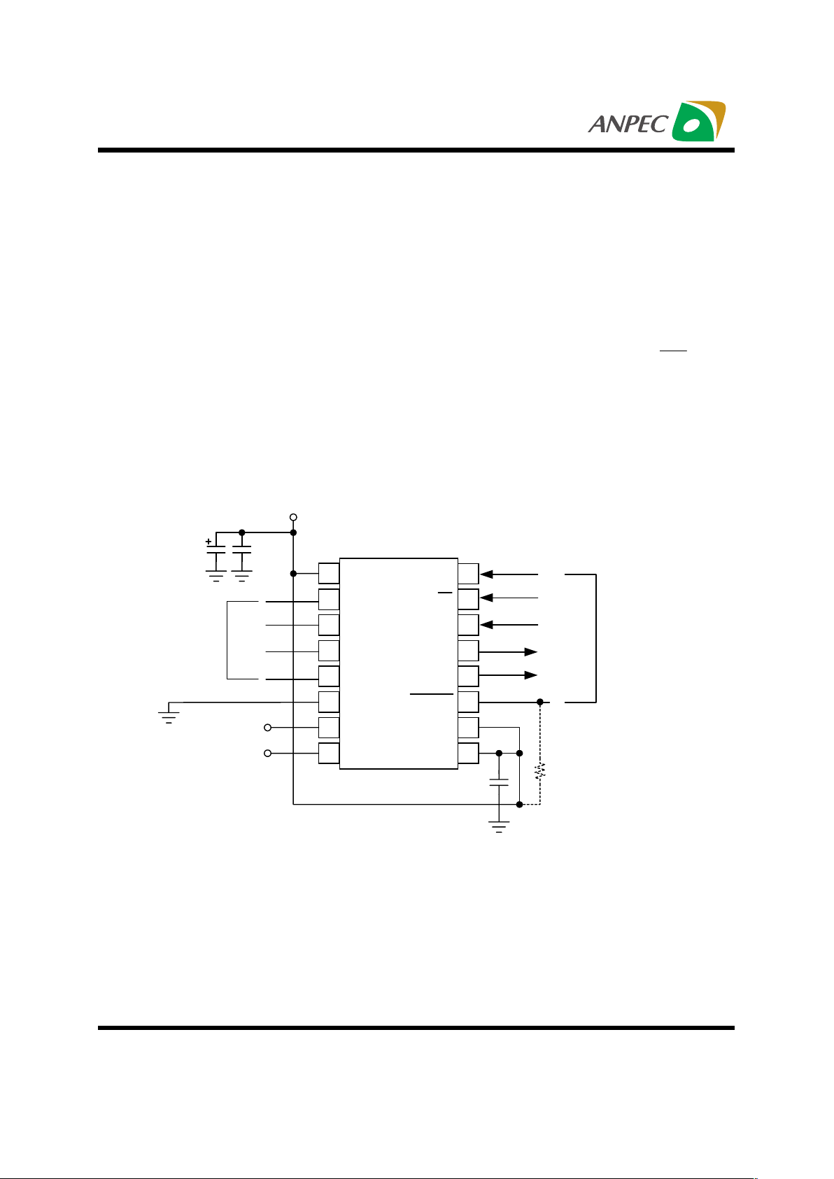
The APT7846 is a successive approximation analog-to-digital (A/D) converter based around a capacitive redistribution DAC. Figure 1 show basic operation of the APT7846.
The APT7846 communicates via a 4-wire serial
interface. The device requires an external reference voltage Vref. The value of the reference voltage directly sets the input range of the converter.
Otherwise you can use internal reference Voltage to
do conversion.
The APT7846 primary function is to control resistive
touchscreens. When a touch is detected , pen interrupt pin will go low to wake up extenal microprocessor . The microprocessor writes register to initiate
Analog Input
The analog input to the converter is provided via a
four-channel multiplexer. Figure 2 shows a simplified diagram of the APT7846 with the difference input of the A/D converter , and the converters
reference. Table I and Table II also show the relationship between the A2 , A1 , A0 , SER/ and the
configuration of the APT7846. See the section of
single-ended reference mode and differential reference mode for more details.
,.4
conversion.
This A/D converter may also be used to measure
voltage presented on the IN Pin or to measure battery presented on the V
BAT
Pin.
1
14
15
16
8
7
6
5
4
3
2
11
12
13
9
10
V
BAT
GND
Y-
X-
Y+
X+
DOUT
BUSY
DIN
DCLK
IN V
REF
+Vcc
CS
PENIRQ
+Vcc
APT7846
100k ohm (optional)
Auxiliary Input
+2.7V to +5v
To
Touch
Screen
1uF
to
10uF
(Optional)
0.1uF
0.1uF
Connect to
Microprossor
Battery Input
Page 6

Copyright ANPEC Electronics Corp.
Rev. A.6 - Dec., 2001
APT7846
www.anpec.com.tw6
A2 A1 A0 +REF -REF Y- X+ Y+ Y-POSITION X-POSITION Z1-POSITION Z2-POSITION DRIVERS ON
0 0 1 Y+ Y- +IN Measure Y+,Y0 1 1 Y+ X- +IN Measure Y+,X-
1 0 0 Y+ X- +IN Measure Y+,X-
1 0 1 X+ X- +IN Measure X+,X-
TABLE I. Input Configuration , Single-Ended Reference Mode (SER/
,.4
HIGH).
TABLE II. Input Configuration , Differential Reference Mode (SER/
,.4
LOW).
FIGURE 2. Simplified Diagram of Analog Input
A2 A1 A0 V
BAT
AUXINTEMP Y- X+ Y+ Y-POSITION
X-
POSITION
Z
1
-
POSITION
Z2-
POSITIONX-DRIVERSY-DRIVERS
000
+IN(TEMP 0)
OFF OFF
001 +IN Measure OFF ON
010+IN OFF OFF
0 1 1 +IN Measure X-,ON Y+,ON
1 0 0 +IN Measure X-,ON Y+,ON
1 0 1 +IN Measure ON OFF
110 +IN OFF OFF
111
+IN(TEMP 1)
OFF OFF
X+
X-
Y+
Y-
V
BAT
IN
GND
+Vcc
A2-A0
(Shown 001
B
)
SER/DFR
(Shown HIGH)
PENIRQ
V
REF
7.5K
Ω
2.5K
Ω
Battery
On
+IN
-IN
+REF
CONVERTER
-REF
2.65V
Reference
Ref ON/OFF
TEMP 0TEMP 1
Page 7

Copyright ANPEC Electronics Corp.
Rev. A.6 - Dec., 2001
APT7846
www.anpec.com.tw7
Single-Ended reference mode
Figure 3 shows the diagram of single-ended reference mode.
This application shows the measurement of current
Y poisition is made by connecting the X+ input to the
A/D converter , turning on the Y+ and Y- drivers , and
digitizing the voltage on X+. For this measurement ,
the resistance in the X+ lead does not affect the
conversion. However , since the resistance between
Y+ and Y- is fairly low , the on-resistance of the Y
drivers does make a small difference. Under the situation outlined so far , it would not be possible to
achieve a zero volt input or a full-scale input regardless of where the pointing device is on the touch
screen because some voltage is lost across the internal switches. This situation can be remedied if
use differential reference mode
GND
Y+
X+
Y-
+Vcc
V
REF
+IN
-IN
Converter
+REF
-REF
Y Switch ON
GND
FIGURE 3. Single-Ended Reference Mode
(SER/ High , A2=Low , A1=Low , A0=High)
As shown in Figure 4 , by setting the SER/ bit
LOW , the +REF and -REF inputs are connected directly to Y+ and Y-. This makes the analog-to-digital
conversion ratiometric.
The result of the conversiong is always a percentage
of the external resistance , reardless of how it changes
in relation to the on-resistance of the internal switches.
Note that there is an important consideration regarding power dissipation when using the ratiometric mode
of operation , the external device should powered
throughout the acquisition and conversion periods.
Differential reference mode
Figure 4. Differential Reference Mode
(SER/ LOW , A2=Low , A1=Low , A0=High)
Data is written to , and read from , the APT7846 via
the serial port. The serial port has 4 pins - serial
clock (DCLK) , chip select ( ) , data in (DIN) and
data out (DOUT). The DCLK acts on the rising edge.
The acts as a reset for the serial port with goes
low initiating a conversion cycle. The cycle consists
of 2 parts - a write followed by a read. Figure 5 shows
the typical timing of the APT7846s serial interface.
A total of 24 clock cycles will complete one
conversion.
Also shown in Figure 5 is the placement and order of
the control bits within the control byte. Tables III and
IV give detailed information about these bits.
The first bit , the ′S′ bit , must always be HIGH and
indicates the start of the control byte. The APT7846
will ignore inputs on the DIN pin until the start bit S
detected.
The next three bits (A2 - A0) select the active input
channel or channels of the input multiplexer (see
Tables I and II and Figure 2).
The MODE bit determines the number of bits for each
conversion , either 12 bits (LOW) or 8 bits (HIGH).
The SER/ bit controls the reference mode: either
single-ended (HIGH) or differential (LOW). (The differential mode is also referred to as the ratiometric
conversion mode.)
The last two bits (PD1 - PD0) select the power- down
mode as shown in Table V. If both inputs are HIGH
, the device is always powered up. If both inputs are
LOW , the device enters a power-down mode between conversions.
Serial Interface
CS
,.4
CS
,.4
+5
,.4
GND
Y+
X+
Y-
+Vcc
Y+
+IN
-IN
Converter
+REF
-REF
Y Switch ON
Y-
,.4
Page 8

Copyright ANPEC Electronics Corp.
Rev. A.6 - Dec., 2001
APT7846
www.anpec.com.tw8
PD1 PD0 PENIRQ DESCRIPTION
0 0 Enabled
Power-down between conversions. When
each conversion is finished, the converter
enters a low power mode.
0 1 Enabled Reference is OFF.
1 0 Enabled Reference is ON
1 1 Disabled
No power-down between conversions,
device is always powered.
DCLK
CS
DOUT
BUSY
DIN
t
ACQ
ldle Acquire Conversion ldle
(MSB) (LSB)
11 10 9 8 7 6 5 4 3 2 1 0
(START)
S
A2 A1 A0
2, 2,
SER/
DFR
MODE
1818 81
FIGURE 5. Conversion Timing , 24-Clocks per Conversion , 8-bit Bus Interface. No DCLK Delay Required
with Dedicated Serial Port.
BIT NAME DESCRIPTION
7 S Start Bit. Control byte starts with first HIGH bit on
DIN. A new control byte can start every 15th clock
cycle in 12-bit conversion mode or every 11th clock
cycle in 8-bit conversio n mode.
6-4 A2-A0 Channel Select Bits. Along with the SER/DFR bit,
these bits control the setting of the multiplexer
input, switches, and reference inputs, as detailed in
Tables I and II.
3 MODE 12-Bit/8-Bit Conversion Select Bit. This bit controls
the number of bits for the following conversion: 12bits(LOW) or 8-bits(HIGH).
2 SER/DFR Single-Ended/Differential Reference Select Bit.
Along with bits A2-A0, this bit controls the setting of
the multiplexer input, switches, and reference
inputs, as detailed in Tables I and II.
1-0 PD1-PD0 Power-Down Mode Select Bits. See Table V for
details.
TABLE III. Order of the Control Bits in the Control
Byte.
TABLE IV. Descriptions of the Control Bits within the
Control Byte.
Bit 7 Bit 6 Bit 5 Bit 4 Bit 3 Bit 2 Bit 1 Bit 0
(MSB) (LSB)
S A2A1A0MODESER/DFRPD1PD0
TABLE V. Power-Down Selection.
Page 9

Copyright ANPEC Electronics Corp.
Rev. A.6 - Dec., 2001
APT7846
www.anpec.com.tw9
TEMPERATURE MEASUREMENT
The temperature measurement technique used in the
APT7846 relies on the characteristics of a semiconductor junction operation at a fixed current level. The
forward bipolar transistor voltage (V
BE ) has a well
defined characteristic versus temperature.
If you got 25°C value of the VBE voltage then measured ambient temperature to monitor the voltage
variance.
There are two mode to measure temperature. The
Temp 0 requires calibration at a known temperature
, but only requires a single reading to predict the ambient temperature. The PENIRQ bipolar transistor is
used during this measurement , the A/D with an address of A2=0 , A1=0 and A0=0 (see Table I and
Figure 6). This voltage is typically 600mV at +25°C ,
with a 20µA current through it. The TC of temperature Temp 0 is very consistent at 2.1 mV/°C. Catch
the bipolar transistor voltage on room temperature ,
in memory , for calibration purposes by the user.
The Temp 1 requires two steps to measure
temperature.
First step read Temp 0 voltage. Second step read
address of A2=1 , A1=1 , and A0=1 , with an 82 times
large current.
The voltage difference between the Temp 0 and
Temp 1 conversion using 82 times the bias.
FIGURE 6. Functional Block Diagram of Temperature Measurement Mode..1/URE
MUX
A/D
Converter
Current will be represented by kT/q ∗ ln (N) , where N
is the current ratio = 82 , k = Boltzmanns constant
(1.38054 ∗ 10e23 electrons volts/degrees Kelvin) ,
q = the electron charge (1.602189 ∗ 10e19 C) , and
T = the temperature in degrees Kelvin. The resultant
equation for solving for °K is :
°K = q ∗ ∆V / ( k ∗ In ( N ) ) (1)
where , ∆V = V( Ι
82 ) V ( Ι1 ) ( mV )
∴ °K = 2.30 ∆V ( °K / mV )
°C = 2.30 ∆V ( mV ) 273 °K
BATTERY MEASUREMENT
An added feature of the APT7846 is the ability to
monitor the battery voltage , as shown in Figure7.
The battery voltage can vary from 0.5V to 6V , while
maintaining the voltage to the APT7846 at 2.7V ,
3.3V , etc. The input voltage (V
BAT
) is divided down
by 4 so that a 6.0V battery voltage is represented as
1.5V to the ADC. This simplifies the multiplexer and
control logic. In order to minimize the power consumption , the divider is only ON during the samling
of DIN to A2=0 , A1=1 , and A0=0. Tables I and II
show the relationship between the control bits and
configuration of the APT7846.
DC/DC
Converter
Vcc
0.125V to 1.5V
V
BAT
7.5k
Ω
2.5k
Ω
Battery
0.5V
to
6.0V
FIGURE 7. Battery Measurement Functional Block
Diagram.
Page 10

Copyright ANPEC Electronics Corp.
Rev. A.6 - Dec., 2001
APT7846
www.anpec.com.tw10
There are total of four measurements possible :
Calculating Touch Resistance
MEASURE DRIVE PIN MEASURED RESULT
X-position X+,X- Y+ A
Y-position Y+,Y- X+ B
Z1-position Y+,X- X+ C
Z2-position Y+,X- Y- D
The APT7846 has an internal 2.5V voltage reference
that can be turned ON and OFF with the power-down
address PD1=1(see table V). Typically , the internal
reference voltage is only used in the single-ended
mode for battery monitoring , temperature measurement , and for utilizing the auxiliary input. Optimal
Internal Reference
touch-screen performance is achieved when utilizing the differential mode. The internal reference voltage of the APT7846 must be commanded to be off to
maintain compatibility with the APT7843. Therefore ,
after power-up , a write of PD1=0 is required to insure the reference is off.
FIGURE 8 is Pressure measurement diagram.
X+ Y+
X- Y-
Touch
Measure Z 2-Position
Z2-Position
X+ Y+
X- Y-
Touch
Measure Z 1-Position
Z1-Position
X+ Y+
X- Y-
Touch
Measure X -Position
X-Position
FIGURE 8 is Pressure measurement diagram.
where the result is a number from 0 to 4096.
From simple network theory , RTHOUCH can be represented in many ways , 2 are given below :
or
R
THOUGH
=
R
X
C
*
A
4096
*
( 4096 - C )
- R
Y
+ R
Y
*
B
4096
R
THOUGH
= R
X
A
4096
**
D
C
-1 )
(
where RY = Y plate resistance
where R
X
= X plate resistance
Page 11

Copyright ANPEC Electronics Corp.
Rev. A.6 - Dec., 2001
APT7846
www.anpec.com.tw11
The APT7846 will alow a conversion every 16 clock
cycles , as shown in Figure 10. This figure shows
possible serial communication occurring with other
serial peripherals between each byte transfer between the processor and the converter.
Figure 11 provides the fastest way to clock the
APT7846. This method will not work with the serial
interface of most microcontrollers and digital signal
processors as they are generally not capable of providing 15 clock cycles per serial transfer. However ,
16-Clocks or 15-Clocks per Conversion
AC Timing
The pen interrupt output function is detailed in Figure
9. By connecting a pull-up resistor to VCC (typically
100kΩ) , the output is HIGH. While in the
power-down mode , with PD0 = PD1 = 0 , the Y
driver is ON and connected to GND and the .
output is connected to the X+ input. When the panel
is touched , the X+ input is pulled to ground through
the touch screen and output goes LOW due
to the current path through the panel to GND , initiating an interrupt to the processor. During the measurement cycles for X- and Y-Position , the
output diode will be internally connected to GND and
the X+ input disconnected from the diode to
eliminate any leakage current from the pull-up resistor to flow through the touch screen , thus causing no
errors.
PENIR
Q
PENIRQ
PENIRQ
PENIRQ
PENIRQ Output
PENIRQ
SYMBOL DESCRIPTION MIN TYP MAX UNIT
t
ACQ
Acquisition Time 1.5
µ
s
t
DS
DIN Valid Prior to DCLK Rising 100 ns
t
DH
DIN Hold After DCLK HIGH 10 ns
t
DO
DCLK Falling to DOUT Vaild 200 ns
t
DV
CS Falling to DOUT Enabled 200 ns
t
TR
CS Rising to DOUT Disabled 200 ns
t
CSS
CS Falling to DC LK Rising 100 ns
t
CSH
CS Rising to DCLK lgnored 0 ns
t
CH
DCLK HIGH 200 ns
t
CL
DCLK LOW 200 ns
t
BD
DCLK Falling to BUSY Rising 200 ns
t
BDV
CS Falling to BUSY Enabled 200 ns
t
BTR
CS Rising to BUSY Disable 200 ns
Figure 12 and Table VI provide detailed timing of
the APT7846.
TABLE VI. Timing Specifications (+Vcc=+2.7V and
Above , TA=-40°C to +85°C , CLOAD=50pF).
this method could be used with field programmable
gate arrays (FPGAs) or application specific integrated
circuits (ASICs). (Note that this effectively increases
the maximum conversion rate of the converter).
FIGURE 9. PERIRQ Functional Block Diagram
+Vcc
Y+
X+
Y-
ON
Y+,Y- Driver
100k
Ω
PENORQ
Page 12

Copyright ANPEC Electronics Corp.
Rev. A.6 - Dec., 2001
APT7846
www.anpec.com.tw12
FIGURE 11. Maximum Conversion Rate , 15-Clocks per Conversion.
DCLK
CS
DOUT
BUSY
DIN
1 11515 1
SS
S
11
10 9 7 6 5 01
2
34
11 10 9
886
75432
) ) )
2, 2,
MODE
SGL/
DIF
) )
2, 2,
MODE
SGL/
DIF
) )) )
DCLK
CS
DOUT
BUSY
DIN
CONTROL BITS
1 81 81 81
SS
CONTROL BITS
11 1098765
012
34
11 10
9
FIGURE 10. Conversion Timing , 16-Clocks per Conversion , 8-bit Bus Interface. No DCLK Delay Required with Dedicated Serial Port.
Page 13

Copyright ANPEC Electronics Corp.
Rev. A.6 - Dec., 2001
APT7846
www.anpec.com.tw13
DCLK
CS
DOUT
BUSY
DIN
t
CSS
t
CH
t
CL
t
DH
t
DS
t
BD
t
BD
t
BD
t
CSH
t
BTR
t
TR
t
BDV
t
DV
11 10
2,
FIGURE 12. Detailed Timing Diagram.
Anpec Electronics Corp.
Head Office :
5F, No. 2 Li-Hsin Road, SBIP,
Hsin-Chu, Taiwan, R.O.C.
Tel : 886-3-5642000
Fax : 886-3-5642050
Taipei Branch :
7F, No. 137, Lane 235, Pac Chiao Rd.,
Hsin Tien City, Taipei Hsien, Taiwan, R. O. C.
Tel : 886-2-89191368
Fax : 886-2-89191369
Customer Service
Page 14

Copyright ANPEC Electronics Corp.
Rev. A.6 - Dec., 2001
APT7846
www.anpec.com.tw14
Packaging Information
N
12
3
EH
D
L
GAUGE
PLANE
1
e
B
A1
A
Millimeters Variations- D Inches Variations- D
Dim
Min. Max. Variations Min. Max.
Dim
Min. Max. Variations Min. Max.
A1.350
1.75
SSOP-16
4.75 5.05
A 0.053 0.069 SSOP-16 0.187 0.199
A1
0.10 0.25
A1 0.004 0.010
B
0.20 0.30
B 0.008 0.012
D See variations D See variations
E
3.75 4.05
E 0.147 0.160
e 0.625 TYP. e 0.025 TYP.
H
5.75 6.25
H 0.226 0.246
L
0.4 1.27
L 0.016 0.050
N See variations N See variations
φ
1 0
°
8
°φ
1 0
°
8
°
SSOP
Page 15

Copyright ANPEC Electronics Corp.
Rev. A.6 - Dec., 2001
APT7846
www.anpec.com.tw15
Packaging Information
L
(3)
(2)
0.25
GAUGE
PLANE
1
b
A1
A2
A
D
e
2 x E / 2
E1 E
e/2
N
12
3
Millimeters Inches
Dim
Min. Max. Min. Max.
A 1.2 0.047
A1 0.00 0.15 0.000 0.006
A2 0.80 1.05 0.031 0.041
b 0.19 0.30 0.007 0.011
D
4.9 (N=16PIN)
6.4 (N=20PIN)
7.7 (N=24PIN)
9.6 (N=28PIN)
5.1 (N=16PIN)
6.6 (N=20PIN)
7.9 (N=24PIN)
9.8 (N=28PIN)
0.193 (N=16PIN)
0.252 (N=20PIN)
0.303 (N=24PIN)
0.378 (N=28PIN)
0.201 (N=16PIN)
0.260 (N=20PIN)
0.311 (N=24PIN)
0.386 (N=28PIN)
e 0.65 BSC 0.026 BSC
E
6.40 BSC 0.252 BSC
E1
4.30 4.50 0.169 0.177
L 0.45 0.75 0.018 0.030
φ
10
°
8
°
0
°
8
°
φ
212
°
REF 12° REF
φ
312
°
REF 12° REF
TSSOP
 Loading...