

Page 1
APT7843
Touch Screen Controller
Description
The APT7843 Touch Screen Controller IC provides all
the screen drive , A/D converter and control circuits
to easily interface to 4 wire resistive touch screen.
The IC continually monitors the screen waiting for a
touch. When the screen touched , the IC performs
A/D converter to determine the location of touch.
Also , this device has 2 auxiliary input to A/D converter , allowing for the measurement of other inputs
such as battery voltage.
Applications
•
PDAs
• Handheld computer
• Touch-screen kiosks
Features
•
16 pin SSOP or TSSOP
• Operates with four wire touch screen
• 8-bit or 12 bit A/D converter
• Ratiometric Conversion eliminates screen
calibration
• 2 auxiliary analog inputs
• 4 wire serial interface
• Full power down control
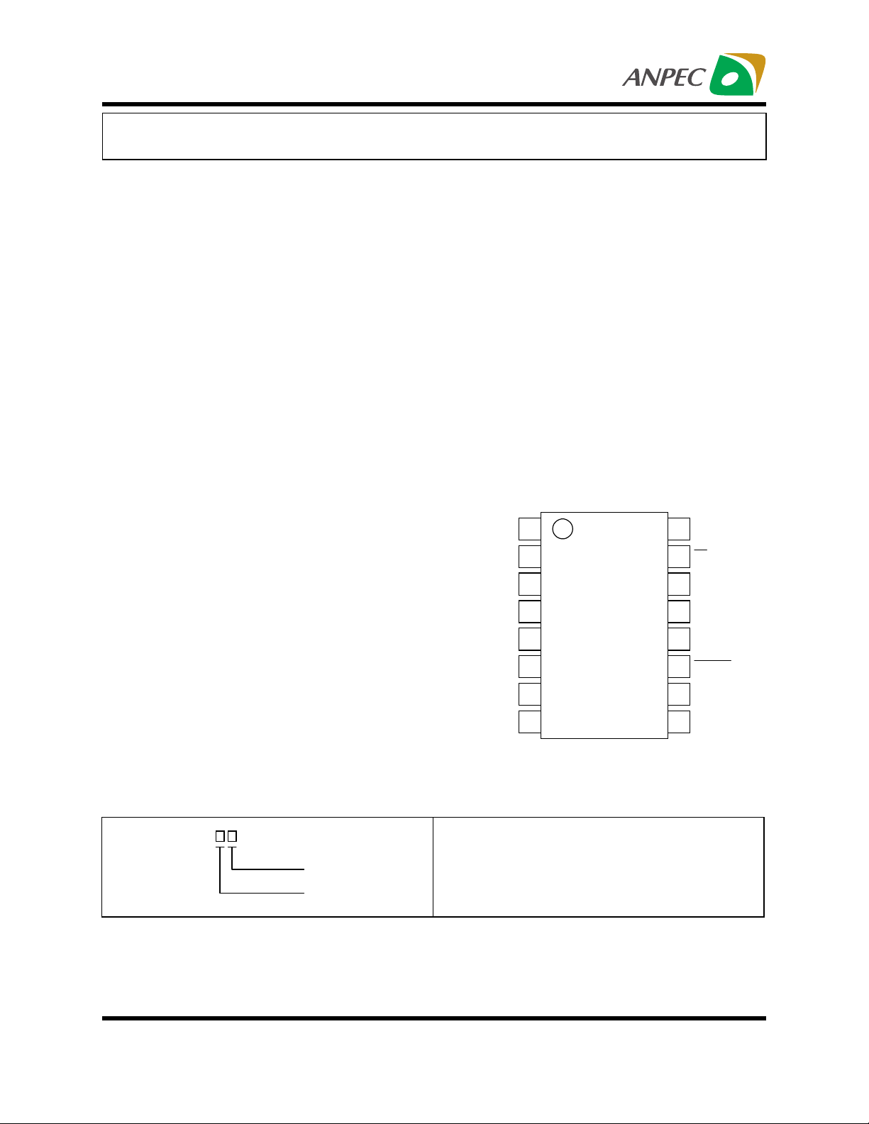
Pin Assignment
+Vcc 1
X+
Y+
2
3
DCLK
16
15
CS
14
DIN
4
X-
5
Y-
6
GND
7
IN4 V
8
13
12
11
10IN3
9
BUSY
DOUT
PENIRQ
+Vcc
REF
Order Information
APT7843
Temp. Range
Package Code
ANPEC reserves the right to make changes to improve reliability or manufacturability without notice, and advise
customers to obtain the latest version of relevant information to verify before placing orders.
Package Code
N : SSOP O : TSSOP
Temp. Range
I : - 40 to 85 C
°
Copyright ANPEC Electronics Corp.
Rev. A.8 - Apr., 2002
www.anpec.com.tw1
Page 2
APT7843
y)
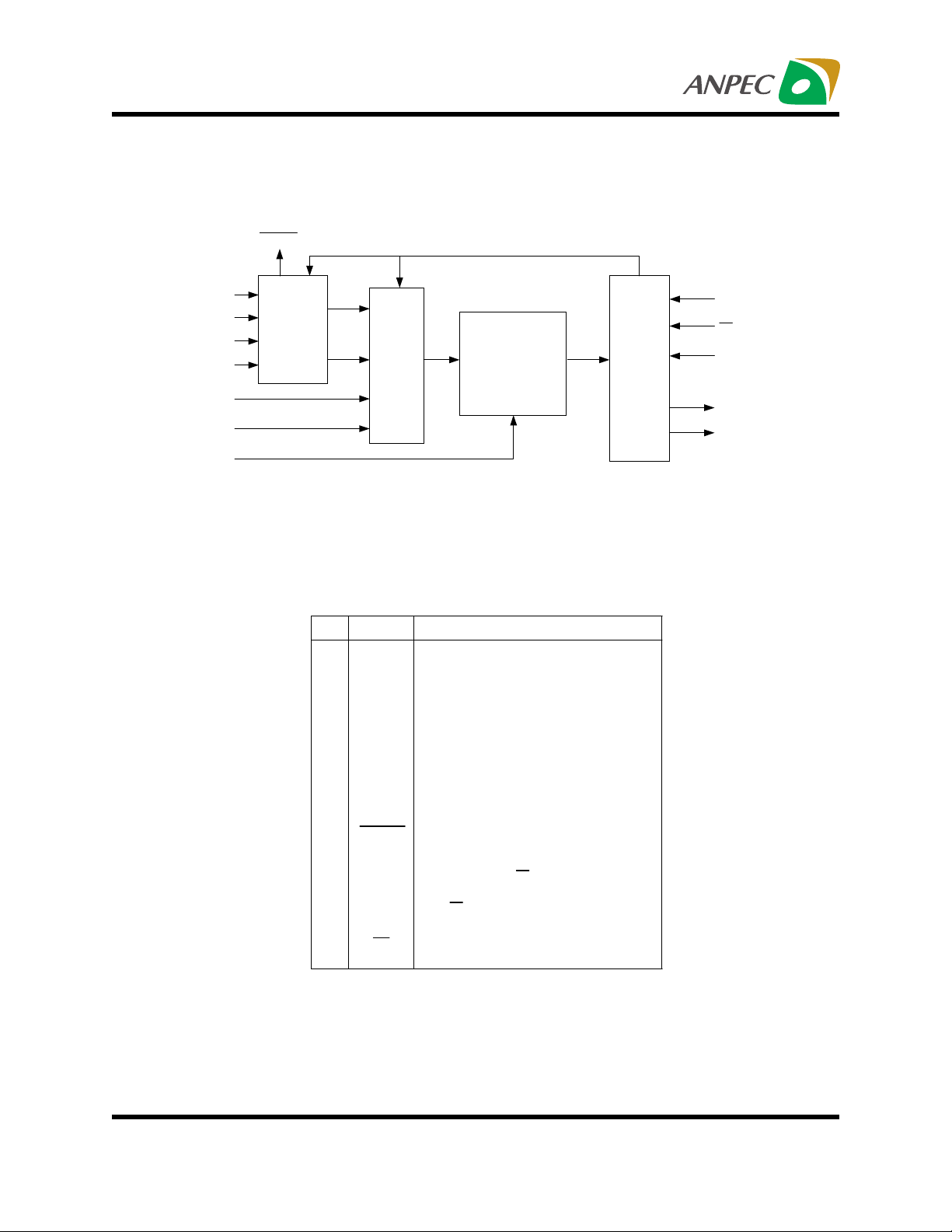
Block Diagram
PENIRQ
X+
V
X-
Y+
Y-
IN3
IN4
REF
Screen Driver
Pin Descriptions
MUX
PIN NAME
1+Vcc
2X+
3Y+
4X-
5Y-
6GND
7IN3
8IN4
9V
REF
12 Bit or 8 Bit
A/D Converter
DESCRIPTION
Power Supply,2.2V to 5V.
Connect to X+ on touch screen.
Connect to Y+ on touch screen.
Connect to X- on touch screen.
Connect to Y- on touch screen.
Ground
Auxiliary Input of A/D converter.
Auxiliary input of A/D converter.
Voltage Reference Input.
Serial
Interface
10 +Vcc Power Supply,2.2V to 5V.
11 PENIRQ Pen interrupt. Open anode output (requires
10k
to 100k
pull-up resistor externall
12 DOUT Serial Data Output. This output is high
impedance when CS is HIGH.
13 BUSY Busy Output. This output is high impedance
CS
when
is HIGH.
14 DIN Serial Data input.
15 CS Chip Select. (Active Low)
16 DCLK Serial Clock.
DCLK
CS
DIN
DOUT
BUSY
Copyright ANPEC Electronics Corp.
Rev. A.8 - Apr., 2002
www.anpec.com.tw2
Page 3
APT7843
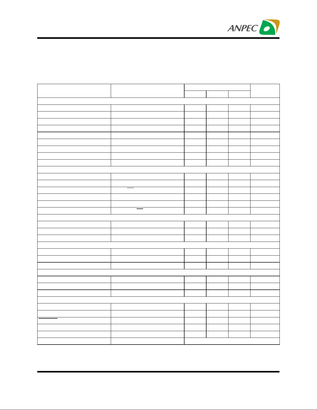
Electrical Characteristics
At TA = -40°C to 85°C , V
= +2.7V , V
CC
= +2.5V , f
REF
= 125kHz , f
SAMPLE
CLK
= 16 • f
= 2MHz , 12-bit mode
SAMPLE
, and digital inputs = GND or Vcc , unless otherwise noted.
PARAMETER CONDITIONS
MIN TYP MAX
DC ACCURACY
Resolution 12 Bits
No missing code 11 Bits
Integral Nonlinearity
Offset E rro r
Offset E rro r M atch 0.1 1 LS B
Gain Error
Gain Error Match 0.1 1 LSB
Noise 30 uV rms
Power Supply Rejection 70 dB
REFERANCE INPUT
V
Input Voltage Range 1.0 Vcc
REF
DC Leakage Current
V
Input Impedance CS = GND or Vcc 5
REF
V
Input Current 13 40
REF
F
= 12.5 kH z 2.5
SAMPLE
CS = Vcc 3
DYNAMIC PERFORENCE
Aperture Delay 30 ns
Aperture Jitter 100 ps
Channel to Channel Isolation VIN = 2.5Vp-p ; FIN = 50kHz 100 dB
CONVERSION RATE
Conversion Time 12 DCLK cycles
Track/H old A cqu isition Time 3 DCLK cycles
Throughput Rate 125 KSPS
SWITCH DRIVERS
On-Resistance
Y+ , X+ 415
Y- , X- 415
LOGIC OUTPUTS
Output High Voltage , V
Output Low Voltage , V
OH
OL
PENIRQ output low voltage , V
OL
|IOH| ≤ -250µA Vcc–0.2 V
|IOL| ≤ 250µA
Floating-State Leakage Current
Floating-State Output Capacitance 10 pF
Output Coding Straight ( Natural ) Binary
APT7843
1
±
UNITS
2LSB
±
6LSB
±
4LSB
±
A
µ
G
Ω
A
µ
A
µ
A
µ
Ω
Ω
0.4 V
0.2 V
±
10
A
µ
Note : (1) LSB means least Significant Bit. With V
Copyright ANPEC Electronics Corp.
Rev. A.8 - Apr., 2002
equal to +2.5V , one LSB is 610µV
REF
www.anpec.com.tw3
Page 4

APT7843
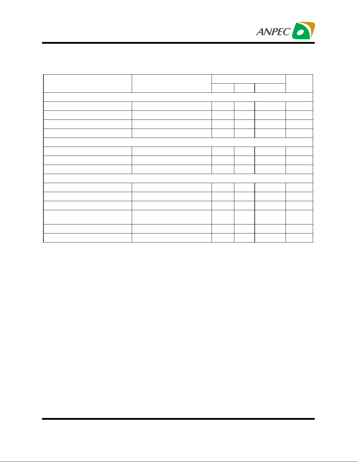
Electrical Characteristics (Cont.)
PARAMETER CONDITIONS
APT7843
MIN TYP MAX
UNITS
LOGIC INPUTS
Input High Voltage ,
V
INH
Input Low Voltage ,
V
INL
Input Current , I
IN
Input Capacitance ,
C
IN
|I
| ≤ +5µA2.4 V
INH
|I
| ≤ +5µA0.8V
INL
1
±
µ
10 pF
ANALOG INPUT
Input Voltage Ranges 0 V
DC Leakage Current
0.1
±
REF
Volts
µ
Input Capacitance 30 pF
POWER REQUIREMENTS
Vcc 2.7 3.6 V
Icc Digital I/Ps =0V or Vcc
Normal Mode (Static) Vcc = 3.6V 650
Normal Mode (F
12.5kSPS)
Shutdown
Mode(Static)
SAMPLE
=
Vcc = 3.6V 540
3
Showdown Vcc = 3.6V 3.6
µ
µ
µ
µ
A
A
A
A
A
W
Copyright ANPEC Electronics Corp.
Rev. A.8 - Apr., 2002
www.anpec.com.tw4
Page 5

APT7843
Electrical Characteristics
At TA = -40°C to 85°C, V
= +2.4V , V
CC
don’t care, f
REF
= 1.25KHz, f
SAMPLE
CLK
= 16 • f
= 20KHz, 8-bit
SAMPLE
differential mode, no support single end mode, and digital inputs = GND or Vcc , unless otherwise noted.
PARAMETER CONDITIONS
MIN TYP MAX
APT7843
UNITS
DC ACCURACY
Resolution 8 Bits
No missing code 7 Bits
Integral Nonlinearity
Offset Error
2LSB
±
6LSB
±
Offset Error Match 0.1 1 LSB
Gain Error
4LSB
±
Gain Error Match 0.1 1 LSB
Noise 30 uV rms
Power Supply Rejection 70 dB
DYNAMIC PERFORENCE
Aperture Delay 30 ns
Aperture Jitter 100 ps
Channel to Channel Isolation VIN = 2.5Vp-p ; FIN = 50kHz 100 dB
CONVERSION RATE
Conversion Time 12 DCLK cycles
Track/Hold Acquisition Time 3 DCLK cycles
Throughput Rate 1.25 KSPS
SWITCH DRIVERS
On-Resistance
Y+ , X+ 4
Y- , X- 4
Ω
Ω
LOGIC OUTPUTS
Output High Voltage , V
Output Low Voltage , V
OH
OL
PENIRQ output low voltage , V
Floating-State Leakage Current
OL
|IOH| ≤ -250µA Vcc–0.2 V
|IOL| ≤ 250µA0.4V
0.2 V
±
10
A
µ
Floating-State Output Capacitance 10 pF
Output Coding Straight ( Natural ) Binary
Copyright ANPEC Electronics Corp.
Rev. A.8 - Apr., 2002
www.anpec.com.tw5
Page 6
APT7843
Electrical Characteristics (Cont.)
PARAMETER CONDITIONS
APT7843
MIN TYP MAX
UNITS
LOGIC INPUTS
Input High Voltage , V
Input Low Voltage , V
Input Current , I
IN
Input Capacitance , C
INH
INL
IN
|I
| ≤ +5µA2.2 V
INH
|I
| ≤ +5µA0.6V
INL
+0.2 V
DD
1
±
µ
10 pF
ANALOG INPUT
Input Voltage Ranges 0 V
DC Leakage Current
0.1
±
REF
Volts
µ
Input Capacitance 30 pF
POWER REQUIREMENTS
Vcc 2.2 2.4 3.6 V
Icc Digital I/Ps =0V or Vcc
Normal Mode (Static) Vcc = 2.4V 280 650
Norm al Mode (F
12.5kSPS)
SAMPLE
=
Vcc = 2.4V 540
Shutdown Mode(Static) 3
Showdown Vcc = 2.4V 3.6
µ
µ
µ
µ
A
A
A
A
A
W
Copyright ANPEC Electronics Corp.
Rev. A.8 - Apr., 2002
www.anpec.com.tw6
Page 7

APT7843
Chip Overview
The APT7843 is a successive approximation analogto-digital (A/D) converter based around a capacitive
redistribution DAC. Figure 1 show basic operation of
the APT7843.
The APT7843 communicates via a 4-wire serial
interface. The device also requires an external reference voltage Vref. The value of the reference voltage
directly sets the input range of the converter.
The APT7843 primary function is to control resistive
touchscreens. When a touch is detected , pen interrupt pin will go low to wake up extenal microprocess.
The microprocessor writes register to initiate
conversion.
This A/D converter may also be used to measure
voltage presented on the IN3 , IN4 pins.
+2.2V to +5V
Analog Input
The analog input to the converter is provided via a
four-channel multiplexer. Figure 2 shows a simplified
diagram of the APT7843 with the difference input of
the A/D converter , and the converter’s reference.
Table I and Table II also show the relationship between
the A2 , A1 , A0 , SER/ and the configuration of
the APT7843. See the section of single-ended reference mode and differential reference mode for more
details.
DFR
1uF
to
10uF
(Optional)
Auxiliary Input
APT7843
+Vcc
X+
Y+
X-
Y-
GND
IN3
IN4 V
DCLK
BUSY
DOUT
PENIRQ
To
Touch
Screen
0.1uF
1
2
3
4
5
6
7
8
FIGURE 1. Basic Operation of the APT7843
CS
DIN
+Vcc
REF
16
15
14
13
12
11
10
9
0.1uF
Connect to
Microprossor
100k ohm (optional)
Copyright ANPEC Electronics Corp.
Rev. A.8 - Apr., 2002
www.anpec.com.tw7
Page 8

APT7843
X+
X-
Y+
Y-
IN3
IN4
GND
PENIRQ
+Vcc
V
REF
A2-A0
(Shown 001
)
(Shown HIGH)
B
SER/DFR
+IN
-IN
+REF
CONVERTER
-REF
FIGURE 2. Simplified Diagram of Analog Input
A2 A1 A0 X+ Y+ IN3 IN4 -IN X SWITCHES Y SWITCHES +REF -REF
001+IN GNDOFF ON +V
1 0 1 +IN GND ON OFF +V
0 1 0 +IN GND OFF OFF +V
1 1 0 +IN GND OFF OFF +V
TABLE I. Input C onfiguration, Single-Ended Reference Mode (SER/
A2 A1 A0 X+ Y+ IN3 IN4 -IN X SWITCHES Y SWITCHES +REF -REF
0 0 1 +IN -Y OFF ON +Y -Y
1 0 1 +IN -X ON OFF +X -X
0 1 0 +IN GND OFF OFF +V
1 1 0 +IN GND OFF OFF +V
TABLE II. Input Configuration, Differential Reference Mode (SER/
DFR
DFR
HIGH).
LOW).
REF
REF
REF
REF
REF
REF
GND
GND
GND
GND
GND
GND
Copyright ANPEC Electronics Corp.
Rev. A.8 - Apr., 2002
www.anpec.com.tw8
Page 9

APT7843
Single-Ended reference mode
Figure 3 shows the diagram of single-ended reference mode.
This application shows the measurement of current
Y poisition is made by connecting the X+ input to the
A/D converter, turning on the Y+ and Y- drivers, and
digitizing the voltage on X+ . For this measurement,
the resistance in the X+ lead does not affect the conversion. However, since the resistance between Y+
and Y- is fairly low, the on-resistance of the Y drivers
does make a small difference. Under the situation outlined so far, it would not be possible to achieve a zero
volt input or a full-scale input regardless of where the
pointing device is on the touch screen because some
voltage is lost across the internal switches. This situation can be remedied if use differential reference mode
+Vcc
Y+
V
REF
X+
+IN
+REF
Converter
-IN
-REF
Y-
Y Switch ON
GND
GND
FIGURE 3.Single-Ended Reference Mode
(SER/ High, A2=Low,A1=Low,A0=High)
DFR
Differential reference mode
As shown in Figure 4,by setting the SER/ bit
LOW, the +REF and -REF inputs are connected directly to Y+ and Y-. This makes the analog-to- digital
conversion ratiometric.
The result of the conversion is always a percentage
of the external resistance, reardless of how it changes
in relation to the on-resistance of the internal switches.
Note that there is an important consideration regarding power dissipation when using the ratiometric mode
of operation,the external device should powered
throughout the acquisition and conversion periods.
DFR
+Vcc
Y+
Y+
X+
+IN
+REF
Converter
-IN
-REF
Y-
Y Switch ON
GND
Y-
Figure 4. Differential Reference Mode
(SER/ LOW, A2=Low,A1=Low,A0=High)
DFR
Serial Interface
Data is written to,and read from , the APT7843 via
the serial port. The serial port has 4 pins - serial
clock (DCLK),chip select ( ) ,data in (DIN) and
data out (DOUT). The DCLK acts on the rising edge.
CS
The acts as a reset for the serial port with goes
low initating a conversion cycle. The cycle consists
of 2 parts - a write followed by a read. Figure 5
shows the typical timing of the APT7843’s serial
interface. A total of 24 clock cycles will complete
one conversion.
Also shown in Figure 5 is the placement and order of
the control bits within the control byte. Tables III and
IV give detailed information about these bits.
The first bit, the ′S′ bit, must always be HIGH and
indicates the start of the control byte. The APT7843
will ignore inputs on the DIN pin until the start bit S
detected.
The next three bits (A2 - A0) select the active input
channel or channels of the input multiplexer (see Tables
I and II and Figure 2).
The MODE bit determines the number of bits for each
conversion, either 12 bits (LOW) or 8 bits (HIGH).
The SER/ bit controls the reference mode: either
DFR
single-ended (HIGH) or differential (LOW). (The differential mode is also referred to as the ratiometric
conversion mode.)
The last two bits (PD1 - PD0) select the power- down
mode as shown in Table V. If both inputs are HIGH,
the device is always powered up. If both inputs are
LOW, the device enters a power-down mode between conversions.
CS
CS
Copyright ANPEC Electronics Corp.
Rev. A.8 - Apr., 2002
www.anpec.com.tw9
Page 10

APT7843
Bit 7 Bit 6 Bit 5 Bit 4 Bit 3 Bit 2 Bit 1 Bit 0
(MSB) (LSB)
SA2A1A0MODESER/DFRPD1PD0
TABLE III. Order of the Control Bits in the Control
Byte.
BIT NAME DESCRIPTION
7 S Start Bit. Control byte starts with first HIGH bit on
DIN. A new control byte can start every 15th clock
cycle in 12-bit conversion mode or every 11th clock
cycle in 8-bit conversion mode.
6-4 A2-A0 Channel Select Bits. Along with the SER/DFR bit,
these bits control the setting of the multiplexer
input, switches, and reference inputs, as detailed in
Tables I and II.
MODE 12-Bit/8-Bit Conversion Select Bit. This bit controls
the number of bits for the following conversion: 12bits(LOW) or 8-bits(HIGH).
2 SER/DFR Single-End ed/Differential Reference Select B it.
Along with bits A2-A 0, this bit controls the setting of
the multiplexer input, switches, and reference
inputs, as detailed in Tables I and II.
1-0 PD1-PD0 Power-Down Mode Select Bits. See Table V for
details.
TABLE IV. Descriptions of the Control Bits within the
Control Byte.
PD1 PD0 PENIRQ DESCRIPTION
0 0 Enabled Power-down between conversions. When
each conversion is finished, the converter
enters a low power mode.
0 1 Enabled Reserved for future use
1 0 Enabled Reserved for future use.
1 1 Disabled No power-down between conversions,
device is always powered.
TABLE V. Power-Down Selection.
CS
DCLK
DIN
1818 81
t
ACQ
SER/
MODE
S
(START)
A2 A1 A0
ldle Acquire Conversion ldle
DFR
PD1 PD0
BUSY
DOUT
11 10 9 8 7 6 5 4 3 2 1 0
(MSB) (LSB)
FIGURE 5. Conversion Timing, 24-Clocks per Conversion, 8-bit Bus Interface. No DCLK Delay Required
with Dedicated Serial Port.
Copyright ANPEC Electronics Corp.
Rev. A.8 - Apr., 2002
www.anpec.com.tw10
Page 11

APT7843
CS
DCLK
1 81 81 81
DIN
BUSY
DOUT
SS
CONTROL BITS
11 1098765
CONTROL BITS
34
11 10
012
9
FIGURE 6. Conversion Timing, 16-Clocks per Conversion, 8-bit Bus Interface. No DCLK Delay Required
with Dedicated Serial Port.
16-Clocks or 15-Clocks per Con-
AC Timing
version
Figure 8 and Table VI provide detailed timing of the
The APT7843 will alow a conversion every 16 clock
cycles, as shown in Figure 6. This figure shows
possible serial communication occurring with other
serial peripherals between each byte transfer between
the processor and the converter.
Figure 7 provides the fastest way to clock the
APT7843. This method will not work with the serial
interface of most microcontrollers and digital signal
processors as they are generally not capable of providing 15 clock cycles per serial transfer. However,
this method could be used with field programmable
gate arrays (FPGAs) or application specific integrated
circuits (ASICs). (Note that this effectively increases
the maximum conversion rate of the converter).
APT7843. Table VII provide detailed timing of low power
VCC=2.4V.
Copyright ANPEC Electronics Corp.
Rev. A.8 - Apr., 2002
www.anpec.com.tw11
Page 12

APT7843
SYMBOL DESCRIPTION MIN TYP MAX UNIT
t
ACQ
t
DS
t
DH
t
DO
t
DV
t
TR
t
CSS
t
CSH
t
CH
t
CL
t
BD
t
BDV
t
BTR
Acquisition Time 1.5
DIN Valid Prior to DCLK Rising 100 ns
DIN Hold After DCLK HIGH 10 ns
DCLK Falling to DOUT Vaild 200 ns
CS Falling to DOUT Enabled 200 ns
CS Rising to DOUT Disabled 200 ns
CS Falling to DCLK Rising 100 ns
CS Rising to DCLK lgnored 0 ns
DCLK HIGH 200 ns
DCLK LOW 200 ns
DCLK Falling to BUSY Rising 200 ns
CS Falling to BUSY Enabled 200 ns
CS Rising to BUSY Disable 200 ns
µs
TABLE VI. Timing Specifications (+Vcc=+2.7V and
Above, TA=-40°C to +85°C, CLOAD=50pF).
CS
SYMBOL DESC RIPTION MIN TYP MAX UNIT
t
ACQ
t
DS
t
DH
t
DO
t
DV
t
TR
t
CSS
t
CSH
t
CH
t
CL
t
BD
t
BDV
t
BTR
Acquisition Time 20
DIN Valid Prior to DCLK Rising 400 ns
DIN Hold After DCLK HIGH 20 ns
DCLK Falling to DOUT Vaild 400 ns
CS Falling to DOUT Enabled 400 ns
CS Rising to DOU T Disabled 400 ns
CS Falling to DC LK Rising 200 ns
CS Rising to DCLK lgnored 0 ns
DCLK HIGH 2.5
DCLK LOW 2.5
DCLK Falling to BUSY Rising 400 ns
CS Falling to BUSY Enabled 400 ns
CS Rising to BUSY Disable 400 ns
s
µ
s
µ
s
µ
TABLE VI. Timing Specifications (+Vcc=+2.4V and
Above, TA=-40°C to +85°C, CLOAD=50pF).
DCLK
1 11515 1
SGL/
MODE
DIN
A2 A1 A0
SS
DIF
PD1 PD0
A1 A0
BUSY
DOUT
11
886
10 9 7 6 5 01
2
34
FIGURE 7. Maximum Conversion Rate, 15-Clocks per Conversion.
MODE
SGL/
DIF
PD1 PD0
11 10 9
A1 A0A2 A2
S
75432
Copyright ANPEC Electronics Corp.
Rev. A.8 - Apr., 2002
www.anpec.com.tw12
Page 13

APT7843
CS
t
CSS
t
CH
DCLK
t
DS
DIN
t
BDV
BUSY
t
DV
DOUT
FIGURE 8. Detailed Timing Diagram.
t
CL
t
BD
t
DH
t
BD
t
BD
t
CSH
PD0
t
BTR
t
TR
11 10
Copyright ANPEC Electronics Corp.
Rev. A.8 - Apr., 2002
www.anpec.com.tw13
Page 14

APT7843
Packaging Information
SSOP
D
N
12
3
GAUGE
EH
PLANE
A
e
Millimeters Variations- D Inches Variations- D
Dim
A1
φ
Min. Max. Variations Min. Max.
A1.350
0.10 0.25
0.20 0.30
B
D See variations D See variations
3.75 4.05
E
e 0.625 TYP. e 0.025 TYP.
5.75 6.25
H
0.4 1.27
L
N See variations N See variations
10°8
1.75
°φ
B
SSOP-16
A1
4.75 5.05
Dim
Min. Max. Variations Min. Max.
A 0.053 0.069 SSOP-16 0.187 0.199
A1 0.004 0.010
B 0.008 0.012
E 0.147 0.160
H 0.226 0.246
L 0.016 0.050
10°8
L
°
1
Copyright ANPEC Electronics Corp.
Rev. A.8 - Apr., 2002
www.anpec.com.tw14
Page 15

APT7843
φ
φ
φ
Packaging Information
TSSOP
e
N
2 x E / 2
Dim
E1 E
12
3
b
e/2
D
A2
A1
0.25
A
(3)
Millimeters Inches
Min. Max. Min. Max.
(2)
GAUGE
PLANE
L
A 1.2 0.047
A1 0.00 0.15 0.000 0.006
A2 0.80 1.05 0.031 0.041
b 0.19 0.30 0.007 0.011
4.9 (N=16PIN)
D
6.4 (N=20PIN)
7.7 (N=24PIN)
9.6 (N=28PIN)
5.1 (N=16PIN)
6.6 (N=20PIN)
7.9 (N=24PIN)
9.8 (N=28PIN)
0.193 (N=16PIN)
0.252 (N=20PIN)
0.303 (N=24PIN)
0.378 (N=28PIN)
0.201 (N=16PIN)
0.260 (N=20PIN)
0.311 (N=24PIN)
0.386 (N=28PIN)
e 0.65 BSC 0.026 BSC
E
E1
4.30 4.50 0.169 0.177
6.40 BSC 0.252 BSC
L 0.45 0.75 0.018 0.030
10
212
312
°
REF 12° REF
°
REF 12° REF
°
8
°
0
°
8
1
°
Copyright ANPEC Electronics Corp.
Rev. A.8 - Apr., 2002
www.anpec.com.tw15
Page 16

APT7843
Physical Specifications
Terminal Material Solder-Plated Copper (Solder Material : 90/10 or 63/37 SnPb)
Lead Solderability Meets EIA Specification RSI86-91, ANSI/J-STD-002 Category 3.
Reflow Condition (IR/Convection or VPR Reflow)
Peak temperature
temperature
Pre-heat temperature
°
183 C
Time
Classification Reflow Profiles
Convection or IR/
Convection
Average ramp-up rate(183°C to Peak) 3°C/second max. 10 °C /second max.
Preheat temperature 125 ± 25°C)
Temperature maintained above 183°C
Time within 5°C of actual peak temperature
Peak temperature range
Ramp-down rate
Time 25°C to peak temperature
120 seconds max
60 – 150 seconds
10 –20 seconds 60 seconds
220 +5/-0°C or 235 +5/-0°C 215-219°C or 235 +5/-0°C
6 °C /second max. 10 °C /second max.
6 minutes max.
VPR
Package Reflow Conditions
pkg. thickness ≥≥≥≥ 2.5mm
and all bgas
Convection 220 +5/-0 °C Convection 235 +5/-0 °C
VPR 215-219 °C VPR 235 +5/-0 °C
IR/Convection 220 +5/-0 °C IR/Convection 235 +5/-0 °C
Copyright ANPEC Electronics Corp.
Rev. A.8 - Apr., 2002
pkg. thickness < 2.5mm and
pkg. volume ≥≥≥≥ 350 mm³
pkg. thickness < 2.5mm and pkg.
volume < 350mm³
www.anpec.com.tw16
Page 17

APT7843
Reliability test program
Test item Method Description
SOLDERABILITY MIL-STD-883D-2003 245°C,5 SEC
HOLT MIL-STD 883D-1005.7 1000 Hrs Bias @ 125°C
PCT JESD-22-B, A102 168 Hrs, 100% RH, 121°C
TST MIL-STD 883D-1011.9 -65°C ~ 150°C, 200 Cycles
Carrier Tape & Reel Dimensions
t
W
E
F
Po
A
P
P1
Ao
J
D
Bo
D1
C
Ko
T2
B
T1
Application
SSOP-14/16
Copyright ANPEC Electronics Corp.
Rev. A.8 - Apr., 2002
A B D0 D1 E F P0 P1 P2
6.95 5.4 1.55±0.05 1.55±0.1 1.75±0.1 5.5±0.05 4.0±0.1 8.0±0.1 2.0±0.05
T T2 W W1 C1 C2 T1 T2 C
0.3±0.05 2.2 12.0±0.3 9.5 13±0.3 21±0.8 13.5±0.5 2.0±0.2 80±1
(mm)
www.anpec.com.tw17
Page 18

APT7843
Customer Service
Anpec Electronics Corp.
Head Office :
5F, No. 2 Li-Hsin Road, SBIP,
Hsin-Chu, Taiwan, R.O.C.
Tel : 886-3-5642000
Fax : 886-3-5642050
Taipei Branch :
7F, No. 137, Lane 235, Pac Chiao Rd.,
Hsin Tien City, Taipei Hsien, Taiwan, R. O. C.
Tel : 886-2-89191368
Fax : 886-2-89191369
Copyright ANPEC Electronics Corp.
Rev. A.8 - Apr., 2002
www.anpec.com.tw18
 Loading...