

Page 1
APT50M75JLLU2
APT50M75JLLU2
500V 51A 0.075W
POWER MOS 7
TM
S
K
Power MOS 7TM is a new generation of low loss, high voltage, N-Channel
51
51
50
D
®
D
S
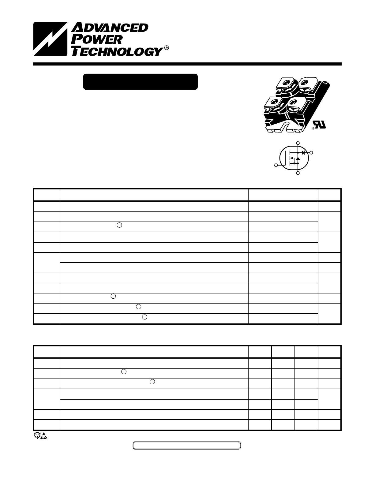
SOT-227
"UL Recognized"
K
UNIT
Volts
Amps
Volts
Watts
W/°C
°C
Amps
mJ
enhancement mode power MOSFETS. Both conduction and switching
losses are addressed with Power MOS 7
and Qg. Power MOS 7
TM
combines lower conduction and switching losses
TM
by significantly lowering R
DS(ON)
G
along with exceptionally fast switching speeds inherent with APT's
patented metal gate structure.
ISOTOP
• Lower Input Capacitance • Increased Power Dissipation
• Lower Miller Capacitance •Easier To Drive
G
• Lower Gate Charge, Qg •PFC "Boost" Configuration
MAXIMUM RATINGS All Ratings: TC = 25°C unless otherwise specified.
Symbol
V
DSS
I
D
I
DM
V
GS
V
GSM
P
D
TJ,T
STG
T
L
I
AR
E
AR
E
AS
Parameter
Drain-Source Voltage
Continuous Drain Current @ T
Pulsed Drain Current
Gate-Source Voltage Continuous
Gate-Source Voltage Transient
Total Power Dissipation @ TC = 25°C
Linear Derating Factor
Operating and Storage Junction Temperature Range
Lead Temperature: 0.063" from Case for 10 Sec.
Avalanche Current
Repetitive Avalanche Energy
ADVANCE TECHNICAL
Single Pulse Avalanche Energy
1
1
(Repetitive and Non-Repetitive)
INFORMATION
= 25°C
C
1
4
APT50M75JLLU2
500
204
±30
±40
465
3.72
-55 to 150
300
2500
STATIC ELECTRICAL CHARACTERISTICS
Symbol
BV
I
D(on)
R
DS(on)
I
DSS
I
GSS
V
GS(th)
USA 405 S.W. Columbia Street Bend, Oregon 97702 -1035 Phone: (541) 382-8028 FAX: (541) 388-0364
EUROPE Chemin de Magret F-33700 Merignac - France Phone: (33)5 57 92 15 15 FAX: (33)5 5647 9761
Characteristic / Test Conditions
Drain-Source Breakdown Voltage (V
DSS
On State Drain Current
Drain-Source On-State Resistance
Zero Gate Voltage Drain Current (VDS = V
Zero Gate Voltage Drain Current (V
Gate-Source Leakage Current (VGS = ±30V, V
Gate Threshold Voltage (VDS = VGS, ID = 2.5mA)
CAUTION: These Devices are Sensitive to Electrostatic Discharge. Proper Handling Procedures Should Be Followed.
2
(V
DS
APT Website - http://www.advancedpower.com
= 0V, ID = 250µA)
GS
> I
x R
D(on)
2
(VGS = 10V, 0.5 I
= 0.8 V
DS
Max, VGS = 10V)
DS(on)
D[Cont.]
, VGS = 0V)
DSS
, VGS = 0V, TC = 125°C)
DSS
= 0V)
DS
)
MIN TYP MAX
500
51
35
0.075
100
500
±100
UNIT
Volts
Amps
Ohms
µA
nA
Volts
050-7095 Rev - 10-2001
Page 2
DYNAMIC CHARACTERISTICS
Note:
Duty Factor D =
t
1
/
t
2
Peak TJ = PDM x Z
θJC
+ T
C
t
1
t
2
P
DM
APT50M75JLLU2
Symbol
C
C
C
Q
Q
Q
t
d(on)
t
d(off)
Characteristic
Input Capacitance
iss
Output Capacitance
oss
Reverse Transfer Capacitance
rss
Total Gate Charge
g
Gate-Source Charge
gs
Gate-Drain ("Miller") Charge
gd
Turn-on Delay Time
t
Rise Time
r
Turn-off Delay Time
t
Fall Time
f
Test Conditions
V
VDS = 25V
f = 1 MHz
3
V
GS
VDD = 0.5 V
ID = I
D[Cont.]
VGS = 15V
VDD = 0.5 V
ID = I
D[Cont.]
RG = 0.6W
SOURCE-DRAIN DIODE RATINGS AND CHARACTERISTICS
Symbol
I
I
SM
V
t
Q
dv
Characteristic / Test Conditions
Continuous Source Current (Body Diode)
S
ADVANCE TECHNICAL
Pulsed Source Current
Diode Forward Voltage 2 (VGS = 0V, IS = -I
SD
Reverse Recovery Time (IS = -I
rr
Reverse Recovery Charge (I
rr
/
Peak Diode Recovery dv/
dt
1
(Body Diode)
dt
INFORMATION
)
D[Cont.]
, dlS/dt = 100A/µs)
D[Cont.]
= -I
S
5
, dlS/dt = 100A/µs)
D[Cont.]
= 0V
GS
= 10V
DSS
@ 25°C
DSS
@ 25°C
MIN TYP MAX
5800
1200
90
145
38
66
17
14
38
5
MIN TYP MAX
51
204
1.3
620
14.7
8
UNIT
pF
nC
ns
UNIT
Amps
Volts
ns
µC
V/ns
050-7095 Rev - 10-2001
THERMAL CHARACTERISTICS
Symbol
R
qJC
R
qJA
1
Repetitive Rating: Pulse width limited by maximum junction
temperature.
2
Pulse Test: Pulse width < 380 µs, Duty Cycle < 2%
APT Reserves the right to change, without notice, the specifications and information contained herein.
Characteristic
Junction to Case
Junction to Ambient
0.3
D=0.5
0.1
0.05
0.01
0.005
, THERMAL IMPEDANCE (°C/W)
JC
q
Z
0.001
-5
10
0.2
0.1
0.05
0.02
0.01
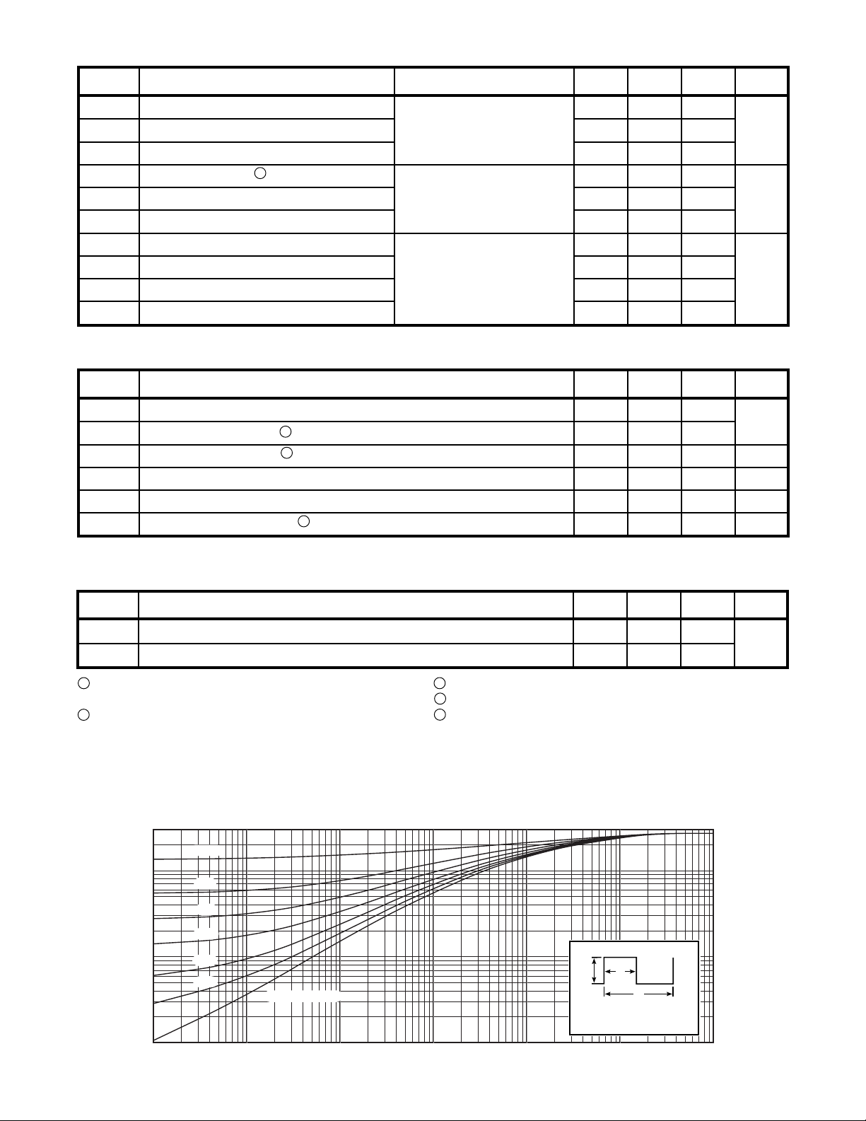
FIGURE 1, MAXIMUM EFFECTIVE TRANSIENT THERMAL IMPEDANCE, JUNCTION-TO-CASE vs PULSE DURATION
SINGLE PULSE
-4
10
3
See MIL-STD-750 Method 3471
4
Starting T
5dv
/
numbers reflect the limitations of the test circuit rather than the
dt
device itself. I
-3
10
RECTANGULAR PULSE DURATION (SECONDS)
-2
10
+25°C, L = 1.92mH, R
j
=
S
10
£ -I
-1
MIN TYP MAX
G
di
/
£ 700A/µs V
D[Cont.
dt
]
1.0 10
0.27
40
25W, Peak IL = 51A
=
£ V
R
DSS
T
UNIT
°C/W
£ 150°C
J
Page 3

APT50M75JLLU2
Diode Specifications Section
MAXIMUM RATINGS (UltraFast Recovery Diode) All Ratings: TC = 25°C unless otherwise specified.
Symbol
V
V
RRM
V
RWM
IF(AV)
(RMS)
I
F
I
FSM
TJ,T
T
Characteristic / Test Conditions
Maximum D.C. Reverse Voltage
R
Maximum Peak Repetitive Reverse Voltage
Maximum Working Peak Reverse Voltage
Maximum Average Forward Current (T
RMS Forward Current
Non-Repetitive Forward Surge Current (TJ = 45°C, 8.3mS)
Operating and StorageTemperature Range
STG
Lead Temperature: 0.063" from Case for 10 Sec.
L
STATIC ELECTRICAL CHARACTERISTICS
Symbol
V
I
RM
Characteristic / Test Conditions
ADVANCE TECHNICAL
Maximum Forward Voltage I
F
Maximum Reverse Leakage Current VR = VR Rated
INFORMATION
= 80°C, Duty Cycle = 0.5)
C
I
= 30A
F
= 60A
F
IF = 30A, TJ = 150°C
VR = VR Rated, TJ = 125°C
APT50M75JLLU2
600
30
60
320
-55 to 150
300
MIN TYP MAX
1.8
1.5
1.6
250
500
UNIT
Volts
Amps
°C
UNIT
Volts
µA
C
Junction Capacitance, V
T
= 200V
R
40
pF
050-7095 Rev - 10-2001
Page 4

DYNAMIC CHARACTERISTICS
Note:
Duty Factor D =
t
1
/
t
2
Peak TJ = PDM x Z
θJC
+ T
C
t
1
t
2
P
DM
APT50M75JLLU2
Symbol
t
rr1
t
rr2
t
rr3
t
fr1
t
fr2
I
RRM1
I
RRM2
Q
rr1
Q
rr2
V
fr1
V
fr2
diM/dt
Characteristic
Reverse Recovery Time, I
= 1.0A, diF/dt = -15A/µS, VR = 30V, TJ = 25°C
F
MIN TYP MAX
Reverse Recovery Time TJ = 25°C
= 30A, diF/dt = -240A /µS, VR = 350V TJ = 100°C
I
F
Forward Recovery Time TJ = 25°C
= 30A, diF/dt = 240A /µS, VR = 350V TJ = 100°C
I
F
155
155
Reverse Recovery Current TJ = 25°C
= 30A, diF/dt = -240A /µS, VR = 350V TJ = 100°C
I
F
Recovery Charge T
= 25°C
J
IF = 30A, diF/dt = -240A /µS, VR = 350V TJ = 100°C
Forward Recovery Voltage T
= 30A, diF/dt = 240A /µS, VR = 350V TJ = 100°C
I
F
Rate of Fall of Recovery Current TJ = 25°C
ADVANCE TECHNICAL
= 30A, diF/dt = -240A/µS, VR = 350V (See Figure 10) TJ = 100°C
I
F
INFORMATION
= 25°C
J
7.5 15
100
300
400
200
50 65
50
80
410
5
5
UNIT
nS
Amps
nC
Volts
A/µS
THERMAL AND MECHANICAL CHARACTERISTICS
Symbol
R
qJC
R
W
0.05
, THERMAL IMPEDANCE (°C/W)
JC
q
Z
0.01
Characteristic / Test Conditions
Junction-to-Case Thermal Resistance
Junction-to-Ambient Thermal Resistance
qJA
Package Weight
T
2.0
1.0
0.5
0.1
D=0.5
0.2
0.1
0.05
0.02
0.01
SINGLE PULSE
MIN TYP MAX
0.90
20
1.06
30
UNIT
°C/W
oz.
gm.
050-7095 Rev - 10-2001
0.005
-5
10
FIGURE 14, MAXIMUM EFFECTIVE TRANSIENT THERMAL IMPEDANCE, JUNCTION-TO-CASE vs PULSE DURATION
-4
10
-3
10
RECTANGULAR PULSE DURATION (SECONDS)
-2
10
10
-1
1.0 10
Page 5

APT50M75JLLU2
100
80
60
40
, FORWARD CURRENT
F
20
TJ = 150°C
TJ = 100°C
TJ = 25°C
TJ = -55°C
1600
1200
, REVERSE RECOVERY CHARGE
rr
800
400
TJ=100°C
VR=350V
60A
30A
15A
0
0 0.5 1.0 1.5 2.0 2.5 10 50 100 500 1000
Figure 15, Forward Voltage Drop vs Forward Current Figure 16, Reverse Recovery Charge vs Current Slew Rate
, REVERSE RECOVERY CURRENT I
RRM
Figure 17, Reverse Recovery Current vs Current Slew Rate Figure 18, Dynamic Parameters vs Junction Temperature
, REVERSE RECOVERY TIME I
rr
Figure 19, Reverse Recovery Time vs Current Slew Rate Figure 20, Forward Recovery Voltage/Time vs Current Slew Rate
VF, ANODE-TO-CATHODE VOLTAGE (VOLTS) diF/dt, CURRENT SLEW RATE (AMPERES/µSEC)
40
TJ=100°C
VR=350V
30
20
10
0
0 200 400 600 800 1000 -50 -25 0 25 50 75 100 125 150
diF/dt, CURRENT SLEW RATE (AMPERES/µSEC) TJ, JUNCTION TEMPERATURE (°C)
200
TJ=100°C
VR=350V
160
120
80
40
0
0 200 400 600 800 1000 0 200 400 600 800 1000
/dt, CURRENT SLEW RATE (AMPERES/µSEC) diF/dt, CURRENT SLEW RATE (AMPERES/µSEC)
di
F
800
30A
ADVANCE TECHNICAL
60A
30A
15A
60A
15A
, DYNAMIC PARAMETERS Q
INFORMATION
f
, FORWARD RECOVERY TIME K
fr
t
0
2.0
1.6
1.2
0.8
0.4
0.0
2500
2000
1500
1000
(nano-SECONDS) (NORMALIZED) (nano-COULOMBS)
500
I
TJ=100°C
VR=350V
IF=30A
0
RRM
Q
rr
t
rr
t
rr
Q
rr
25
20
V
fr
t
fr
15
10
5
0
(VOLTS)
, FORWARD RECOVERY VOLTAGE
fr
V
500
100
(pico-FARADS) (nano-SECONDS) (AMPERES) (AMPERES)
, JUNCTION CAPACITANCE t
J
C
50
30
0.01 0.05 0.1 0.5 1 5 10 50 100 200
Figure 21, Junction Capacitance vs Reverse Voltage
V
, REVERSE VOLTAGE (VOLTS)
R
050-7095 Rev - 10-2001
Page 6

30µH
V
r
APT50M75JLLU2
D.U.T.
t
Q
/
rr
rr
Waveform
+15v
diF/dt Adjust
0v
-15v
Figure 22, Diode Reverse Recovery Test Circuit and Waveforms
1
- Forward Conduction Current
I
F
di
2
/dt - Current Slew Rate, Rate of Forward
F
Current Change Through Zero Crossing.
1
Zero
3
4
5
6
- Peak Reverse Recovery Current.
I
RRM
trr - Reverse Recovery Time Measured from Point of I
Current Falling Through Zero to a Tangent Line
ADVANCE TECHNICAL
Extrapolated Through Zero Defined by 0.75 and 0.50 I
Qrr - Area Under the Curve Defined by I
INFORMATION
and trr.
RRM
F
6
{
diM/dt
RRM
}
.
diM/dt - Maximum Rate of Current Change During the Trailing Portion of t
Figure 23, Diode Reverse Recovery Waveform and Definitions
PEARSON 411
CURRENT
TRANSFORMER
3
2
rr.
4
6
5
0.5 I
RRM
0.75 I
RRM
Q
rr
= 1/
t
I
(
rr
2
)
RRM
.
r = 4.0 (.157)
(2 places)
SOT-227 (ISOTOP®) Package Outline
31.5 (1.240)
31.7 (1.248)
7.8 (.307)
8.2 (.322)
14.9 (.587)
15.1 (.594)
30.1 (1.185)
30.3 (1.193)
38.0 (1.496)
38.2 (1.504)
Dimensions in Millimeters and (Inches)
W=4.1 (.161)
W=4.3 (.169)
H=4.8 (.187)
H=4.9 (.193)
(4 places)
4.0 (.157)
4.2 (.165)
(2 places)
3.3 (.129)
3.6 (.143)
Cathode Drain
Source
11.8 (.463)
12.2 (.480)
8.9 (.350)
9.6 (.378)
0.75 (.030)
0.85 (.033)
1.95 (.077)
2.14 (.084)
Hex Nut M4
(4 places)
12.6 (.496)
12.8 (.504)
Changed 2/10/99
Gate
25.2 (0.992)
25.4 (1.000)
®
ISOTOP
is a Registered Trademark of SGS Thomson.
APT's devices are covered by one or more of the following U.S.patents: 4,895,810 5,045,903 5,089,434 5,182,234 5,019,522 5,262,336
050-7095 Rev - 10-2001
5,256,583 4,748,103 5,283,202 5,231,474 5,434,095 5,528,058
"UL Recognized" File No. E145592
 Loading...