

Page 1
1 3
2
1-Anode 1
2-Common Cathode
3-Anode 2
1
2
3
APT30D40HCT 400V 2x30A
ULTRAFAST SOFT RECOVERY RECTIFIER DIODES
PRODUCT APPLICATIONS
• Parallel Diode
PRODUCT FEATURES
• Ultrafast Recovery Times
PRODUCT BENEFITS
• Low Losses
-Switchmode Power Supply
-Inverters
• Free Wheeling Diode
-Motor Controllers
-Converters
• Snubber Diode
• Uninterruptible Power Supply (UPS)
• Induction Heating
• High Speed Rectifiers
• Soft Recovery Characteristics
• Hermetic TO-258 Package
• Low Forward Voltage
• High Blocking Voltage
• Low Leakage Current
• Low Noise Switching
• Cooler Operation
• Higher Reliability Systems
• Increased System Power
Density
MAXIMUM RATINGS All Ratings Are Per Leg: TC = 25°C unless otherwise specified.
Symbol
V
R
V
RRM
V
RWM
IF(AV)
(RMS)
I
F
I
FSM
TJ,T
STG
T
L
Characteristic / Test Conditions
Maximum D.C. Reverse Voltage
Maximum Peak Repetitive Reverse Voltage
Maximum Working Peak Reverse Voltage
Maximum Average Forward Current (T
RMS Forward Current
Non-Repetitive Forward Surge Current (TJ = 45°C, 8.3ms)
Operating and StorageTemperature Range
Lead Temperature: 0.063" from Case for 10 Sec.
= 85°C, Duty Cycle = 0.5)
C
APT30D40HCT
400
30
70
320
-55 to 150
300
UNIT
Volts
Amps
°C
STATIC ELECTRICAL CHARACTERISTICS
Symbol
V
I
RM
C
L
USA
405 S.W. Columbia Street Bend, Oregon 97702-1035 Phone: (541) 382-8028 FAX: (541) 388-0364
EUROPE
Avenue J.F. Kennedy Bât B4 Parc Cadéra Nord F-33700 Merignac - France Phone: (33)5 57 92 1515 FAX: (33) 5 56 47 97 61
Characteristic / Test Conditions
Maximum Forward Voltage I
F
Maximum Reverse Leakage Current VR = VR Rated
Junction Capacitance, V
T
Series Inductance (Lead to Lead 5mm from Base)
S
= 200V
R
APT Website - http://www.advancedpower.com
I
= 30A
F
= 60A
F
IF = 30A, TJ = 150°C
VR = VR Rated, TJ = 125°C
MIN TYP MAX
1.75
1.85
1.55
250
500
52
TBD
UNIT
Volts
µA
pF
nH
053-4018 Rev A
Page 2
DYNAMIC CHARACTERISTICS
APT30D40HCT
Symbol
t
rr1
t
rr2
t
rr3
t
fr1
t
fr2
I
RRM1
I
RRM2
Q
rr1
Q
rr2
V
fr1
V
fr2
diM/dt
Characteristic
Reverse Recovery Time, I
= 30A, diF/dt = -100A/µs, VR = 50V, TJ = 25°C
F
Reverse Recovery Time TJ = 25°C
= 30A, diF/dt = -240A/µs, VR = 240V TJ = 100°C
I
F
Forward Recovery Time TJ = 25°C
= 30A, diF/dt = 240A/µs, VR = 240V TJ = 100°C
I
F
Reverse Recovery Current TJ = 25°C
= 30A, diF/dt = -100A/µs, VR = 50V TJ = 100°C
I
F
Recovery Charge T
= 25°C
J
IF = 30A, diF/dt = -240A/µs, VR = 240V TJ = 100°C
Forward Recovery Voltage T
= 30A, diF/dt = 240A/µs, VR = 240V TJ = 100°C
I
F
= 25°C
J
Rate of Fall of Recovery Current TJ = 25°C
= 30A, diF/dt = -240A/µs, VR = 240V (See Figure 10) TJ = 100°C
I
F
MIN TYP MAX
40 60
45
70
150
150
2.2 5
5
135
350
3.2
3.2
500
500
UNIT
ns
Amps
nC
Volts
A/µs
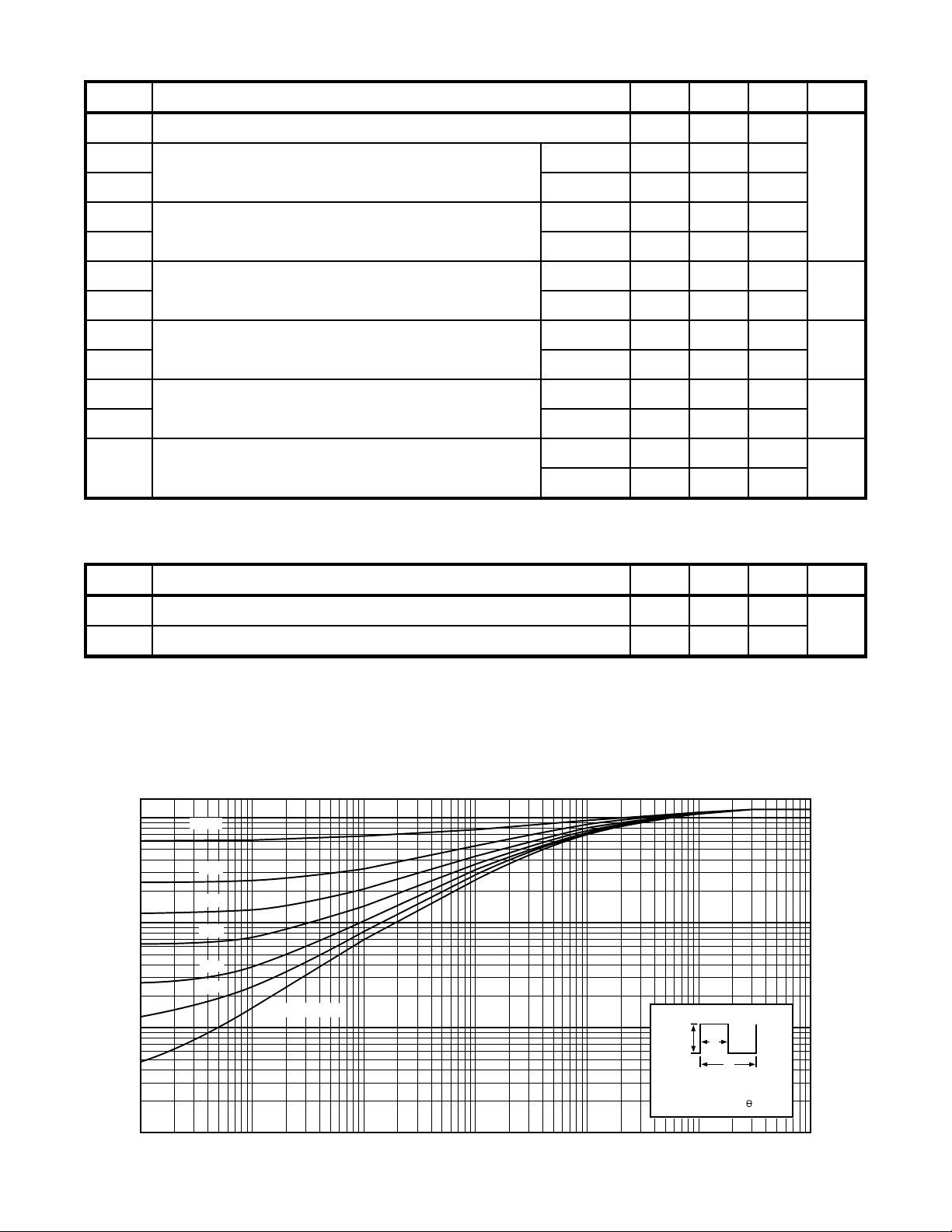
THERMAL AND MECHANICAL CHARACTERISTICS
Symbol
R
R
0.05
0.01
, THERMAL IMPEDANCE (°C/W)
JC
θ
Z
0.005
θJC
θJA
1.0
0.5
0.1
Characteristic / Test Conditions
Junction-to-Case Thermal Resistance
Junction-to-Ambient Thermal Resistance
D=0.5
0.2
0.1
0.05
0.02
0.01
SINGLE PULSE
MIN TYP MAX
1.2
40
NOTE:
DM
t
1
P
t
2
/
DUTY FACTOR D=t
=+
PEAK T P x Z T
DM JC
t
12
UNIT
°C/W
CJ
0.001
053-4018 Rev A
-5
10
FIGURE 1, MAXIMUM EFFECTIVE TRANSIENT THERMAL IMPEDANCE, JUNCTION-TO-CASE vs PULSE DURATION
-4
10
-3
10
RECTANGULAR PULSE DURATION (SECONDS)
-2
10
10
-1
1.0 10
Page 3

APT30D40HCT
100
80
60
40
, FORWARD CURRENT
F
20
TJ = 150°C
TJ = 100°C
TJ = 25°C
TJ = -55°C
1600
TJ=100°C
VR=240V
1200
800
400
, REVERSE RECOVERY CHARGE
rr
60A
30A
15A
0
0.4 0.8 1.2 1.6 2.0 2.4 10 50 100 500 1000
VF, ANODE-TO-CATHODE VOLTAGE (VOLTS) diF/dt, CURRENT SLEW RATE (AMPERES/µSEC)
0
Figure 2, Forward Voltage Drop vs Forward Current Figure 3, Reverse Recovery Charge vs Current Slew Rate
2.0
1.6
1.2
t
0.8
, DYNAMIC PARAMETERS Q
f
0.4
I
RRM
rr
Q
rr
t
rr
Q
rr
0.0
, REVERSE RECOVERY CURRENT I
RRM
50
TJ=100°C
VR=240V
40
60A
30
20
30A
15A
10
0
0 200 400 600 800 1000 -50 -25 0 25 50 75 100 125 150
di
/dt, CURRENT SLEW RATE (AMPERES/µSEC) TJ, JUNCTION TEMPERATURE (°C)
F
Figure 4, Reverse Recovery Current vs Current Slew Rate Figure 5, Dynamic Parameters vs Junction Temperature
100
TJ=100°C
VR=240V
90
80
60A
30A
15A
800
600
TJ=100°C
VR=240V
IF=30A
V
fr
400
16
12
8
70
(nano-SECONDS) (NORMALIZED) (nano-COULOMBS)
60
, REVERSE RECOVERY TIME I
rr
50
0 200 400 600 800 1000 0 200 400 600 800 1000
diF/dt, CURRENT SLEW RATE (AMPERES/µSEC) diF/dt, CURRENT SLEW RATE (AMPERES/µSEC)
200
, FORWARD RECOVERY TIME K
fr
t
t
fr
0
4
0
Figure 6, Reverse Recovery Time vs Current Slew Rate Figure 7, Forward Recovery Voltage/Time vs Current Slew Rate
1000
(VOLTS)
, FORWARD RECOVERY VOLTAGE
fr
V
500
100
50
(pico-FARADS) (nano-SECONDS) (AMPERES) (AMPERES)
, JUNCTION CAPACITANCE t
J
C
10
0.01 0.05 0.1 0.5 1 5 10 50 100 200
Figure 8, Junction Capacitance vs Reverse Voltage
V
, REVERSE VOLTAGE (VOLTS)
R
053-4018 Rev A
Page 4

30µH
V
r
APT30D40HCT
D.U.T.
t
Q
/
rr
rr
Waveform
+15v
diF/dt Adjust
0v
-15v
Figure 9, Diode Reverse Recovery Test Circuit and Waveforms
1
- Forward Conduction Current
I
F
2
/dt - Current Slew Rate, Rate of Forward
di
F
Current Change Through Zero Crossing.
1
Zero
3
4
5
6
- Peak Reverse Recovery Current.
I
RRM
trr - Reverse Recovery Time Measured from Point of I
Current Falling Through Zero to a Tangent Line
Extrapolated Through Zero Defined by 0.75 and 0.50 I
Qrr - Area Under the Curve Defined by I
RRM
and trr.
F
6
{
diM/dt
RRM
}
.
diM/dt - Maximum Rate of Current Change During the Trailing Portion of t
Figure 10, Diode Reverse Recovery Waveform and Definitions
PEARSON 411
CURRENT
TRANSFORMER
3
2
rr.
4
6
5
0.5 I
RRM
0.75 I
RRM
Q
rr
= 1/
t
I
(
rr
2
)
RRM
.
21.21 (.835)
20.70 (.815)
1.14 (.045)
0.88 (.035)
13.84 (.545)
13.58 (.535)
3.56 (.140) BSC
6.86 (.270)
6.09 (.240)
TO-258AA Package Outline
TO-258AA (Revised 3/1/90)
17.96 (.707)
17.70 (.697)
19.05 (0.750)
12.70 (0.500)
1.65 (.065)
1.39 (.055)
Dimensions in Millimeters and (Inches)
Dia. Typ.
3 Leads
5.08 (.200) BSC
17.65 (.695)
17.39 (.685)
8.89 (.350)
8.63 (.340)
4.19 (.165)
3.94 (.155)
Anode 1
Common Cathode
Anode 2
APT Reserves the right to change, without notice, the specifications and information contained herein.
053-4018 Rev A
 Loading...