

Page 1
查询APT150GN120J供应商
TYPICAL PERFORMANCE CURVES
1200V
APT150GN120J
®
APT150GN120J
C
®
E
7
2
2
-
T
O
S
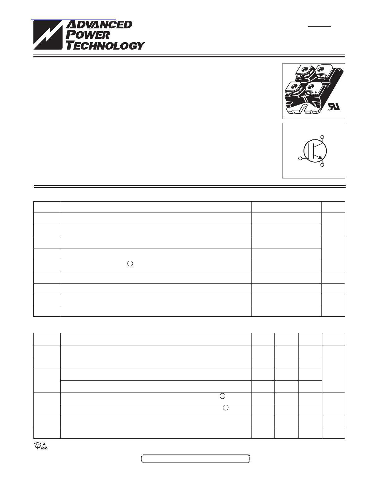
"UL Recognized"
file # E145592
Utilizing the latest Field Stop and Trench Gate technologies, these IGBT's have ultra
low V
conduction loss. Easy paralleling is a result of very tight parameter distribution and
a slightly positive V
extremely reliable operation, even in the event of a short circuit fault. Low gate charge
simplifies gate drive design and minimizes losses.
and are ideal for low frequency applications that require absolute minimum
CE(ON)
temperature coefficient. A built-in gate resistor ensures
CE(ON)
E
G
ISOTOP
• 1200V Field Stop
• Trench Gate: Low V
• Easy Paralleling
• Intergrated Gate Resistor: Low EMI, High Reliability
Applications: Welding, Inductive Heating, Solar Inverters, SMPS, Motor drives, UPS
CE(on)
G
C
E
MAXIMUM RATINGS All Ratings: TC = 25°C unless otherwise specified.
Symbol
V
CES
V
GE
I
C1
I
C2
I
CM
SSOA
P
TJ,T
T
Parameter
Collector-Emitter Voltage
Gate-Emitter Voltage
Continuous Collector Current @ TC = 25°C
Continuous Collector Current @ TC = 110°C
Pulsed Collector Current
Switching Safe Operating Area @ TJ = 150°C
Total Power Dissipation
D
Operating and Storage Junction Temperature Range
STG
Max. Lead Temp. for Soldering: 0.063" from Case for 10 Sec.
L
1
APT150GN120J
1200
±30
215
99
450
450A @ 1200V
625
-55 to 150
300
UNIT
Volts
Amps
Watts
°C
STATIC ELECTRICAL CHARACTERISTICS
Symbol
V
(BR)CES
V
GE(TH)
V
CE(ON)
I
CES
I
GES
R
G(int)
Characteristic / Test Conditions
Collector-Emitter Breakdown Voltage (VGE = 0V, IC = 6mA)
Gate Threshold Voltage (VCE = VGE, IC = 6mA, Tj = 25°C)
Collector-Emitter On Voltage (VGE = 15V, IC = 150A, Tj = 25°C)
Collector-Emitter On Voltage (VGE = 15V, IC = 150A, Tj = 125°C)
Collector Cut-off Current (VCE = 1200V, VGE = 0V, Tj = 25°C)
Collector Cut-off Current (VCE = 1200V, VGE = 0V, Tj = 125°C)
Gate-Emitter Leakage Current (VGE = ±20V)
Integrated Gate Resistor
CAUTION: These Devices are Sensitive to Electrostatic Discharge. Proper Handling Procedures Should Be Followed.
APT Website - http://www.advancedpower.com
2
2
MIN TYP MAX
1200
5.0 5.8 6.5
1.4 1.7 2.1
100
TBD
600
5
Units
Volts
2.08
µA
nA
Ω
050-7608 Rev B 11-2005
Page 2
DYNAMIC CHARACTERISTICS
Symbol
C
C
C
V
GEP
Q
Q
Q
SSOA
t
d(on)
t
d(off)
E
E
E
t
d(on)
t
d(off)
E
E
E
Characteristic
Input Capacitance
ies
Output Capacitance
oes
Reverse Transfer Capacitance
res
Gate-to-Emitter Plateau Voltage
Total Gate Charge
g
Gate-Emitter Charge
ge
Gate-Collector ("Miller ") Charge
gc
Switching Safe Operating Area
Turn-on Delay Time
t
Current Rise Time
r
Turn-off Delay Time
t
Current Fall Time
f
Turn-on Switching Energy
on1
Turn-on Switching Energy (Diode)
on2
Turn-off Switching Energy 6
off
Turn-on Delay Time
t
Current Rise Time
r
Turn-off Delay Time
t
Current Fall Time
f
Turn-on Switching Energy 4
on1
Turn-on Switching Energy (Diode)
on2
Turn-off Switching Energy
off
3
APT150GN120J
Test Conditions
Capacitance
V
= 0V, V
GE
CE
= 25V
f = 1 MHz
Gate Charge
V
= 15V
GE
V
= 600V
CE
IC = 150A
TJ = 150°C, RG = 4.3Ω 7, V
15V, L = 100µH,V
= 1200V
CE
Inductive Switching (25°C)
V
= 800V
CC
V
= 15V
GE
IC = 150A
4
5
RG = 1.0Ω
TJ = +25°C
7
MIN TYP MAX
9500
500
400
9.5
800
70
430
=
GE
450
55
65
675
85
22
27
UNIT
pF
V
nC
A
ns
mJ
15
Inductive Switching (125°C)
V
= 800V
CC
V
= 15V
GE
IC = 150A
4
55
66
RG = 1.0Ω
TJ = +125°C
7
55
65
780
175
23
35
22
ns
mJ
THERMAL AND MECHANICAL CHARACTERISTICS
Symbol
R
θ
R
θ
V
Isolation
W
Characteristic
Junction to Case (IGBT)
JC
Junction to Case (DIODE)
JC
RMS Voltage (50-60Hz Sinusoidal Waveform from Terminals to Mounting Base for 1 Min.)
Package Weight
T
MIN TYP MAX
2500
1.03
29.2
Torque
Maximum Terminal & Mounting Torque
1.1
1 Repetitive Rating: Pulse width limited by maximum junction temperature.
2 For Combi devices, I
3 See MIL-STD-750 Method 3471.
4 E
is the clamped inductive turn-on energy of the IGBT only, without the effect of a commutating diode reverse recovery current
on1
adding to the IGBT turn-on loss. Tested in inductive switching test circuit shown in figure 21, but with a Silicon Carbide diode.
5 E
is the clamped inductive turn-on energy that includes a commutating diode reverse recovery current in the IGBT turn-on switching
on2
loss. (See Figures 21, 22.)
6 E
is the clamped inductive turn-off energy measured in accordance with JEDEC standard JESD24-1. (See Figures 21, 23.)
off
7 RG is external gate resistance, not including R
APT Reserves the right to change, without notice, the specifications and information contained herein.
050-7608 Rev B 11-2005
includes both IGBT and FRED leakages
ces
nor gate driver impedance. (MIC4452)
G(int)
0.20
N/A
10
UNIT
°C/W
Volts
oz
gm
Ib•in
N•m
Page 3

TYPICAL PERFORMANCE CURVES
300
VGE = 15V
250
200
150
TJ = -55°C
TJ = 25°C
TJ = 125°C
TJ = 175°C
400
350
300
250
200
APT150GN120J
6.5, 10 &15V
6V
5.5V
100
, COLLECTOR CURRENT (A)
C
50
0 0.5 1.0 1.5 2.0 2.5 3.0 3.5 0 5 10 15 20 25 30
V
FIGURE 1, Output Characteristics(TJ = 25°C) FIGURE 2, Output Characteristics (TJ = 125°C)
0
, COLLECTER-TO-EMITTER VOLTAGE (V) VCE, COLLECTER-TO-EMITTER VOLTAGE (V)
CE
300
250µs PULSE
TEST<0.5 % DUTY
CYCLE
250
200
TJ = -55°C
150
100
, COLLECTOR CURRENT (A) I
50
C
TJ = 25°C
TJ = 125°C
0 2 4 6 8 10 12 0 200 400 600 800 1000
VGE, GATE-TO-EMITTER VOLTAGE (V) GATE CHARGE (nC)
0
150
100
, COLLECTOR CURRENT (A)
C
50
0
16
IC = 150A
TJ = 25°C
14
12
V
V
CE
= 240V
CE
= 600V
10
8
6
4
, GATE-TO-EMITTER VOLTAGE (V) I
2
GE
0
5V
V
4.5V
CE
4V
= 960V
FIGURE 3, Transfer Characteristics FIGURE 4, Gate Charge
4.0
3.5
3.0
2.5
I
C
= 300A
I
C
= 150A
T
= 25°C.
J
250µs PULSE TEST
<0.5 % DUTY CYCLE
3.5
2.5
3
2
I
C
= 300A
I
= 150A
C
2.0
I
= 75A
1.5
C
1.0
0.5
, COLLECTOR-TO-EMITTER VOLTAGE (V) I
0
CE
8 10 12 14 16 -50 -25 0 25 50 75 100 125 150
VGE, GATE-TO-EMITTER VOLTAGE (V) TJ, Junction Temperature (°C)
1.5
I
= 75A
1
VGE = 15V.
0.5
, COLLECTOR-TO-EMITTER VOLTAGE (V) V
CE
250µs PULSE TEST
<0.5 % DUTY CYCLE
0
C
FIGURE 5, On State Voltage vs Gate-to- Emitter Voltage FIGURE 6, On State Voltage vs Junction Temperature
1.15
1.10
300
250
1.05
1.00
0.95
200
150
0.90
0.85
, THRESHOLD VOLTAGE V
0.80
GS(TH)
0.75
-50 -25 0 25 50 75 100 125 150 -50 -25 0 25 50 75 100 125 150
TJ, JUNCTION TEMPERATURE (°C) TC, CASE TEMPERATURE (°C)
FIGURE 7, Threshold Voltage vs. Junction Temperature FIGURE 8, DC Collector Current vs Case Temperature
0.70
V
(NORMALIZED)
100
DC COLLECTOR CURRENT(A) V
50
C,
0
I
050-7608 Rev B 11-2005
Page 4

60
V
= 15V
GE
50
1000
800
APT150GN120J
40
600
V
=15V,T
30
GE
400
=125°C
J
V
GE
=15V,T
=25°C
J
20
, TURN-ON DELAY TIME (ns)
d(ON)
0 50 100 150 200 250 300 350 0 50 100 150 200 250 300 350
ICE, COLLECTOR TO EMITTER CURRENT (A) ICE, COLLECTOR TO EMITTER CURRENT (A)
10
0
V
CE
T
J
R
G
L = 100µH
= 800V
= 25°C, or 125°C
= 1.0Ω
, TURN-OFF DELAY TIME (ns)
200
V
0
= 800V
CE
R
= 1.0Ω
G
L = 100µH
(OFF)
d
FIGURE 9, Turn-On Delay Time vs Collector Current FIGURE 10, Turn-Off Delay Time vs Collector Current
400
R
= 1.0Ω, L = 100µH, V
G
CE
= 800V
250
350
300
250
200
150
RISE TIME (ns) t
r,
T
= 25 or 125°C,V
J
GE
= 15V
100
200
T
= 125°C, VGE = 15V
150
100
FALL TIME (ns) t
f,
50
J
T
= 25°C, V
J
GE
= 15V
50
R
= 1.0Ω, L = 100µH, V
0 50 100 150 200 250 300 350 0 50 100 150 200 250 300 350
ICE, COLLECTOR TO EMITTER CURRENT (A) ICE, COLLECTOR TO EMITTER CURRENT (A)
0
G
0
CE
= 800V
FIGURE 11, Current Rise Time vs Collector Current FIGURE 12, Current Fall Time vs Collector Current
120,000
100,000
80,000
VCE = 800V
VGE = +15V
RG = 1.0Ω
= 125°C
T
J
50,000
40,000
V
V
R
CE
GE
= 1.0Ω
G
= 800V
= +15V
= 125°C
T
J
30,000
60,000
20,000
40,000
, TURN ON ENERGY LOSS (µJ) t
20,000
ON2
0 50 100 150 200 250 300 350 0 50 100 150 200 250 300 350
ICE, COLLECTOR TO EMITTER CURRENT (A) ICE, COLLECTOR TO EMITTER CURRENT (A)
0
= 25°C
T
J
, TURN OFF ENERGY LOSS (µJ) t
OFF
10,000
= 25°C
T
J
0
FIGURE 13, Turn-On Energy Loss vs Collector Current FIGURE 14, Turn Off Energy Loss vs Collector Current
200,000
160,000
V
CE
V
GE
= 125°C
T
J
= 800V
= +15V
300A
E
on2,
120,000
100,000
VCE = 800V
VGE = +15V
RG = 1.0Ω
300A
E
on2,
120,000
80,000
60,000
80,000
300A
E
off,
E
150A
E
off,
75A
E
0
off,
on2,
E
on2,
SWITCHING ENERGY LOSSES (µJ) E
40,000
20,000
300A
E
off,
40,000
0 5 10 15 20 0 25 50 75 100 125
RG, GATE RESISTANCE (OHMS) TJ, JUNCTION TEMPERATURE (°C)
0
SWITCHING ENERGY LOSSES (µJ) E
150A
E
off,
75A
E
off,
150A
E
on2,
75A
E
on2,
FIGURE 15, Switching Energy Losses vs. Gate Resistance FIGURE 16, Switching Energy Losses vs Junction Temperature
050-7608 Rev B 11-2005
150A
75A
Page 5

TYPICAL PERFORMANCE CURVES
20,000
10,000
500
F)
P
500
C
ies
450
400
350
APT150GN120J
300
250
100
50
C, CAPACITANCE (
C
oes
C
res
200
, COLLECTOR CURRENT (A)
150
C
I
100
50
0 10 20 30 40 50 0 200 400 600 800 1000 1200 1400
VCE, COLLECTOR-TO-EMITTER VOLTAGE (VOLTS) VCE, COLLECTOR TO EMITTER VOLTAGE
10
0
Figure 17, Capacitance vs Collector-To-Emitter Voltage Figure 18,Minimim Switching Safe Operating Area
0.35
0.30
0.25
D = 0.9
0.20
0.15
0.10
, THERMAL IMPEDANCE (°C/W)
0.05
JC
θ
Z
0
10-5 10
RECTANGULAR PULSE DURATION (SECONDS)
0.7
0.5
0.3
0.1
0.05
-4
SINGLE PULSE
-3
10
10-2 10-1 1.0
Figure 19a, Maximum Effective Transient Thermal Impedance, Junction-To-Case vs Pulse Duration
30
Junction
temp. (°C)
Power
(watts)
Case temperature. (°C)
RC MODEL
0.0457
0.133
0.0221
0.025
0.569
30.8
10
5
TJ = 125°C
TC = 75°C
D = 50 %
, OPERATING FREQUENCY (kHz)
VCE = 800V
RG = 1.0Ω
MAX
1
F
20 70 120 170 220 270
IC, COLLECTOR CURRENT (A)
FIGURE 19b, TRANSIENT THERMAL IMPEDANCE MODEL
Figure 20, Operating Frequency vs Collector Current
Note:
t
1
DM
P
Duty Fa ctor D =
Peak TJ = PDM x Z
t
2
t
1
t
/
2
θJC + TC
F
= min (f
max
0.05
f
=
max1
t
f
max2
P
=
diss
=
d(on)
P
diss
E
on2
TJ - T
R
θJC
, f
max
+ tr + t
- P
cond
+ E
off
C
max2
d(off)
)
+ t
f
050-7608 Rev B 11-2005
Page 6

APT150GN120J
V
CC
I
C
D.U.T.
Figure 21, Inductive Switching Test Circuit
90%
t
d(off)
90%
t
f
V
CE
Gate Voltage
Collector Voltage
10%
0
Collector Current
APT100DQ120
A
TJ = 125°C
10%
t
d(on)
5%
Switching Energy
t
r
90%
10%
Gate Voltage
TJ = 125°C
Collector Current
5%
Collector Voltage
Figure 22, Turn-on Switching Waveforms and Definitions
Switching Energy
Figure 23, Turn-off Switching Waveforms and Definitions
SOT-227 (ISOTOP
31.5 (1.240)
31.7 (1.248)
7.8 (.307)
8.2 (.322)
r = 4.0 (.157)
(2 places)
14.9 (.587)
15.1 (.594)
30.1 (1.185)
30.3 (1.193)
38.0 (1.496)
38.2 (1.504)
®)
Package Outline
W=4.1 (.161)
W=4.3 (.169)
H=4.8 (.187)
H=4.9 (.193)
(4 places)
4.0 (.157)
4.2 (.165)
(2 places)
3.3 (.129)
3.6 (.143)
1.95 (.077)
2.14 (.084)
* Emitter Collector
* Emitter
11.8 (.463)
12.2 (.480)
8.9 (.350)
9.6 (.378)
Hex Nut M4
(4 places)
0.75 (.030)
0.85 (.033)
12.6 (.496)
12.8 (.504)
Emitter terminals are shorted
*
internally. Current handling
capability is equal for either
Source terminal.
Gate
25.2 (0.992)
25.4 (1.000)
®
is a Registered Trademark of SGS Thomson.
ISOTOP
6,503,786 5,256,583 4,748,103 5,283,202 5,231,474 5,434,095 5,528,058 and foreign patents. US and Foreign pat ents pending. All Rights Reserved.
5,262,336
050-7608 Rev B 11-2005
Dimensions in Millimeters and (Inches)
APT’s products are covered by one or more of U.S.patents 4,895,810 5,045,903 5,089,434 5,182,234 5,019,522
 Loading...