

Page 1
APSemi APS1026
)
Dual Channel 1.5 MHz, 600mA
Synchronous Step-Down DC-DC Converter
GENERAL DESCRIPTION
APS1026 is a dual channel high efficiency
monolithic synchronous step down current mode
DC-DC converter operating at 1.5MHz constant
frequency. The device integrates a main switch
and a synchronous rectifier for high efficiency
without an external Schottky diode for each of
the channels. The APS1026 can operate from a
2.5V to 5.5V input voltage and is ideal for
powering portable equipment that runs from a
single cell lithium-Ion (Li+) battery. It can supply
600mA output current for each channel and can
also run at 100% duty cycle for low dropout
operation, extending battery life in portable
system.
User can select between idle mode or power
saving mode via Mode/Sync input pin. Idle
mode provides low ripple noise at light load
while power saving Mode provides high
efficiency at light load.
APPLICATIONS
• Portable Media Players
• Digital Still Cameras
• Cellular Telephones
• PDAs
• Wireless and DSL modems
FEATURES
• High Efficiency: Up to 95%
• 600mA Output Current at Vin=3.0V
• 1.5MHz Constant Frequency Operation
• Very Low Quiescent Current of 40uA
• No Schottky Diode Required
• Low R
Internal Switches: 0.35Ω
DS(on)
• 0.6V reference allows low Output Voltage
• Current Mode Operation for excellent line
and load transient Response
• Short-Circuit & Thermal Fault Protection
• <1μA Shut Down Current
• Power-On Reset Output
• Externally Synchronizable Oscillator
• Small Thermally Enhanced MSOP-10 and
DFN-10 Package
EVALUATION BOARD
Board Number Dimensions (Inches)
EV1026EMJ
(MSOP)
EV1026EDJ
(DFN)
2.4”X x 2.4”Y x 0.5”X
2.4”X x 2.4”Y x 0.5”X
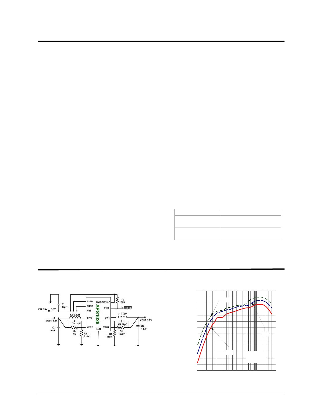
Typical Application
Figure 1. Basic Application Circuit
.
Analog Power Semiconductor Version_1.0 1/25/2006 1
APS1026 Efficiency vs Load Current
100
95
90
85
80
75
70
65
60
EFFICIENCY ( %)
55
50
45
40
35
0.1 1 10 100 1000
1.8V
1.2V
LOAD CURRENT (mA
TA = 25C
V
= 3.3V
IN
1.5V
Page 2
APSemi APS1026
+0.3V
IN
(Note 1)
Peak SW1, SW2 Sink & Source Current ..... 1.5A
Operating Temperature Range... -40°C to +85°C
Junction Temperature
(Note2)
.....................+125°C
Storage Temperature Range .... -65°C to +150°C
Lead Temperature (Soldering, 10s).........+300°C
Absolute Maximum Rating
Input Supply Voltage ...................... -0.3V to +6V
RUN1, RUN2........................... -0.3V to VIN+0.3V
VFB1, VFB2 Voltages ............. -0.3V to VIN+0.3V
SW1, SW2 Voltages................ -0.3V to V
POR Voltages ......................... -0.3V to VIN+0.3V
Package/Order Information
10-Lead (3mm X 3mm) Plastic DFN
Exposed Pad is PGND (Pin 11)
Must be connected to GND.
10-Lead Plastic MSOP
Exposed Pad is PGND (Pin 11)
Must be connected to GND.
Part Number Top Mark Temp Range Part Number Top Mark Temp Range
APS1026EDJ D2XY
(Note4)
-45℃ to 85℃
APS1026EMJ D1XY
Thermal Resistance
Package Ө
MSOP-10 (EXPOSE PAD)
DFN-10 (EXPOSE PAD)
Note 1: Absolute Maximum Ratings are those values beyond which the life of a device may be impaired.
Note 2: TJ is calculated from the ambient temperature T
T
Note 3: Thermal Resistance is specified with approximately 1 square of 1 oz copper.
Note 4: XY = Manufacturing Date Code. X = Year and Y = Week.
= TA + (PD) x Ө
J
JA
.
(Note 3)
:
JA
Ө
JC
45℃/W 10℃/W
45℃/W 10℃/W
and power dissipation PD according to the following formula:
A
-45℃ to 85℃
Analog Power Semiconductor Version_1.0 1/25/2006 2
Page 3
APSemi APS1026
Electrical Characteristics
(VIN =V
= 3.6V, TA = 25°C, Test circuit of Figure 3, unless otherwise noted.)
RUN
(Note 5)
Parameter Conditions MIN TYP MAX Unit
Input Voltage Range 2.5 5.5 V
Input DC Supply Current
Active Mode
Sleep Mode
Shutdown Mode
Regulated
Feedback Voltage
V
= V
= V
= 0.5V, MODE = GND
FB2
= 0.63V, MODE = 3.6V
FB2
FB1
V
FB1
RUN = 0V, VIN = 4.2V, MODE = 0V
500
45
0.3
TA = +25°C, Channel 1 or 2 0.5880 0.6000 0.6120 V
TA= 0°C TA 85°C, Channel 1 or 2 0.5865 0.6000 0.6135 V
T
= -40°C TA 85°C, Channel 1 or 2 0.5850 0.6000 0.6150 V
A
800
60
2
µA
µA
µA
Feedback Pin Input Current VFB = 0.65V ±30 nA
Reference Voltage Line
Regulation
Output Voltage Line
Regulation
Output Voltage Load
Regulation
= 2.5V to 5.5V, V
V
IN
VIN = 2.5V to 5.5V, V
I
= 10mA
OUT
= VFB (R2=0) 0.04 0.40 %/V
OUT
= 1.8V,
OUT
VIN = 3.6V, ,
I
= 0 to 600mA, Mode = 3.6V or 0V
OUT
0.24 0.40 %/V
0.0015 %/mA
Maximum Output Current V
Oscillator Frequency V
R
R
of P-CH MOSFET VIN = 3.6V, IL = 100mA 0.35 0.45
DS(ON)
of N-CH MOSFET VIN = 3.6V, IL = 100mA 0.28 0.45
DS(ON)
Peak Inductor Current VIN=3V, V
SW Leakage V
Output Over Voltage
Lockout
= 3.0V 600 mA
IN
= 0.6V 1.2 1.5 1.8 MHz
FB1/2
= V
FB1
= 0V, VSW= 0V or 5V, VIN = 5V ±0.01 ±1 µA
RUN
V
OVLX
= V
OVLX
= 0V, SW1 or SW2 1.0 A
FB2
– V
20 50 80 mV
FBX
RUN Threshold -40°C TA 85°C 0.3 0.45 1.30 V
RUN Leakage Current ±0.1 ±1 µA
V
Ramping Up, MODE/SYN = 0V 8.5 %
FBX
V
Ramping Down, MODE/SYN =
Power-On Reset Threshold
(POR)
FBX
0V
Power-On Reset Delay 175 mS
-8.5 %
Power-On Reset On-Resistance 100
Note 5: 100% production test at +25°C. Specifications over the temperature range are guaranteed by design and
characterization.
Analog Power Semiconductor Version_1.0 1/25/2006 3
Page 4
APSemi APS1026
)
)
)
)
)
)
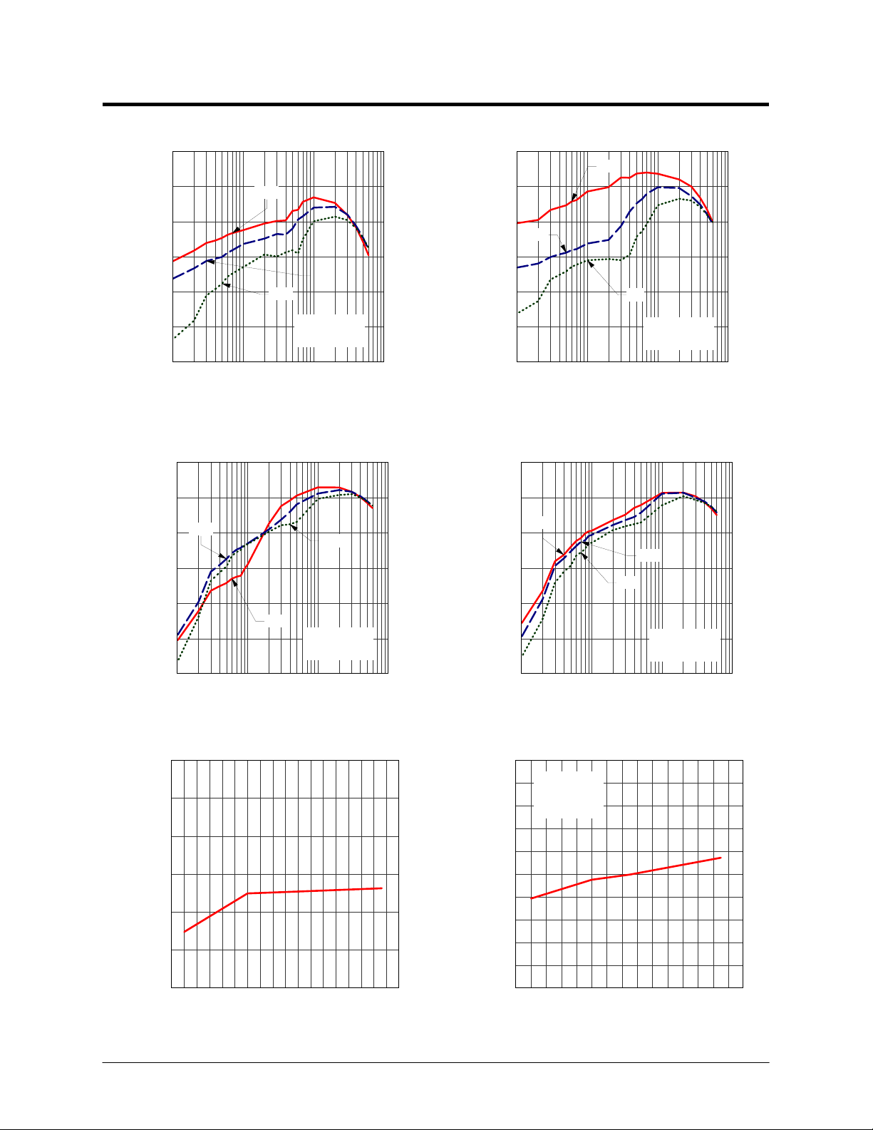
Typical Performance Characteristics
(Test Figure 1 above unless otherwise specified)
Efficiency vs Load Current
100
Power Saving Mode
90
80
70
60
50
40
EFFICIENCY (%)
30
20
10
0
0.1 1 10 100 1000
Oscillator Frequency vs Supply Voltage
1.8
1.7
Idle Mode
1.6
Pulse Skipping Mode
VIN = 3.6V
VOUT = 1.8V
TA = 25C
NO LOAD ON
OTHER CHANNEL
LOAD CURRENT (mA
L = 2.2μH
Iload = 150mA
Vout = 1.8V
Efficiency vs Input Voltage
100
95
90
85
80
1mA
75
EFFICIENCY (%)
70
TA = 25C
65
VOUT = 1.8V
60
2 3 4 56
4.0
TA = 25C
3.0
2.0
Pulse Skipping Mode
1.0
100mA
10mA
INPUT VOLT AGE (V
Load Regulation
Power Saving Mode
600mA
1.5
1.4
OSCILLATOR FREQUENCY (MHz)
1.3
1.2
2.7 3.15 3.6 4.05 4.5 4.95 5.4
Power Saving Mode
SUPPLY VOLTAGE (V
Power Saving Mode Operation
Efficiency vs Load Current
100
95
90
85
80
75
EFFICIENCY (%)
70
65
2.7V
3.3V
4.2V
TA = 25C
VOUT = 1.2V
0.0
ERROR (%)
OUT
-1.0
V
-2.0
VIN = 3.6V
VOUT = 1.8V
-3.0
NO LOAD ON OTHER CHANNEL
-4.0
1 10 100 1000
LOAD CURRENT (mA
Power Saving Mode Operation
Efficiency vs Load Current
100
95
90
85
80
75
EFFICIENCY (%)
70
65
2.7V
3.3V
4.2V
TA = 25C
VOUT = 1.5V
60
1 10 100 1000
LOAD CURRENT (mA
Note: No load on the other channel
60
1 10 100 1000
LOAD CURRENT (mA
Note: No load on the other channel
Analog Power Semiconductor Version_1.0 1/25/2006 4
Page 5
APSemi APS1026
)
)
)
)
)
)
Power Saving Mode Operation
Efficiency vs Load Current
100
95
2.7V
Power Saving Mode Operation
Efficiency vs Load Current
100
2.7V
95
90
85
EFFICIENCY
80
75
70
1 10 100 1000
LOAD CURRENT (mA
4.2V
3.3V
TA = 25C
VOUT = 1.8V
Note: No load on the other channel
Idle Mode Operation
Efficiency vs Load Current
100%
90%
3.3V
80%
70%
EFFICIENCY (%)
60%
2.7V
50%
40%
1 10 100 1000
LOAD CURRENT (mA
4.2V
TA = 25C
VOUT = 1.8V
Note: No load on the other channel
Oscillator Frequency vs Temperature
1.800
1.700
1.600
1.500
1.400
FREQUENCY (MHz)
1.300
1.200
-48 -32 -16 0 16 32 48 64 80 96
TEMPERATURE (C
90
3.3V
85
EFFICIENCY (%)
80
75
70
1 10 100 1000
LOAD CURRENT (mA
4.2
TA = 25C
VOUT = 2.5V
Note: No load on the other channel
Idle Mode Operation
Efficiency vs Load Current
100%
90%
2.7V
80%
4.2V
3.3V
TA = 25C
VOUT = 1.5V
70%
EFFICIENCY (%)
60%
50%
40%
1 10 100 1000
LOAD CURRENT (mA
Note: No load on the other channel
VFB vs Temperature
0.612
0.610
0.608
0.605
0.602
0.600
0.598
VOLTAGE (C)
0.595
0.592
0.590
0.588
Vin = 3.6V
Vout = 1.8V
Iload = 0mA
-50 -30 -10 10 30 50 70 90
TEMPERATURE (C
Analog Power Semiconductor Version_1.0 1/25/2006 5
Page 6

APSemi APS1026
)
Rds(on) vs Input Voltage
0.4
0.38
0.36
0.34
0.32
0.3
0.28
RDS(ON) (Ω)
0.26
0.24
0.22
0.2
2 2.4 2.8 3.2 3.6 4 4.4 4.8 5.2 5.6 6
Synchr onous Switc h
INPUT VOLT AGE (V
TA = 25C
Main Switch
Load Transient Response
Power Saving Mode to PWM mode
Load Transient Response
PWM Mode Only
Load Transient Response
Idle Mode to PWM mode
Analog Power Semiconductor Version_1.0 1/25/2006 6
Page 7

APSemi APS1026
Pin Description
PIN NAME FUNCTION & Description
1 VFB1
2 RUN1 Channel 1 Enable
3 VIN Power Supply
4 SW1 Channel 1 power switch output
5 GND Ground
6 MODE/SYNC
7 SW2 Channel 2 power switch output.
8 POR Power On Reset.
9 RUN2 Enable pin of Channel 2.
10 VFB2
11 EXPOSED PAD Power Ground. It must be connect to ground properly.
Functional Block Diagram
Channel 1 output feedback. It receives the feedback voltage from the external
resistive divider across the output.
Combination Mode selection and Oscillator Synchronization.
When MODE/SYNC = High, the circuit is in Idle mode operation;
When MODE/SYNC = High, the circuit is in power saving mode operation.
Channel 2 output feedback.
resistive divider across the output.
It receives the feedback voltage from the external
Figure 2. APS1026 Block Diagram
Analog Power Semiconductor Version_1.0 1/25/2006 7
Page 8

APSemi APS1026
Operation
The APS1026 is a monolithic switching mode
Step-Down DC-DC converter. It utilizes internal
MOSEFETs to achieve high efficiency and can
generate very low output voltage by using
internal reference at 0.6V. It operates at a fixed
switching frequency, and uses the slope
compensated current mode architecture. This
Step-Down DC-DC Converter supplies 600mA
output current at VIN = 3V with input voltage
range from 2.5V to 5.5V. With the mode
selection pin, users may select the Power
Saving Mode, optimizing efficiency at light load
(Mode=Vin) or the Idle Mode, optimizing ripple at
light load (Mode=GND).
Current Mode PWM Control
Slope compensated current mode PWM control
provides stable switching and cycle-by-cycle
current limit for excellent load and line
responses and protection of the internal main
switch (P-Ch MOSFET) and synchronous
rectifier (N-CH MOSFET). During normal
operation, the internal P-Ch MOSFET is turned
on for a certain time to ramp the inductor current
at each rising edge of the internal oscillator, and
switched off when the peak inductor current is
above the error voltage. The current
comparator, I
current. When the main switch is off, the
synchronous rectifier will be turned on
immediately and stay on until either the inductor
current starts to reverse, as indicated by the
current reversal comparator, I
beginning of the next clock cycle. The OVDET
comparator controls output transient overshoots
by turning the main switch off and keeping it off
until the fault is no longer present.
limits the peak inductor
COMP,
, or the
ZERO
Idle Operation
Two modes, the power saving mode and idle
mode, are available to control the operation of
the APS1026 at low currents. Both modes
automatically switch from continuous operation
to the selected mode when the load current is
low.
The APS1026 may be selected to enter Idle
operation (Mode=Vin) at light load. In the pulsing
skipping mode, the inductor current may reach
zero or reverse on each pulse. The PWM control
loop will automatically skip pulses to maintain
output regulation. The bottom MOSFET is
turned off by the current reversal comparator,
and the switch voltage will ring. This is
I
ZERO,
discontinuous mode operation, and is normal
behavior for the switching regulator.
Power Saving Operation
The APS1026 may be selected to enter Power
Saving Mode (Mode=GND) at light load. In
power saving mode at light load, a control circuit
puts most of the circuit into sleep in order to
reduce quiescent current and improve efficiency
at light load. When the output voltage drops to
certain threshold, the control circuit turns back
on the oscillator and the PWM control loop,
boosting output backup. When an upper
threshold is reached, the control circuit again
puts most of circuit into sleep, reducing
quiescent current. While the power saving
mode improves light load efficiency, however,
with the turning on and off, the noise or ripple
voltage is larger than that in the pulse skiing
mode.
Dropout Operation
When the input voltage decreases toward the
value of the output voltage, the APS1026 allows
the main switch to remain on for more than one
switching cycle and increases the duty cycle
until it reaches 100%. The duty cycle D of a
step-down converter is defined as:
V
fTD
OSCON
Where T
oscillator frequency.
The output voltage then is the input voltage
minus the voltage drop across the main switch
and the inductor. At low input supply voltage,
the R
increases, and the efficiency of the converter
decreases. Caution must be exercised to
ensure the heat dissipated not to exceed the
maximum junction temperature of the IC.
is the main switch on time and f
ON
DS(ON)
of the P-Channel MOSFET
V
OUT
IN
OSC
%100%100 ×≈××=
is the
Maximum Load Current
The APS1026 will operate with input supply
voltage as low as 2.5V, however, the maximum
load current decreases at lower input due to
large IR drop on the main switch and
synchronous rectifier. The slope compensation
Analog Power Semiconductor Version_1.0 1/25/2006 8
Page 9

APSemi APS1026
signal reduces the peak inductor current as a
function of the duty cycle to prevent subharmonic oscillations at duty cycles greater than
50%. Conversely the current limit increases as
the duty cycle decreases.
Layout Guidance
When laying out the PC board, the following
suggestions should be taken to ensure proper
operation of the APS1026. These items are also
illustrated graphically in Figure 3 and 4.
1. The power traces, including the GND trace,
the SW trace and the VIN trace should be
kept short, direct and wide.
2. The VFB pin should be connected directly to
the feedback resistor. The resistive divider
R1/R2 must be connected between the (+)
plate of COUT and ground.
3. Connect the (+) plate of CIN to the VIN pin
as closely as possible. This capacitor
provides the AC current to internal power
MOSFET.
4. Keep the switching node, SW, away from
the sensitive VFB node.
5. Keep the (-) plates of CIN and COUT as
close as possible.
Figure 3. APS1026 Typical Application Circuit
Figure 4. APS1026 Typical Application Circuit Layout
Analog Power Semiconductor Version_1.0 1/25/2006 9
Page 10

APSemi APS1026
APPLICATIONS
INFORMATION
Setting the Output Voltage
Figure 3 above shows the basic application
circuit for the APS1026. The external resistor
sets the output voltage according to the
following equation:
R
⎛
VV
OUT
Table 1 – Resistor select for output voltage
setting
V
OUT
1.2V 316k 316k
1.5V 316k 474k
1.8V 316k 632k
2.5V 316k 1001k
⎜
⎝
R1(R3) R2(R4)
Inductor Selection
For most designs, the APS1026 operates with
inductors of 1µH to 4.7µH. Low inductance
values are physically smaller but require faster
switching, which results in some efficiency loss.
The inductor value can be derived from the
following equation:
()
=
IΔ
=210mA.
L
L
IΔ
L
Where is inductor Ripple Current. Large
value inductors lower ripple current and small
value inductors result in high ripple currents.
Choose inductor ripple current approximately
35% of the maximum load current 600mA, or
For output voltages above 2.0V, when light-load
efficiency is important, the minimum
recommended inductor is 2.2µH. For optimum
voltage-positioning load transients, choose an
inductor with DC series resistance in the 50m
to 150m range. For higher efficiency at heavy
loads (above 200mA), or minimal load regulation
(but some transient overshoot), the resistance
should be kept below 100m. The DC current
2
16.0
⎞
+=
⎟
R
1
⎠
−×
VVV
OUTINOUT
×Δ×
fIV
OSCLIN
rating of the inductor should be at least equal to
the maximum load current plus half the ripple
current to prevent core saturation
(600mA+105mA). Table 1 lists some typical
surface mount inductors that meet target
applications for the APS1026.
Part #
Sumida
CR43
Sumida
CDRH4D18
Toko
D312C
L
(µH)
1.4
2.2
3.3
4.7
1.5
2.2
3.3
4.7
1.5
2.2
3.3
4.7
Max
DCR
(m)
56.2
71.2
86.2
108.7
75
110
162
120
140
180
240
Rated
D.C.
Current
(A)
2.52
1.75
1.44
1.15
1.32
1.04
0.84
1.29
1.14
0.98
0.79
Size
WxLxH
(mm)
4.5x4.0x3.5
4.7x4.7x2.0
3.6x3.6x1.2
Input Capacitor Selection
The input capacitor reduces the surge current
drawn from the input and switching noise from
the device. The input capacitor impedance at
the switching frequency shall be less than input
source impedance to prevent high frequency
switching current passing to the input. A low
ESR input capacitor sized for maximum RMS
current must be used. Ceramic capacitors with
X5R or X7R dielectrics are highly recommended
because of their low ESR and small temperature
coefficients. A 4.7µF ceramic capacitor for most
applications is sufficient.
Output Capacitor Selection
The output capacitor is required to keep the
output voltage ripple small and to ensure
regulation loop stability. The output capacitor
must have low impedance at the switching
frequency. Ceramic capacitors with X5R or X7R
dielectrics are recommended due to their low
ESR and high ripple current. The output ripple
is determined by:
V
OUT
Analog Power Semiconductor Version_1.0 1/25/2006 10
Page 11

APSemi APS1026
Package Description
MSOP-10
Figure 5 Package Dimensions of 10-lead Plastic MSOP
Analog Power Semiconductor Version_1.0 1/25/2006 11
Page 12

APSemi APS1026
DFN-10
Dimension: mm
A 0.75
A1 0.02
A3 0.20 ref
aaa 0.15
bbb 0.10
ccc 0.10
ddd 0.05
eee 0.08
ggg 0.10
D BSC 3.00
E BSC 3.00
D2 2.20-2.70
E2 1.40-1.75
L 0.40
N 10
ND 5
Figure 6 Package Dimensions of 10-lead Plastic DFN (3mmX3mm)
Analog Power Semiconductor Version_1.0 1/25/2006 12
Page 13

APSemi APS1026
IMPORTANT NOTICE
Analog Power Semiconductor (ShangHai) Co., Ltd. reserves the right to make changes without further
notice to any products or specifications herein. Analog Power Semiconductor (ShangHai) Co., Ltd. does
not assume any responsibility for use of any its products for any particular purpose, nor does Analog
Power Semiconductor (ShangHai) Co., Ltd assume any liability arising out of the application or use of any
its products or circuits. Analog Power Semiconductor (ShangHai) Co., Ltd does not convey any license
under its patent rights or other rights nor the rights of others.
Analog Power Semiconductor
IPCore Technologies (Shanghai) Co., Ltd.
11 Floor, Block B, Hi-Tech Building, 900 Yishan Road,
Shanghai, 200233, P.R. China
Tel: (8621) 5423-5088
Fax: (8621) 5423-5090
http://www.apsemi.com; http://www.ipcoreinc.com
Analog Power Semiconductor Version_1.0 1/25/2006 13
Page 14

 Loading...