

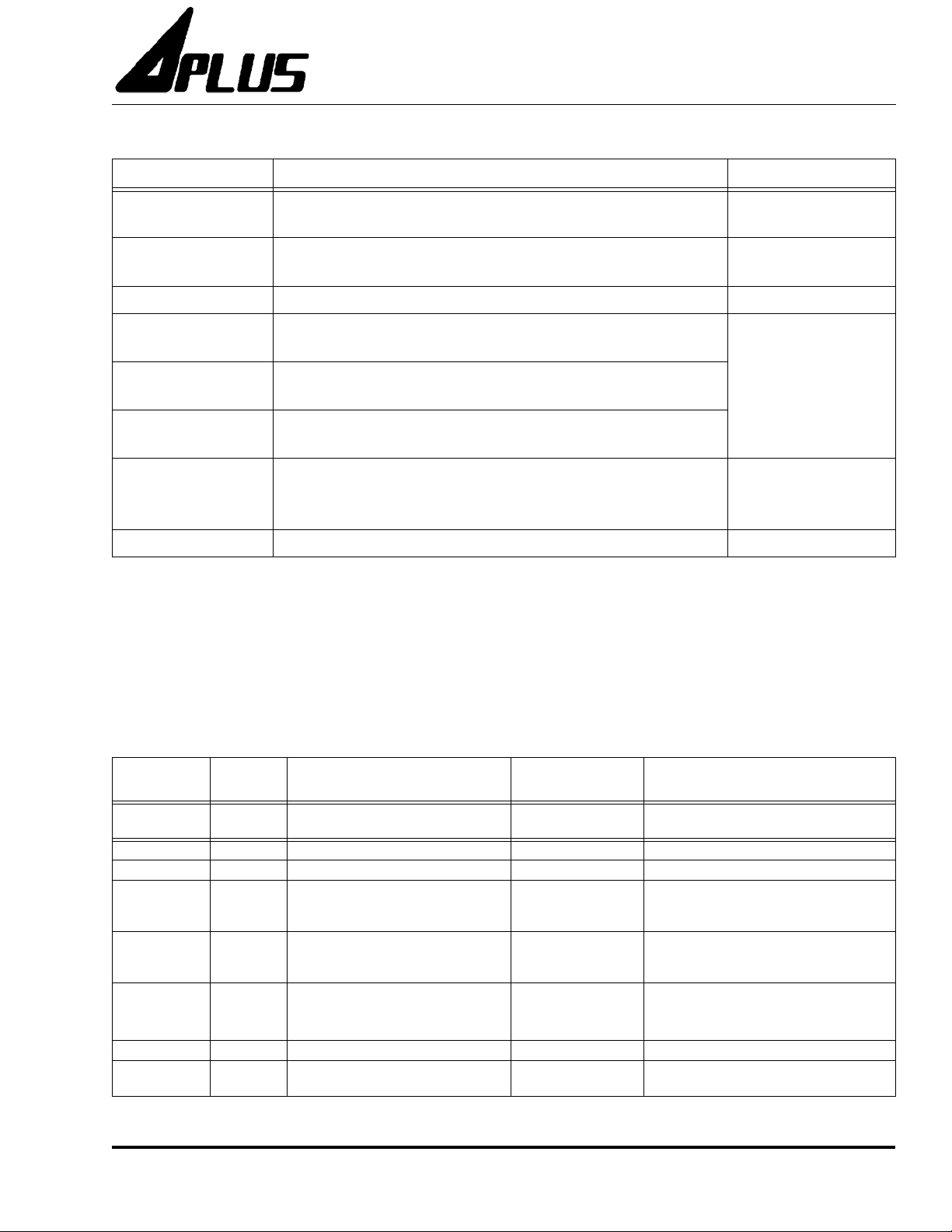
Page 1
INTEGRATED CIRCUITS INC.
APR6008
Voice Recording & Playback Device
8 Minute Duration
Features
•Multi-level analog storage
-High quality audio recording and playback
•Dual mode storage of analog and/or digital data
-Eliminates the need for separate digital memory
•Advanced, non-volatile Flash memory technology
-No battery backup required
•SPI interface
-Allows any commercial microcontroller to control
the device
•Programmable Sampling Clock
-Allows user to choose quality and duration levels
•Single 3V power supply
•Low power consumption
-Playback operating current: 15 mA typical
-Standby current: 1 uA maximum
-Automatic power-down
•Multiple package options available
-CSP, SOP, PDIP, Bare Die
•On-board clock prescaler
-Eliminates the need for external clock dividers
•Automatic squelch circuit
Reduces background noise during quiet passages
-
General Description
Figure 1 APR6008 Pinout Diagrams
The APR6008 offers non-volatile storage of voice and/or data
in advanced Multi-Level Flash memory. Up to 8 minutes of
audio recordin
imum of 30K bits of di
devices can be cascaded for lon
greater digital storage. Device control is accomplished
throu
gh an industry standard SPI interface that allows a
microcontroller to mana
This flexible arran
messa
ging options. The APR6008 is ideal for use in cellular
and cordless phones, telephone answerin
di
gital assistants, personal voice recorders, and voice pag-
ers.
APLUS Integrated
lity
by usin
i mplemented in an advanced non-volatile Flash memory
logy
process. Each memory cell can typically store 256 volta
levels. This allows the
si
gnals in their natural form, eliminating the need for en
ding
and compression which can introduce distortion.
2002/5/10 Page 1
g and playback can be accommodated. A max-
gital data can be stored.
APR6008
ger duration recording or
ge message recording and playback.
gement allows for the widest variety of
g devices, personal
achieves this high level of storage capabi-
g a proprietary analog multi-level storage te
APR6008 voice
to
reproduce audio
chno
co-
ge
28 pin DIP
/CS
1
DI
2
DO
NC
NC
NC
NC
3
4
5
6
7
8
9
10
11
12
13
14
VSSD
ANAOUT-
ANAOUT+
/RESET
l -
VSSA
AUDOUT
SQLCAP
28
27
26
25
24
23
22
21
20
19
18
17
16
15
SCLK
VCCD
EXTCLK
/INT
SAC
VSSA
NC
/BUSY
NC
NC
VCCA
ANAIN+
ANAIN/SQLOUT
Page 2
APR6008
Functional Description
The EXTCLK pin allows the use of an external sampling
clock. This input can accept a wide range of frequencies
dependin
that follows the clock. Alternativel
nal oscillator can be used to suppl
Mux followin
si
gnal if a clock is present, otherwise the internal oscillator
source is chosen. Detailed information on how to pro
divider and internal oscillator can be found in the explanation
of the
Command Description
the appropriate sample clock fre
Sampling Rate & Voice Quality
The audio si
should be fed into the differential inputs ANAIN-, and
ANAIN+. After pre-amplification the si
anti-aliasin
its response based on the sample rate bein
nal anti-aliasin
After passin
the sample and hold circuit which works in con
the Analo
flash memor
g on the divider ratio programmed into the divider
y, the programmable inter-
y the sampling clock. The
g both signals automatically selects the EXTCLK
gram the
PWRUP
command, which appears in the
section. Guidance on how to choose
quency can be found in the
section.
gnal containing the content you wish to record
gnal is routed into the
g filter. The anti-aliasing filter automatically adapts
g used. No exter-
g filter is therefore required.
g through the anti-alias filter, the signal is fed into
g Write Circuit to store each analog sample in a
y cell.
OpCode
junction with
When a read operation is desired the Analog Read Circuit
extracts the analo
the si
gnal to the Internal Low Pass Filter. The low pass filter
converts the individual samples into a continuous output. The
output si
fferential output driver. The differential output driver feeds the
ANAOUT+ and ANAOUT- pins. Both differential output pins
swin
The s
si
control si
reducin
mation, refer to the
After passin
goes to the output amplifier. The output amplifier drives a single ended output on the AUDOUT pin. The single ended output swin
All SPI control and hand shakin
Master Control Circuit. This circuit decodes all the SPI si
and
the status re
the APR6008 .
gnal then goes to the squelch control circuit and di-
g around a 1.23V potential.
quelch control circuit automatically reduces the output
gnal by 6 dB during quiet passages. A copy of the squelch
gnal is present on the SQLOUT pin to facilitate
g gain in the external amplifier as well. For more infor-
gs around a 1.23V potential.
generates all the internal control signals. It also contains
g data from the memory array and feeds
Squelch
g through the squelch circuit the output signal
gister used for examining the current status of
section.
g signals are routed to the
gnals
Figure 2 APR6008 Block Diagram
/RESET
/BUSY
SAC
/INT
DO
DI
/CS
SCLK
EXTCLK
Row
Address
Row Decoder
Master Control Circuit
Column Address
Programmable Internal
Oscillator
Programmable
Divider
1.92 Mcell Memory Array
Single Analog
Memory Cell
Column Decoder
Analog input/output
to Memory array
Mux
Low Pass
Write Circuit
Read Circuit
Low Pass
Squelch
Pre-
Amp
Amp
Amp
ANAIN+
ANAIN-
ANAOUT+
ANAOUT-
AUDOUT
SQLCAP
/SQLOUT
Page 2 Voice Recording & Playback Device
Revision 2.1
Page 3
APR6008
Memory Organization
The APR6008 memory array is organized to allow the greatest flexibilit
The smallest addressable memor
The APR6008 contains 640 sectors.
y in message management and digital storage.
y unit is called a “sector”.
Figure 3 Memory Map.
SAC Trigger Point
Sector 0
Sector 1
Sector 639
Sectors 0 through 639 can be used for analog storage. Du ring
audio recording one memory cell is used per sample
clock c
ycle. When recording is stopped an end of data (EOD)
bit is programed into the memory. This prevents playback of
silence when partial sectors are used. Unused memor
exists between the EOD bit and the end of the sector can not
be used.
Sectors 0 throu
stora
ge. Other sectors, with the exception of sector 639, can
store data but have not been tested, and are thus not
teed to provide 100%
error correction or forward check-before-store methods.
Once a write c
chosen sector is lost.
Mixin
g audio signals and digital data within the same sector is
not possible.
Note: There are a total of 15bits reserved for addressing. The
APR6008 only
for larger devices within the APR6008 family.
Can Not be Used for Digital Data
y that
gh 9 are tested and guaranteed for digital
guaran-
good bits. This can be managed with
ycle is initiated all previously written data in the
requires 10 bits. The additional 5 bits are used
SPI Interface
All memory management is handled by an external host processor. The host processor communicates with the APR6008
throu
gh a simple Serial Peripheral Interface (SPI) Port. The
SPI port can run on as little as three wires or as man
seven dependin
section will describe how to mana
APR6008 SPI Port and associated OpCode commands.
This topic is broken down into the followin
•Sendin
•OpCode Command Description
•Receivin
•Current Device Status
•Reading the Silicon Identification (SID)
•Writin
•Readin
•Recordin
•Pla
•Handshakin
Sending Commands to the Device
This section describes the process of sendin
the APR6008 All Opcodes are sent in the same wa
exception of the
The
in the
that follow. The minimum SPI confi
commands uses the DI, /CS, and SCLK pins. The device will
accept inputs on the DI pin whenever the /CS pin is low.
OpCode commands are clocked in on the risin
SPI clock. Fi
OpCode commands into the device. Figure 5 is a description
of the OpCode stream.
You must wait for a command to finish executin
in
BUSY pin. You can substitute monitorin
inserting a fixed delay between commands. The required
dela
shows the timin
mands. Table 1 describes which
g Digital Data
ying Back Audio Data
DIG_WRITE and DIG_READ
Writing Digital Data
g a new command. This is accomplished by monitoring the /
y is specified as
g on the amount of control necessary. This
ge memory using the
g sections:
g Commands to the Device
g Device Information
(CDS)
g Digital Data
g Audio Data
g Signals
g OpCodes to
DIG_WRITE
and
gure 4 shows the timing diagram for shifting
T
g diagram for sending consecutive com-
next1,Tnext2,Tnext3
DIG_READ
and
commands
are
Reading Digital Data
guration needed to send
g edge of the
g before send-
g of the busy pin by
or T
next4
specification to use.
T
next
y as
y with the
commands
described
sections
. Figure 6
.
Voice Recording & Playback Device Page 3
Revision 2.1
Page 4
APR6008
Figure 4Sending SPI Commands
/CS
SCLK
~
~
T
hiSCLK
~
~
T
next1
, T
~
~
next2
~
~
, T
next3
, T
next4
T
fCS
DI
Figure 5OpCode Format
Op4Op3 Op1Op0A14A13A12A11A10 A9 A8 A7 A6Op2
Op4
First bit shifted in
Op3
Op2 Op1
T
suDI
T
pSCLK
{
OpCode Command OpCode Parameter
Figure 6Opcode Stream Timing
A0
A0
T
rCS
~
~
T
loSCLK
~
~
T
A5 A4 A3 A2 A1
A1A2
hDI
Last bit shifted in
{
SCLK
/CS
DI
Page 4 Voice Recording & Playback Device
Current Command Next Command
T
next1,Tnext2,Tnext3,Tnext4
Revision 2.1
Page 5
APR6008
Table 1 Sequential Command Timing
Current Command Next command Timing Symbol
NOP
Any Command T
SID
PWRUP
Any Command T
STOP_PWDN PWRUP
SET_REC
STOP, STOP_PWDN, SET_REC, REC,NOP
REC
SET_PLAY
STOP, STOP_PWDN, SET_FWD, FWD, SET_PLAY,PLAY, NOP
PLAY
SET_FWD
SET_FWD, FWD, STOP, STOP_PWDN
FWD
DIG_WRITE
DIG_READ
DIG_ERASE
STOP
Any Digital Command,
Note: For partial DIG_READ T
rise of /CS, not from the rise of /CS
Any Command T
STOP, STOP_PWDN
is measured from the extra clock low that follows the 8K sampling rate: 376m SEC
next2
OpCode Command Description
Designers have access to a total of 14 OpCodes. These
OpCodes are listed in Table 2. The name of the Opcode
appears in the left hand column. The followin
represent the actual binar
y information contained in the 20 bit
data stream. Some commands have limits on which com-
g two columns
next1 5u SEC
next2 5m SEC
T
next2 5m SEC
Within SAC Low Time
T
next3
4K sampling rate: 752 m SEC
next4 470m SEC
mand can follow them. These limits are shown in the “
able Follow on Commands
” column. The last column
Allow-
summarizes each command.
Combinations of OpCodes can be used to accommodate
almost an
y memory management scheme.
Table 2
Instruction
Name
NOP
SID
SET_FWD
FWD
PWRUP
STOP
STOP_PWDN
Voice Recording & Playback Device Page 5
Revision 2.1
Operational Codes
APR6008
OpCode
(5 bits) Opcode Parameters (15bits)
[Op4 - Op0]
[00000] [Don’t Care] All Commands No Operation
[00001] [Don’t care] All Commands Causes the silicon ID to be read.
[00010] Sector Address
[00011] [Don’t care] SET_FWD,
[00100] [A14-A10]: all zeros
[00110] [Don’t care] All Commands Stops the current operation.
[00111] [Don’t care] PWRUP Stops the current operation. Causes the
[Address MSB - Address LSB]
[Address 14 - Address 0]
[A14 - A0]
[A9-A2]: EXTCLK divider ratio
[A1-A0]: Sample Rate Frequency
Allowable Follow
on Commands Summary
SET_FWD,
FWD, STOP,
STOP_PWDN
FWD, STOP,
STOP_PWDN
All Commands Resets the device to initial conditions.
Starts a fast forward operation from the
sector address specified.
Starts a fast forward operation from the
current sector address.
Sets the sample frequency and divider
ratios.
device to enter power down mode.
Page 6
APR6008
Instruction
Name
SET_REC
REC
DIG_ERASE
DIG_WRITE
DIG_READ
SET_PLAY
PLAY
OpCode
(5 bits) Opcode Parameters (15bits)
[Op4 - Op0]
[01000] Sector Address
[01001] [Don’t care] STOP,
[01010] Sector Address
[01011] [A14 - A0][XXXX][D0 - D3004][XXXX] All Commands This command writes data bits D0 - D3003
[01111] Sector A d dress
[01100] Sector Address
[01101] [Don’t care] STOP,
[Address MSB - Address LSB]
[Address 14 - Address 0]
[A14 - A0]
[A14 - A0]
[A14 - A0]
[A14 - A0]
Allowable Follow
on Commands Summary
STOP,
STOP_PWDN,
SET_REC,
REC,NOP
STOP_PWDN,
SET_REC,
REC,NOP
All Commands Erases all data contained in specified sec-
All Commands This command reads data bits D0 - D3003
STOP,
STOP_PWDN,
SET_FWD, FWD,
SET_PLAY,PLAY,
NOP
STOP_PWDN,
SET_FWD, FWD,
SET_PLAY,PLAY,
NOP
Starts a record operation from the sector
address specified.
Starts a record operation from the current
sector address.
tor. You must not erase a sector before
recording voice signals into it. You must
erase a sector before storing digital data in
it.
starting at the specified address. All 3004
bits must be written.
starting at the specified address.
Starts a play operation from the sector
address specified.
Starts a play operation from the current
sector address.
NOP
The
command performs no operation in the device. It is
most often used when readin
more information on readin
Device Status
SID
THE
of its silicon ID re
ing the SID
SET_FWD
The
from the be
section.
operation instructs the device to return the contents
gister. For more information see the
section.
command instructs the device to fast forward
ginning of the sector specified in the OpCode
g the current device status. For
g device status see the
Current
Read-
The device will continue to fast forward in this manner until
either an EOD is reached, a new command is sent, or the end
of the memor
the device will stop and
The output amplifiers are muted durin
PWRUP
The
mode and set the internal clock fre
divider ratio. To select an Internal oscillator fre
[A1 - A0] bits accordin
y array is reached. When an EOD is reached
generate an interrupt on the /INT pin.
g this operation.
command causes the device to enter power up
quency and EXTCLK
quency set the
g to the following binary values:
parameter field. The device will fast forward until either an
EOD bit, or the end of the sector is reached. If no EOD bit or
forthcomin
the sector is reached, the device will loop back to the be
nin
an EOD bit is found the device will stop and
g command has been received when the end of
gin-
g of the same sector and begin the same process again. If
generate an
interrupt on the /INT pin. The output amplifiers are muted durin
g this operation.
FWD
The
command instructs the device to fast forward from
the start of the current sector to the next EOD marker. If no
EOD marker is found within the current sector the device will
increment to the next se
Page 6 Voice Recording & Playback Device
quential sector and continue looking.
A1 A0 Sample rate
0 0 6.4 kHz
0 1 4.0 kHz
1 0 8.0 kHz
1 1 5.3 kHz
If
you are using an external sample clock signal you must
also set the EXTCLK divider ratio. This divider ratio is e
to N:1 where N is an inte
The N value should be selected to satisf
ger between 1 and 256, excluding 2.
y the following equa-
Revision 2.1
qual
Page 7

APR6008
tion as closely as possible:
EXTCLK fre
Example:
Suppose that 8.0 KHz samplin
the fre
N
Roundin
The Op Code Parameter bit stream, composed of bits
[A9 - A2][A1 - A0], therefore becomes binar
[00001000][10].
STOP
The
operation.
STOP_PWDN
The
current command and enter power down mode. Durin
down the device consumes si
PWRUP command must be used to force the device into
power up mode before an
SET_REC
The
recordin
continue to record until the end of the current sector is
reached. If no forthcomin
when the end of the sector is reached the device will loop
back to the be
previousl
SET_REC
mand immediatel
that no audio information is lost. For more information see the
section entitled
REC
The
the current sector. If no new command is received before the
device reaches the end of the sector the device will automaticall
y increment to the next sequential sector and continue
recordin
until the memor
command is received. For more information see the section
entitled
DIG_ERASE
The
sector specified. Erase should not be done before recordin
voice signals into a sector. Erase must be done before storing
digital data in a sector.
DIG_WRITE
The
the specified sector. All 3K bits must be written, no partial
usa
ge of the sector is possible. The memory acts as a FIFO,
the first data bit shifted in will be the first data bit shifted out. A
sector must be erased usin
BEFORE
tion on storin
Digital Data
DIG_READ
The
q = (N) * (128) * (selected sampling frequency)
g is desired. Assume that
quency of the signal present on EXTCLK = 8MHz.
8000000
-------------------------1288000()
g up, N = 8
Command causes the device to stop the current
g at the sector address specified. The device will
y recorded material. If the next command is another
REC
or
command instructs the device to begin recording in
g. The device will continue to record in this manner
Recording Audio Data
data can be written to the sector. For more informa-
g digital data, see the section entitled
.
7.8125==
command causes the device to stop the
g power
gnificantly less power. The
y commands can be executed.
command instructs the device to begin
g command has been received
ginning of the same sector and overwrite the
command the device will execute the com-
y following the end of the current sector so
Recording Audio Data
y is exhausted or a
.
command erases all data contained in the
command stores 3K bits of digital data in
g the
.
STOP
STOP_PWDN
or
DIG_ERASE
command
Writing
command instructs the device to retrieve
di
gital data that was previously written to the specified sector.
The first bit shifted out is the first bit that was written. The last
bit shifted out is the last bit that was written. For more information on readin
g digital data see the section entitled
ing Digital Data.
SET_PLAY
The
back at the specified sector. If no forthcomin
received, or EOD bit encountered, before the end of the sector is reached the device will loop back to the be
same sector and continue pla
the audio output. If the next command is another
PLAY
or
immediatel
y
gap in playback is present. For more information see the section entitled
PLAY
The
the current sector. If no forthcomin
EOD bit encountered, before the device reaches the end of
the sector the device will automaticall
se
quential sector and continue playing. The device will con-
tinue to pla
STOP
a
information see the section entitled
g
or
command instructs the device to begin play-
g command is
ginning of the
yback with no noticeable gap in
command the device will execute the command
y following the end of the current sector so that no
Playing Back Audio Data.
command instructs the device to begin playback at
y in this manner until the memory is exhausted or
STOP_PWDN
command is received. For more
g command is received, or
y increment to the next
Playing Back Audio Data.
Read-
SET_PLAY
Voice Recording & Playback Device Page 7
Revision 2.1
Page 8

APR6008
Receiving Device Information
The device communicates data to the user by shifting out
data on the DO pin. The device will shift out data accordin
the timin
Figure 7 Data Out Timing
g parameters given in figure 7. The device can shift
/CS
SCLK
DI
DO
Op4
D0
Op3
Op2 Op1
D1 D2 D18 D17 D19 D16
D3
g to
~
~
~
~
~
~
~
~
out three different types of data streams: Device status, Silicon ID, and user stored data. Device status and silicon ID are
described in the next two sections. Retrieval of user data is
described in the
A3
D15
Reading Digital Data
A2
A1
section.
A0
T
fcsDO
Current Device Status (CDS)
As described in the previous section, three different types of
data streams are shifted out on the DO pin as data is shifted
in on the DI pin. One of these steams is the current device
status. The CDS will be shifted out unless the previous command is SID command. Fi
CDS bit stream. The first bit shifted out, D0, is the Overflow
fla
g. The Overflow flag is set to a binary 1 if an attempt was
made to record be
fla
g is set to a 0 if an overflow has not occurred. This flag is
Figure 8Format for CDS Bit Stream
Sector
yond the available memory. The Overflow
~
D19
T
fSCLK
gure 8 shows the format of the
}
~
Sector Address
ress
Sector Add
T
hzD0
cleared after it has been read. The D1 bit is the End of Data
g. The EOD flag is set when the device stops playing, or
fla
fast forwardin
fla
g is cleared after it has been read. The D2 bit is the Illegal
Address fla
gal address is sent to the device. The D3 bit is the Lbat flag.
This fla
below specification. The D4 bit is not used and should be
i
gnored. The last fifteen bits represent the address of the cur-
rent or last active sector.
g as a result of an EOD bit in memory. The EOD
g. The Illegal Address flag is set whenever an ille-
g is set when the device senses a supply voltage
First bit shifted outLast bit shifted out
D0 D1 D3 D4 D5 D6 D7 D8 D9 D10 D11 D12 D13 D14 D2
OVF
EOD
gal Address
Addre
LSB
ss MSB
Ille
Lbat
Page 8 Voice Recording & Playback Device
Revision 2.1
Page 9

APR6008
Reading the SID
Each device in the APR60XX series family contains an
embedded Silicon Identification
b
y the host processor to identify which family / family member
is bein
g used. Reading the device SID requires issuing two
Figure 9SID Timing
SCLK
/CS
DI
DO
SID Command Next Command
CDS Output Data
(SID). The SID can be read
OpCode commands; a SID command followed b
command, usuall
the SID data out on the DO pin as the command that follows
the SID command is clocked in. Fi
describes the process necessar
y a NOP command. The device will clock
gure 9 is a diagram that
y for reading SID information.
SID Output Data
y any other
The SID information follows the format given in Figure 10.
The first bit shifted out, D0, is the Overflow bit. The Overflow
bit is set to a binar
be
yond the available memory. The Overflow bit is set to a 0 if
an overflow has not occurred. This bit is cleared after it has
been read. The D1 bit is the End Of Data
bit is set when the device stops pla
a result of EOD bit in memor
has been read. The D2 bit is the Ille
gal Address Bit is set whenever an illegal address is sent to
Figure 10SID Bit Stream
D19
}
Ignore These
Bits
y 1 if an attempt was made to record
(EOD) bit. The EOD
ying or fast forwarding as
y. The EOD bit is cleared after it
gal Address Bit. The Ille-
~
~
}
Device
Code
10
0
}
APR6008 Device
Code (Binary)
0
the device. The D3 bit is the Lbat bit. This bit is set when the
device senses a suppl
lowin
g five bits represent the product family. The APR60XX
product famil
The next four bits represent the device code. The APR6008
device code is binar
seven bits are random data and should be i
y code is binary 01000 as shown in Figure 10.
}
Product
Famil
y
1
000
}
APR60XX Series
Famil
y (Binary)
y voltage below specification. The fol-
y 0100 as shown in Figure 10 The last
gnored.
First bit shifted outLast bit shifted out
D0D1D3D4D5D6D7D8D9D10D11D12D13D14 D2
OVF
EOD
gal Address
Ille
0
Lbat
Voice Recording & Playback Device Page 9
Revision 2.1
Page 10

g
g
g
g
g
g
g
g
y
y
g
g
g
g
g
y by
y
y
y
g
y
y
y
y
g
g
y
APR6008
Writing Digital Data
Digital data is written into the device using the
command. No mixing of analog data and digital data within a
sector is possible. Sectors 0 throu
anteed for di
ital storage. Other sectors, with the exception of
h 9 are tested and guar-
sector 639, can store data but have not been tested, and are
thus not
mana
methods. Issuin
cause data throu
A sector must be erased, usin
before di
necessar
uaranteed to provide 100% good bits. This can be
ed with error correction or forward check-before-store
DIG_ERASE
a
command on sector 639 will
hout all sectors to be lost.
DIG_ERASE
the
ital data can be written to it. This requirement is
whether analog data or digital data was previousl
stored in the sector. A sector should not be erased more than
once between analo
or digital write operations. Executin
multiple erase operations on a sector will permanently dama
e the sector. A sector can be reallocated to either analo
storage or digital storage at any time.
The process of storin
DIG_WRITE
command. The
lowed immediatel
stored in the arra
digital data begins by sending a
DIG_WRITE
four buffer bits. These bits will not be
and must be considered don’t care bits.
DIG_WRITE
command,
command is fol-
Figure 11 Writing Digital Data
Immediatel
that
following the four buffer bits should be the data
ou wish to store. All 3004 bits must be stored. Four
additional buffer bits must be clocked into the device followin
the stored data. These bits will not be stored in the arra
and must be considered don’t care bits. Ending a digital write
command earl
will permanently damage the sector.
The DO pin will clock out the normal 20 bit CDS followed b
five don’t care bits, a copy of the 3004 data bits, and finall
three don’t care bits.
ure 11 shows a timing diagram which describes the digital
Fi
stora
e process. All timing with the exception of T
pSCLK
should adhere to the specifications given in Figure 4 and Figure 7. The T
specification is replaced by the DT
pSCLK
pSCLK
when storing digital data.
Note: The DIG_ERASE command should not be used before
storing analog data. The device will perform its own internal
erase before analog storage.
Figure 11 does not show the DIG_ERASE command which
must be executed on a sector before digital data can be
stored.
SCLK
/CS
D I
DO
DIG_WRITECOMMAND
CDS
X
X
Total 3032 clock c
XXX
X
XXX
Copy of the input data (delayed one clock cycle)
cles
3004 bits of data to be stored
Four Don’t Care Bits
X
XXX
X
X
X
Page 10 Voice Recording & Playback Device
Revision 2.1
Page 11

APR6008
Reading Digital Data
Digital data is read from the device using the
command. To read data you must send a
mand immediatel
same /CS c
sector will be
y followed by 3012 don’t care bits during the
ycle. The data previously stored in the specified
gin to appear on the DO pin after the current
device status or SID and four buffer bits. The next 3004 bits
are the previousl
y stored data. The first bit shifted out is the
first bit that was written. The last bit shifted out is the last bit
that was written. There are four random don’t care bits followin
g the 3004 bits of user data.
DIG_READ
DIG_READ
com-
Figure 12Reading Digital Data
SCLK
Total 3032 clock cycles
/CS
DI
DIG_READ COMMAND
An incomplete read of the sector is allowed. An incomplete
read is defined a a read with less than 3032 clock c
incomplete read c
the /CS si
gure 12 shows a timing diagram which describes the entire
Fi
gnal returns high.
process for a complete sector read. All timin
tion of T
Fi
b
3012 don’t Care Bits
pSCLK
gure 4 and Figure 7. The T
y the DT
pSCLK
ycles require one extra SCLK cycle after
g with the excep-
should adhere to the specifications given in
specification is replaced
pSCLK
when reading digital data.
ycles. All
DO
SID or CDS
X
XXX
3004 bits of previousl
y stored data
X
XXX
Voice Recording & Playback Device Page 11
Revision 2.1
Page 12

Recording Audio Data
When a
be
ANAIN- to the specified sector. After half the sector is used
the SAC pin will drop low to indicate that a new command can
be accepted. The device will accept commands as lon
the SAC pin remains low. An
SAC returns hi
next SAC c
Fi
se
SET_REC
or
SET_REC
gin sampling and storing the data present on ANAIN+ and
ycle.
gure 13 shows a typical timing diagram and OpCode
quence for a recording operation. In this example the
command begins recording at the specified mem-
y location after T
REC
or
gh will be queued up and executed during the
arec
command is issued the device will
g as
y command received after the
time has passed. Some time later the
Figure 13 Typical Recording Sequence
SCLK
/CS
APR6008
low
going edge on the SAC pin alerts the host processor that
the first sector is nearl
issuing a
The
recordin
tor. When the first sector is full the device automaticall
to the next sector and returns the SAC si
to indicate that the second sector is now bein
point the host processor decides to issue a
durin
command and terminates recording after TS
pin indicates when actual recordin
REC
REC
command instructs the APR6008 to continue
g in the sector immediately following the current sec-
g the next SAC cycle. The device follows the
y full. The host processor responds by
command before the SAC pin returns high.
gnal to a high state
g used. At this
STOP
command
.The /BUSY
g is taking place.
arec
y jumps
STOP
DI
SAC
ANAOUT+
ANAOUTANAOUT
/BUSY
SET_REC
T
arec
REC
STOP
TS
arec
Page 12 Voice Recording & Playback Device
Revision 2.1
Page 13

APR6008
Playing Back Audio Data
When a
will be
duce a resultant output on the AUDOUT, ANAOUT-, and
ANAOUT+ pins. After half the sector is used the SAC pin will
drop low to indicate that a new command can be accepted.
The device will accept commands as lon
remains low. An
hi
c
ycle.
Fi
se
mand be
SET_PLAY
gin sampling the data in the specified sector and pro-
gh will be queued up and executed during the next SAC
gure 14 shows a typical timing diagram and OpCode
quence for a playback operation. The
gins playback at the specified memory location after
Figure 14 Typical Playback Sequence
SCLK
/CS
PLAY
or
y command received after the SAC returns
command is issued the device
g as the SAC pin
SET_PLAY
com-
T
time has passed. Some time later the low going edge
aplay
on the SAC pin alerts the host processor that half of the first
sector has been pla
b
y issuing a
PLAY
command instructs the APR6008 to continue playback
of the sector immediatel
the first sector has been pla
next sector and returns the SAC si
cate that the second sector is now bein
the host processor decides to issue a
the next available SAC low time. The device follows the
STOP
command and terminates playback after TS
BUSY pin indicates when actual pla
yed back. The host processor responds
PLAY
command during the SAC low time. The
y following the current sector. When
yed back the device jumps to the
gnal to a high state to indi-
g played. At this point
STOP
command during
yback is taking place.
aplay
. The /
DI
SAC
ANAOUT+
ANAOUTANAOUT
/BUSY
Note: Command timing is not scale
SET_PLAY
T
aplay
PLAY
Handshaking signals
Several signals are included in the device that allow for handshakin
g. These signals can simplify message management
si
gnificantly depending on the message management
scheme used.
The /INT si
cessor when attention is re
normall
An interrupt is
gnal can be used to generate interrupts to the pro-
quired by the APR6008 This pin is
y high and goes low when an interrupt is requested.
generated whenever a EOD or Overflow
STOP
TS
aplay
occurs. An interrupt is also
mand if a low batter
The SAC si
nearin
g the end of the current memory segment during either
a record, pla
normall
y high state. The signal goes low after half the cur-
rentl
y active segment has been played or recorded. The signal returns to a hi
pla
yed or recorded. The microprocessor should sense the
y VCC is sensed.
gnal is used to determine when the device is
y or forward operation. The SAC signal is in a
gh state after the entire segment has been
generated after a PWRUP com-
Voice Recording & Playback Device Page 13
Revision 2.1
Page 14

APR6008
low edge of the SAC signal as an indicator that the next segment needs to be selected, and do so before the SAC si
returns hi
current se
pla
The /BUSY pin indicates when the device is performin
a pla
sor can monitor the bus
commands. The Bus
the device is bus
recordin
gh. Failing to specify the next command before the
gment is exhausted (either during recording or
yback) will result in a noticeable gap during playback.
y, record or fast forward function. The host microproces-
y pin to confirm the status of these
y pin is normally high and goes low while
y. The low time is governed by the length of
g or playback specified by the user.
gnal
g either
Sampling Rate and Voice Quality
The Nyquist Sampling Theorem requires that the highest frequency component a sampling system can accommodate
without the introduction of aliasin
samplin
input, based on the selected samplin
re
Hi
hence voice
same amount of recordin
dates samplin
Lower samplin
increase the duration capabilities of the device, but also
reduce recordin
rates as low as 4 kHz.
Desi
controlling the sampling frequency. Sampling frequency can
be controlled b
can chan
internal oscillator is used or an external clock is used.
g frequency. The APR6008 automatically filters its
quirement.
gher sampling rates increase recording bandwidth, and
quality, but also use more memory cells for the
g rates as high as 8kHz.
g rates use less memory cells and effectively
g bandwidth. The APR6008 allows sampling
gners can thus control the quality/duration trade-off by
y using the PWRUP command. This command
ge sampling frequency regardless of whether the
g errors is equal to half the
g frequency, to meet this
g time. The APR6008 accommo-
Storage Technology
The APR6008 stores voice signals by sampling incoming
voice data and storing the sampled signals directly into
FLASH memor
ran
ges from 1 to 256 levels. These 256 discrete voltage levels are the e
values. Durin
memor
y, smoothed to form a continuous signal and finally
amplified before being fed to an external speaker amplifier.
y cells. Each FLASH cell can support voltage
quivalent of eight (2
g playback the stored signals are retrieved from
8
=256) bit binary encoded
Squelch
The APR6008 is equipped with an internal squelch feature.
The S
quelch circuit automatically attenuates the output signal
b
y 6 db during quiet passages in the playback material. Mut-
in
g the output signal during quiet passages helps eliminate
back
ground noise. Background noise may enter the system
in a number of wa
natural noise present in some power amplifier desi
induced throu
The response time of the s
time constant of the capacitor connected to the SQLCAP pin.
The recommended value of this capacitor is 1.0 uF. The
s
quelch feature can be disabled by connecting the SQLCAP
pin to VCC.
The active low output /SQL
s
quelch activates. This signal can be used to squelch the output power amplifier. S
further reduction of noise; especiall
fier is run at hi
ys including: present in the original signal,
gns, or
gh a poorly filtered power supply.
quelch circuit is controlled by the
goes low whenever the internal
quelching the output amplifier results in
y when the power ampli-
gh gain & loud volumes.
The APR6008 derives its samplin
sources; internal or external. If a clockin
the EXTCLK input the device will automaticall
as the samplin
EXTCLK input the device automaticall
nal clock source. When the EXTCLK pin is not used it should
be tied to GND.
An internal clock divider is provided so that external clock si
nals can be divided down to a desired samplin
allows hi
the EXTCLK pin. Usin
allowing use of a clock already present in the system, as
opposed to havin
custom clock. Details for pro
described in the SPI interface section under the PWRUP
para
graph.
The default power up condition for the APR6008 is to use the
internal oscillator at a samplin
Page 14 Voice Recording & Playback Device
g clock source. If no input is present on the
gh frequency signals of up to 10 MHz to be fed into
g this feature simplifies designs by
g to generate or externally divide down a
g clock from one of two
g signal is present on
y use this signal
y defaults to the inter-
g-
g rate. This
graming the clock divider are
g frequency of 6.4 kHz.
Revision 2.1
Page 15

Sample Application
Figure 15 shows a sample application utilizing a generic
microcontroller and SPI interface for messa
ge management.
APR6008
speaker. Several vendors suppl
ers that can be used for this purpose.
y integrated speaker amplifi-
The microcontroller uses three
pla
y, record and skip buttons. Five general purpose I/O sig-
general purpose inputs for the
nals are utilized in the SPI interface. The /RESET and /BUSY
si
gnal are not used in this design.
The output si
gnal must be amplified in order to drive a
Figure 15Sample Schematic using DIP package
Vcc
Generic
I/O_1
I/O_2
I/O_3
I/O_4
I/O_5
Microcontroller
µF
0.1
I/O_6
/IRQ
I/O_7
I/O_8
/CS
DI
DO
VSSD
NC
NC
NC
ANAOUT-
ANAOUT+
NC
/RESET
VSSA
AUDOUT
SQLCAP
1
2
3
4
5
6
7
8
9
10
11
12
13
14
All resistors 2.2 K
Play
Record
Skip
A microphone amplifier and AGC are recommended. Both
blocks are optional. Several vendors suppl
y integrated micro-
phone/AGC amplifiers that can be used for this purpose.
Note that the AGC circuit can be simplified by using the SQLCAP signal as a
peak detector signal.
Vcc
2.2K
28
27
26
25
24
23
22
21
20
19
APR6008 DIP
18
17
16
15
2.2K
SCLK
VCCD
EXTCLK
/INT
SAC
VSSA
NC
/BUSY
NC
NC
VCCA
ANAIN+
ANAIN/SQLOUT
Vcc
AGC
Block
Vcc
Mic
Pre-Amp
Mic
Vcc
Speaker
Amplifier
100K
1.0 uF
Speaker
Voice Recording & Playback Device Page 15
Revision 2.1
Page 16

APR6008
Pin Descriptions
Table three shows pin descriptions for the APR6008 device.
All pins are listed in numerical order with the exception of
Table 3 APR6008 28 Pin Number & Description
Pin Name Pin No.
28 pin
SOP
SAC 24 24 27
/INT 25 25 28
EXTCLK 26 26 29
SCLK 28 28 33
/CS 1 1 2
DI 2 2 3
DO 3 3 4
ANAOUT- 8 8 9
ANAOUT+ 9 9 10
/RESET 11 11 11
AUDOUT 13 13 15
SQLCAP 14 14 16
/SQL 15 15 17
ANAIN- 16 16 18
Pin No.
28 pin
DIP
Pad No. (Die)
Reference Figure
18
Sector Address Control Output:
device is nearing the end of the current segment.
Interrupt Output: T
device reaches the end of a message or the device overflows. When connected
to the interrupt input of the host microcontroller this output can be used to implement powerful message management options.
External Clock Input:
sample clock instead of using the internal sampling clock. This pin should be connected to VSSA when not in use.
SPI Clock Input:
ing edge of this clock. Data is clocked out of the part through the DO pin on the
falling edge.
Chip Select Input: T
slave on the SPI interface. When this pin is high the device tri-states the DO pin
and ignores data on the DI pin.
Data Input:
Data is clocked on the rising edge of the SCLK input.
Data Output:
Negative Audio Output:
recorded messages. This output is usually fed to the negative input of a differential input power amplifier. The power amplifier drives an external speaker.
Positive Audio Output:
recorded messages. This output is usually fed to the positive input of a differential
input power amplifier. The power amplifier drives an external speaker.
Reset Input:
restores the device to its power up defaults.
Single Ended Audio Output:
recorded messages. This output is usually fed to the input of a power amplifier for
driving an external speaker.
Squelch Capacitor I/O:
Connect his pin to GND through a 1.0 uf capacitor to enable the squelch feature.
The capacitor’s time constant will affect how quickly the squelch circuitry reacts.
Connect this pin to VCCA to disable the squelch feature.
Squelch Output:
cuitry has activated. This signal can be used to automatically squelch the external
power amplifier. Squelching the external power amplifier can result in an even
greater reduction of background noise.
Inverting Analog Input:
the user wishes to record. When the device is used in a differential input configuration this pin should receive a 16 mV peak to peak input coupled through a
0.1uF capacitor. When the device is used in a single ended input configuration
this input should be tied to VSSA through a 0.1 uF capacitor.
VCC, VSS and NC pins which are listed at the end of the
table.
Functionality
This active low output indicates when the
his active low open drain output goes low whenever the
This input can be used to feed the device an external
Data is clocked into the device through the DI pin upon the ris-
his active low input selects the device as the currently active
The DI input pin receives the digital data input from the SPI bus.
Data is available after the falling edge of the SCLK input.
This is the negative audio output for playback of pre-
This is the positive audio output for playback of pre-
This active low input clears all internal address registers and
This is the audio output for playback of pre-
This pin controls the attack time of the squelch circuitry.
This active low output indicates when the internal squelch cir-
This input is the inverting input for the analog signal that
Page 16 Voice Recording & Playback Device
Revision 2.1
Page 17

APR6008
Pin Name Pin No.
28 pin
SOP
ANAIN+ 17 17 19
/BUSY 21 21 23
VCCD 27 27 30, 31, 32
VCCA 18 18 20, 21
VSSA 12,23 12,23 12, 13, 14, 24,
VSSD 4 4 5, 6
NC 5, 6, 7,
10, 19,
20, 22
Pin No.
28 pin
DIP
5, 6, 7,
10, 19,
20, 22
Pad No. (Die)
Reference Figure
18
25, 26
1, 7, 8, 22
Digital Ground: T
Functionality
Non-Inverting Analog Input:
signal that the user wishes to record. When the device is used in a differential
input configuration this pin should receive a 16 mV peak to peak input coupled
through a 0.1 uF capacitor. When the device is used in a single ended input configuration this pin should receive a 32 mV peak to peak input coupled through a
0.1 uF capacitor.
Busy Output:
fast forward operation. The pin is tri-stated otherwise. This pin can be connected
to an LED to indicate playback/record operation to the user. This pin can also be
connected to an external microcontroller as an indication of the status of playback, record, forward, or digital operation.
Digital Power Supply:
cuitry. This pin should be connected to the 3.0 V power plane through a via. This
pin should also be connected to a 0.1 uF bypass cap as close to the pin as possible.
Analog Power Supply:
circuitry. This pin should be connected to the 3.0 V power plane through a via.
This pin should also be connected to a 0.1 uF bypass cap as close to the pin as
possible.
Analog Ground:
via. The connection should be made as close to the pin as possible.
The connection should be made as close to the pin as possible.
No Connect:
nection of these pins to any signal, GND or VCC may result in incorrect device
behavior or cause damage to the device.
This active low output is low during either a record, playback or
These pins should be connected to the ground plane through a
his pin should be connected to the ground plane through a via.
These pins should not be connected to anything on the board. Con-
This input is the non-inverting input for the analog
This connection supplies power for all on-chip digital cir-
This connection supplies power for all on-chip analog
Electrical Characteristics
The following tables list Absolute Maximum Ratings, Recom-
Absolute Maximum Ratings
Stresses greater than those listed in Table 4 may cause permanent dama
sent a stress ratin
an
y other conditions above those specified in the recom-
ge to the device. These specifications repre-
g only. Operation of the device at these or
Table 4 Absolute Maximum Ratings.
Item Symbol Condition Min Max Unit
Power Supply voltage
Input Voltage
Storage Temperature
Temperature Under Bias
Lead Temperature
V
CC
V
IN
T
STG
T
BS
T
LD
TA = 25 C
TA = 25 C
Device VCC = 3.0 V -0.3 5.5 V
mended DC Characteristics, and recommended AC Characteristics for the APR6008 device.
mended DC Characteristics or recommended AC Characteristics of this specification is not implied. Maximum conditions
for extended periods ma
- -65 150
- -65 125
<10s 300
y affect reliability.
-0.3 7.0 V
o
C
o
C
o
C
Voice Recording & Playback Device Page 17
Revision 2.1
Page 18

Table 5 DC Characteristics
Item Symbol Condition Min Typ Max Unit
Operating Voltage
Operating Temperature
Input High Voltage
Input Low Voltage
Output High Voltage
Output Low Voltage
Input Leakage Current
Input Leakage Current
Output Tristate Leakage Current I
Operating Current Consumption I
Standby Current Consumption
VCCA
VCCD
T
A
V
IH
V
IL
V
OH
V
OL
I
IH
I
IL
OZ
CC
I
CCS
VCC = 2.9V 2.4 3 5.5 V
VCC = 3.3V VSS - 0.3V 0 .4 V
VCC = 2.7V
=-1.6mA
I
OH
VCC = 2.7V
I
=1.0mA
OL
VCC = 3.3V
V
IH=VCC
VCC = 3.3V uA
V
IL=VSS
VCC = 3.3V
V
OUT=VCC uA
or
V
OUT=Vss
VCC = 3.3V
Recording
Playback
Idle
VCC = 3.3V uA
After 20 sec.
APR6008
2.9 3.0 3.3 V
0 +70
VCCD - 0.5V V
0.4 V
0.3 1 uA
0-1
+1
25
15
2.5
mA
mA
mA
1
o
C
Table 6 AC Characteristics
Item Symbol Condition Min Typ Max Unit
ANAIN+ or ANAIN- input voltage
ANAIN+ input resistance
ANAIN+/ANAIN- Gain
ANAOUT Output Voltage
Total Harmonic Distortion
VCC ready to fall /CS
/RESET low time
Rise /RESET to fall /CS
/CS fall to clock edge
SPI Data set-up time
Period SPI clock
SPI data hold time
SPI clock low time
V
MI
R
ANAIN Ohm
G
ANAIN
V
ANOUT
THD @ 1kHz & 45mV
T
pwrup
T
loRST
T
Rdone
T
T
T
pSCLK
T
T
loSCLK
fcs
suDI
hDI
90% of VCC min. specification 10 ms
input 0.5 1 %
P-P
1 ms
1 ms
500 ns
200 ns
1000 ns
200 ns
400 ns
45 50 mV
3 k
22 23 dB
560 700 m
P-P
VP-P
Page 18 Voice Recording & Playback Device
Revision 2.1
Page 19

Item Symbol Condition Min Typ Max Unit
SPI clock high time
Clock to rising edge of /CS
Fall of /CS to DO output
Fall of SCLK to data out valid
Rise of /CS to DO high Z
Period SPI clock for digital read,
write
First SET_REC command to start
recording
Rise of SAC after STOP Command to end of recording
First SET_PLAY command to
audio output
STOP after SET_PLAY or PLAY
to end of audio output
SAC period
SAC low time
See Figure 6 and Table 1
See Figure 6 and Table 1
See Figure 6 and Table 1
T
hiSCLK
T
rCS
T
fcsDO
T
fSCLK
T
hzDO
DT
pSCLK
Tarec @4kHz Internal sample clock
TSarec @4kHz Internal sample clock
Taplay @4kHz Internal sample clock
TSaplay @4kHz Internal sample clock
T
pSAC
T
loSAC
T
next1
T
next2 mS
T
next3
@4kHz Internal sample clock
@8kHz Internal sample clock
External sample clock
@8kHz Internal sample clock
External sample clock
@8kHz Internal sample clock
External sample clock
@8kHz Internal sample clock
External sample clock
@8kHz Internal sample clock
External sample clock
REC, PLAY @4kHz
REC, PLAY @8kHz
REC, PLAY EXTCLK
FWD @4kHz
FWD @8kHz
FWD @ EXTCLK
REC, PLAY @4kHz
REC, PLAY @8kHz
REC, PLAY EXTCLK
FWD @4kHz
FWD @8kHz
FWD @ EXTCLK
@4kHz Internal sample clock
@8kHz Internal sample clock
External sample clock
400 ns
200 ns
500 uS
250 uS
Equation 1
5 uS
5
APR6008
200 ns
1000 ns
500 ns
376
188
Equation 2
376
188
Equation 2
376
188
Equation 2
376
188
Equation 2
752
376
Equation 3
2
1
Equation 4
94
47
equation 5
0.25
0.125
Equation 6
752
376
Equation 3
S
ms
ms
S
ms
ms
S
ms
ms
S
ms
ms
S
ms
ms
ms
ms
S
ms
ms
ms
ms
S
ms
ms
S
Voice Recording & Playback Device Page 19
Revision 2.1
Page 20

APR6008
Item Symbol Condition Min Typ Max Unit
See Figure 6 and Table 1
T
next4
Previous command =
SET_REC, REC,
SET_PLAY, PLAY
@4kHz Internal sample clock
@8kHz Internal sample clock
External sample clock
Previous command =
SET_FWD, FWD
@4kHz Internal sample clock
@8kHz Internal sample clock
External sample clock
Previous command =
All Others
@4kHz Internal sample clock
@8kHz Internal sample clock
External sample clock
470
235
Equation 7
1.25
0.625
Equation 8
5 uS
5 uS
5 uS
Notes:
ExternalClockPeriod
---------------------------------------------------------
Equation1
Equation2
Equation3
Equation4
Equation5
Equation6
Equation7
Equation8
=
2PrescalerValue()
1504ExternalClockPeriod()
--------------------------------------------------------------------------
=
=
=
=
=
=
PrescalerValue
3008ExternalClockPeriod()
--------------------------------------------------------------------------
PrescalerValue
8ExternalClockPeriod()
-----------------------------------------------------------------
PrescalerValue
376ExternalClockPeriod()
-----------------------------------------------------------------------
PrescalerValue
ExternalClockPeriod
---------------------------------------------------------
PrescalerValue
1880ExternalClockPeriod()
--------------------------------------------------------------------------
PrescalerValue
5ExternalClockPeriod()
-----------------------------------------------------------------
=
PrescalerValue
ms
ms
S
ms
ms
Page 20 Voice Recording & Playback Device
Revision 2.1
Page 21

Revision 2.1
Figure 18 Bond Pad Layout and Coordinates
0
0
0
0
0
Origin
Origin
Origin
0
11 /
11 /
11 /
12 VSSA
12 VSSA
12 VSSA
13 VSSA
13 VSSA
13 VSSA
14 VSSA
14 VSSA
14 VSSA
15 AUDOUT
15 AUDOUT
15 AUDOUT
10
10
10
ANAOUT+
ANAOUT+
ANAOUT+
RESET
RESET
RESET
9
9
9
ANAOUT
ANAOUT
ANAOUT
-
-
-
16 SQLCAP
16 SQLCAP
Y Coordinate
Y Coordinate
Y Coordinate
16 SQLCAP
17 /SQLOUT
17 /SQLOUT
17 /SQLOUT
18 ANAIN-
18 ANAIN-
18 ANAIN-
19 ANAIN+
19 ANAIN+
19 ANAIN+
20 VCCA
20 VCCA
20 VCCA
21 VCCA
21 VCCA
21 VCCA
NC
NC
NC
22
22
22
23 /
23 /
23 /
BUSY
BUSY
BUSY
Table 7 Coordinate Information
Pad
Number
Pad
Name X Coordinate Y Coordinate
1 NC 5149 2069
2 /CS 5149 1622
3 DI 5149 1243
4 DO 5149 901
5 VSSD 5149 610
6 VSSD 5149 383
7 NC 4795 108
8 NC 4412 108
9 ANAOUT- 560 108
10 ANAOUT+ 108 288
11 /RESET 373 108
12 VSSA 108 655
13 VSSA 108 827
14 VSSA 108 1113
15 AUDOUT 108 1426
16 SQLCAP 108 1834
17 /SQLOUT 108 2518
18 ANAIN- 108 2795
19 ANAIN+ 108 3066
20 VCCA 108 3397
21 VCCA 108 3627
X Coordinate
X Coordinate
X Coordinate
Connect substrate
Connect substrate
*
*
to ground.
to ground.
APR6008
NC 7
NC 7
NC 7
NC 8
NC 8
NC 8
VSSA 25
VSSA 25
VSSA 25
VSSA 24
VSSA 24
VSSA 24
Pad
Number
Pad
Name X Coordinate Y Coordinate
22 NC 248 4106
23 /BUSY 548 4106
24 VSSA 4314 4106
25 VSSA 4486 4106
26 VSSA 4658 4106
27 SAC 4906 4106
28 /INT 5149 3777
29 EXTCLK 5149 3478
30 VCCD 5149 2992
31 VCCD 5149 2760
32 VCCD 5149 2588
33 SCLK 5149 2362
DIE SIZE : 4340µm x 5380µm
PAD SIZE : 100µm x 100µm
DIE THICKNESS : Approximately 25 mils
VSSD 6
VSSD 6
VSSD 6
VSSD 5
VSSD 5
VSSD 5
SCLK 33
SCLK 33
SCLK 33
VCCD 32
VCCD 32
VCCD 32
VCCD 31
VCCD 31
VCCD 31
VCCD 30
VCCD 30
VCCD 30
EXTCLK 29
EXTCLK 29
EXTCLK 29
VSSA 26
VSSA 26
VSSA 26
/INT 28
/INT 28
/INT 28
SAC 27
SAC 27
SAC 27
DO 4
DO 4
DO 4
DI 3
DI 3
DI 3
/CS 2
/CS 2
/CS 2
NC 1
NC 1
NC 1
Page 21 Voice Recording & Playback Device
Page 22

•POWER APPLICATION CIRCUIT DIAGRAM
•APPLICATION CIRCUIT DIAGRAM
Page 22 Voice Recording & Playback Device
Page 23

APR6008
APR6008 SOP Pin-out Diagram
 Loading...