

Page 1
查询APR3101-17BI-TR供应商
APR3101/2/3
MicroPower Microprocessor Reset Circuit with Manual Reset
Features General Description
••
• 1.2V to 6V Input Voltage Range
••
••
• Low Quiescent Current : less Than 1.5 µA
••
••
• High accuracy detection threshold : ±1.5%
••
••
• Fixed trimmed reset thresholds for 1.5V, 1.75V,
••
2.32V, 2.63V, 2.93V, 3.08V, 3.9V, 4.38V.
••
• Manual Reset Input
••
••
• Reset Timeout Period 250ms
••
••
• Available output configurations
••
- Open-drain output
- CMOS active high output
- CMOS active low output
••
• SOT-23-5 package
••
••
• No external components
••
The APR3101/2/3 are designed to monitor voltage
supplies in µP and digital systems. The quiescent
current is extremely low, typically 1.5 µA, making it
ideal for portable battery operated equipment. The
APR3101/2/3 operate by monitoring the system power
supply voltage. When the input voltage drops below a
fixed threshold or whenever manual reset is asserted,
the device asserts a reset signal for a fixed time period after Vcc rises above the fixed threshold or manual
reset is deasserted. The APR3101/2/3 series is available with three output stage versions:APR3101 pushpull active low output, APR3102 push-pull active high
Applications
• Computers
• Cell Phones
• Portable Electronics
• µP Power Supply Monitoring
output and APR3103 open drain active low output. The
APR3101/2/3 also have a debounced manual reset
input that is provided to override the reset monitor.
They are also designed to reject fast line transient
glitches on Vcc. The APR3101/2/3 are come in a
miniature SOT-23-5 package.
Pin Configuration
MRV
CC
45
123
NCGND
SOT-23-5 (T op View)
Reset
Reset
(3101/3)
(3102)
ANPEC reserves the right to make changes to improve reliability or manufacturability without notice, and advise
customers to obtain the latest version of relevant information to verify before placing orders.
Copyright ANPEC Electronics Corp.
Rev. A.3 - Feb., 2004
www.anpec.com.tw1
Page 2
APR3101/2/3
Ordering and Marking Information
APR3101/2/3 -
APR3101/2/3 B :
A1/2/3
X X
Date Code
Voltage Code
Lead Free Code
Handling Code
Temp. Range
Package Code
Voltage Code
°
A:1.5V B:1.75V C:2.32V D:2.63V E:2.93V F:3.08V G:3.9V H:4.38V
Package Code
B : SOT-23-5
Temp. Range
I : -40 to 85 C
Handling Code
TR : Tape & Reel
Voltage Code :
15 : 1.5V ~ 50 : 5.0V
Lead Free Code
L : Lead Free Device Blank : Original Device
°
Absolute Maximum Ratings
Symbol Parameter Value Unit
VCC V
V
RESET
ICC, IMR Maximum Continuous Input Current 20 mA
I
RESET/RESET Current 20 mA
RESET
dVcc/dt Rate of Rise of VCC 100
TJ Junction Temperature Range -40 to 150 °C
TL Lead Temperature (Soldering, 10 second) 260 °C
R
Thermal Resistance – Junction to Ambient 357 °C/W
TH,JA
PD Power Dissipation Internally Limited W
TSTG Storage Temperature Range -65 to +150
to GND -0.3 to 6 V
CC
RESET to GND (Push-Pull Output) -0.3 to VCC +0.3
RESET to GND (Open Drain Output) -0.3 to 6
V
V/µs
°
C
Pin Function Descrpition
PIN
No. Name
1 GND Ground connection
2 NC No internal connection
(APR3101/3)
3
RESET
RESET
(APR3102)
RESET output remains low while VCC is below the reset threshold and remains
so for a fixed time period after V
RESET output remains high while V
so for a fixed time period after V
Manual Reset active low input. A logic low signal on MR asserts a reset
4 MR
condition. Asserted r eset continues as long as MR is low and for a fixed tim e
period after MR returns high.
5 VCC Supply Voltage (+1.2V to +6V)
Note: The pin sequence here might not be correct for all different package types, and please refer pin
configuration in page1 for correct pin assignment.
Copyright ANPEC Electronics Corp.
Rev. A.3 - Feb., 2004
Description
CC
raises above the reset threshold.
CC
is below the reset threshold and remains
CC
raises above the reset threshold.
www.anpec.com.tw2
Page 3
APR3101/2/3
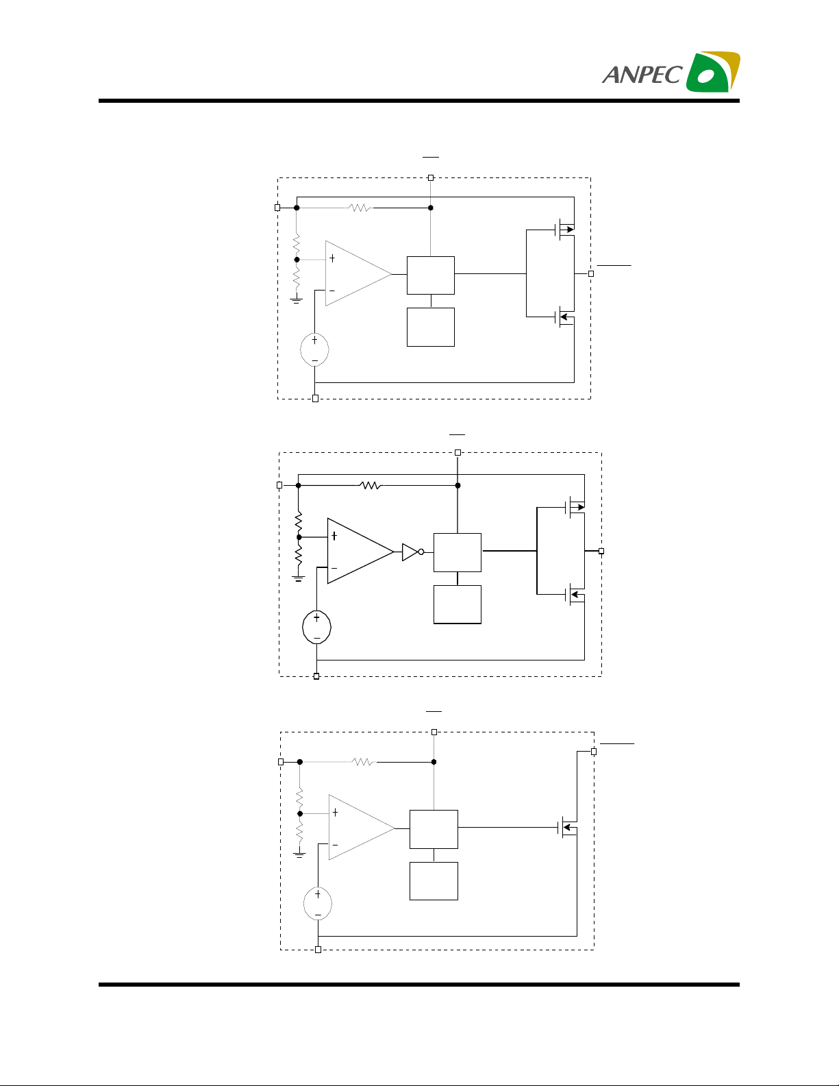
Block Diagram
c c
V
MR
Reset
Generator
+ Timer
Oscillator
REF
V
RESET
GND
APR3101
MR
c c
V
Reset
GND
Generator
+ Timer
Oscillator
V
REF
APR3102
RESET
MR
c c
V
RESET
Copyright ANPEC Electronics Corp.
Rev. A.3 - Feb., 2004
GND
Reset
Generator
+ Timer
Oscillator
V
REF
APR3103
www.anpec.com.tw3
Page 4
APR3101/2/3
Part Number Description
Part Number Part Description
APR3101 Reset Output Push Pull Active Low with Delay
APR3102 Reset Output Push Pull Active High with Delay
APR3103 Reset Output Open Drain Active Low with Delay
Electrical Characteristics
VIN = 5V, TA = -40 to 85°C unless otherwise noted. Typical values are at TA=25°C, VCC = 5V for 4.38V
versions, VCC = 3.3V for 3.08/2.93V versions, VCC = 3.0V for 2.63V. versions and VCC = 2.5V for 2.32V
versions, VCC = 2.0V for 1.75V versions , VCC = 1.8V for 1.5V versions.
Symbol Parameter Test Conditions
VCC
V
T
VOH
T
T
V
V
RMR
Supply Voltage
ICC
Supply Current V
T
VTH
Reset Threshold
Hysteresis Range 20 mV
HYST
Reset Timeout Period
RTP
VOL
Reset Output Low I
Reset Output High I
TD
V
to Reset Delay VCC=VTH to (VTH-100mV) 25
CC
ILE
Reset Output Leakage 0.5
MR Minimum Pulse Width 10
MPW
MR to Reset Delay 0.5
MRD
MR Input Low Threshold 0.4* V
MIL
MR Input High Threshold 0.5* V
MIH
MR Pull-Up resistance
=1.5V~6V 1.5 4
CC
=-40 to 85°C 3 5
A
T A=25°C ±1.5%
T
=-40 to 85°C ±2%
A
150 250 350
=1.2mA 0.5 V
SINK
=0.6mA 0.8*VCC
SOURCE
APR3101/2/3
Min. Typ. Max.
1.2 6
V
CC
CC
30 47 70
Unit
V
µ
A
ms
µ
S
µ
A
µ
S
µ
S
KΩ
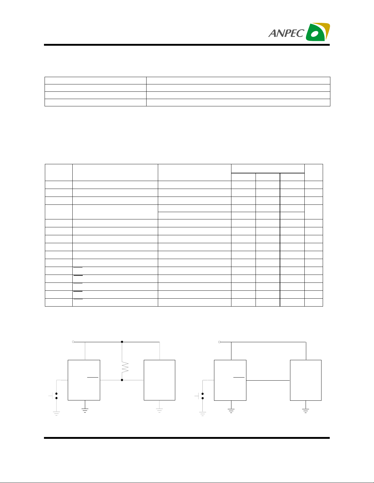
Application Circuit
CC
V
CC
V
APR3103 RESET
GND
Copyright ANPEC Electronics Corp.
Rev. A.3 - Feb., 2004
100k
RESET
INPUT
V
µ
GND
CC
V
CC
P
APR3101
APR3102
CC
V
GND
RESET
(RESET)
CC
V
RESET
P
µ
INPUT
GND
www.anpec.com.tw4
Page 5
APR3101/2/3
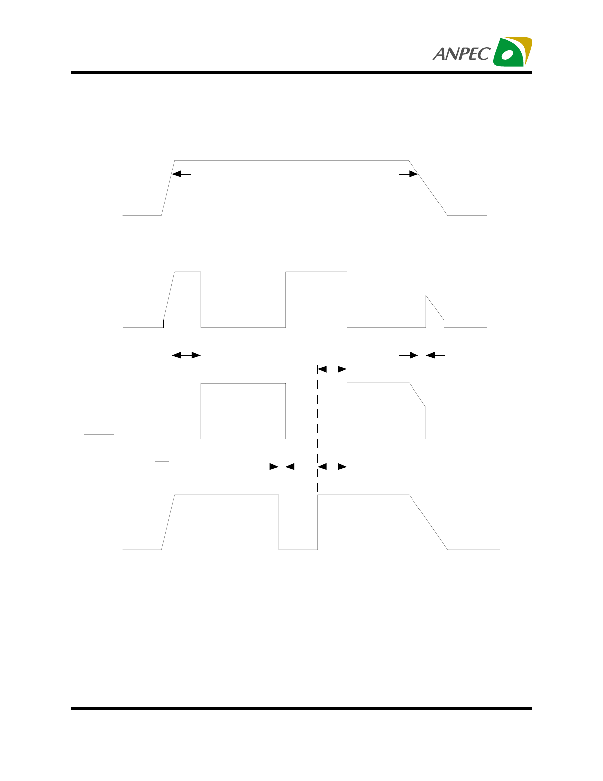
Timing Chart
Vcc
(APR3102)
RESE T
Reset Threshold Reset Threshold
(APR3101/ 3)
RESE T
MR
Reset Timeout P eriod 250ms
MR to Reset Delay 0.5us
Vc c t o Res et Delay 25us
Reset Timeout P eriod 250ms
Copyright ANPEC Electronics Corp.
Rev. A.3 - Feb., 2004
www.anpec.com.tw5
Page 6

APR3101/2/3
Typical Characteristics
Supply Current vs. Supply Voltage
2
Maximum Transient Duration vs.
Reset Threshold Overdrive VTH - VCC
120
1.6
1.2
0.8
0.4
Supply Current (uA)
0
0123456
Supply Voltage (V)
Output Source Current vs. Reset High Output Voltage
70
Vcc=5 V
60
50
Vcc=4 V
40
30
Vcc=3 V
20
10
Output Source Current (mA)
0
0123456
Reset High Output Voltage (V)
100
80
60
40
20
never generate a reset signal
Maximum Transient Duration (us)
0
10 100 1000
generate a reset signal
Reset Threshold Overdrive VTH - VCC (mV)
Output Sink Current vs. Reset Low Output Voltage
50
45
40
35
30
25
20
15
10
5
Output Sink Current (mA)
0
0123456
Vcc=1.5
Vcc=2.9V
Vcc=2.5V
Vcc=2V
Reset Low Output Voltage (V)
Copyright ANPEC Electronics Corp.
Rev. A.3 - Feb., 2004
www.anpec.com.tw6
Page 7

APR3101/2/3
Typical Characteristics
Normalized Reset Threshold vs. T emperature
1.008
1.006
1.004
1.002
1
0.998
0.996
Normalized Reset Threshold (%)
0.994
-40 -20 0 20 40 60 80 100 120
Temperature (°C)
600
Reset Propagation Delay vs. T emperature
60
50
40
VOD=100mV
30
20
10
Reset Propagation Delay (us)
0
-40 -20 0 20 40 60 80 100 120
Temperature (°C)
Supply Current vs. T emperature Reset Timeout Period vs. Temperature
3.5
500
400
300
200
100
Reset Timeout Period (ms)
0
-40-200 20406080100120
T emperature (°C)
Copyright ANPEC Electronics Corp.
Rev. A.3 - Feb., 2004
3
2.5
2
1.5
1
Supply Current (uA)
0.5
0
-40-200 20406080100120
Vcc=5V
Vcc=3V
T emperature (°C)
www.anpec.com.tw7
Page 8

APR3101/2/3
Typical Characteristics
Power Up
Vcc(2V/div)
RESET(2V/div)
MR(2V/div)
Vcc(2V/div)
RESET(2V/div)
MR(2V/div)
Power Down
Time (50ms/div) Time (500ms/div)
MR to Reset Delay
Vcc to RESET Delay
Time (0.2us/div)
Copyright ANPEC Electronics Corp.
Rev. A.3 - Feb., 2004
Vcc(2V/div)
RESET(2V/div)
MR(2V/div)
Vcc(0.5V/div)
Vcc=VTH to (VTH-100mV)
RESET(2V/div)
Time (10us/div)
www.anpec.com.tw8
Page 9

APR3101/2/3
Typical Characteristics
Manual Reset
Vcc(2V/div)
RESET(2V/div)
MR(2V/div)
Time (100ms/div)
Copyright ANPEC Electronics Corp.
Rev. A.3 - Feb., 2004
www.anpec.com.tw9
Page 10

APR3101/2/3
Application Information
VCC Transient Rejection
The APR3101/2/3 have the function to reject the transient glitches from the power line. The Maximum Transient Duration vs. Reset Threshold Overdrive shows
at Typical Characteristics. The transient voltage with
the duration under the curve will not generate a reset
signal, e.g. a transient of 100mV below the reset
threshold voltage have the duration more than 35us, it
will generate a reset signal. Connect a 0.1uF bypass
capacitor to the VCC pin can improve the transient
immunity.
Manual Reset Input
Force the MR low asserts the reset signal, asserted
reset continues as long as MR is low and after the
MR goes high the reset signal is maintained for a fixed
timeout period. The MR is internally connected a 47kΩ
resistor to VCC, so it can be floating if MR is not used.
The MR input also has a debounce time 500ns to avoid
the glitches. It allows use of a mechanical switch or a
TTL, and CMOS logic signal.
the IC is shutdown, and the output becomes a floating
state. If it is a trouble, a resistor should be connected
from reset output to ground to keep the reset output
low (see Figure 1). For The APR3102, a pull-up resistor to VCC is required to keep the valid reset output for
VCC below 1.2V.
¡@¡@
¡@
¡@¡@
V
CC
V
CC
RESET
GND
100K
Figure 1. Ensuring RESET Valid to VCC = 0 V
+3.3V +5.0V
Reset Output
The APR3101/2/3 have 3 output stage versions:
APR3101 is an active low push-pull output,when the
VCC drops below the reset threshold or MR goes low,
the RESET output generates a low signal. APR3102
is an active high push-pull output, when the VCC drops
below the reset threshold or MR goes low; the RESET output generates a high signal (see Timing Chart).
APR3103 is an active low open drain output, the RESET output must be connected a pull-up resistor to a
supply voltage that is lower than 6V, it suits to use in
multiple voltage systems (see Figure 2). The APR3101
RESET output is valid until the VCC=1.2V, below 1.2V
Copyright ANPEC Electronics Corp.
Rev. A.3 - Feb., 2004
APR3103
MR
V
RESET
GND
CC
100k
VCC
RESET
INP U T5VSystem
GND
Figure 2. APR3103 Open Drain Output with Multiple
Supplies
www.anpec.com.tw10
Page 11

APR3101/2/3
Packaging Information
SOT-23-5
e1
45
12
3
E1 E
e
D
Dim
Min. Max. Min. Max.
A 0.95 1.45
A1 0.05 0.15
A2 0.90 1.30
b 0.30 0.50
D 2.8 3.00
E 2.6 3.00
E1 1.5 1.70
e 0.95BSC
e1 1.90BSC
L 0.35 0.55
b
A2
A
A1 L 2
L
L 1
a
Millimeters Inches
0.037 0.057
0.002 0.006
0.035 0.051
0.011 0.019
0.110 0.118
0.102 0.118
0.059 0.067
0.037BSC
0.074BSC
0.014 0.022
L1 0.20 BSC 0.008 BSC
L2 0.5 0.7
0.020 0.028
N 5 5
α
0
°
10° 0
°
10°
Copyright ANPEC Electronics Corp.
Rev. A.3 - Feb., 2004
www.anpec.com.tw11
Page 12

APR3101/2/3
Physical Specifications
Ter minal Material Solder-Plated Copper (Solde r Ma terial : 90/10 or 63/3 7 SnP b) , 100 %Sn
Lead Solderability Meets EIA Spe c ification RSI86-91, ANSI/J-ST D-002 Category 3.
Reflow Condition (IR/Convection or VPR Reflow)
T
P
Ramp-up
T
L
Tsmax
Tsmin
Temp erature
ts
Preheat
25
°
t 25 C to Pe a k
Classificatin Reflow Profiles
tp
Ramp-down
Time
Critical Zone
to T
T
L
P
t
L
Profile Feature Sn-Pb Eutectic Assembly Pb-Free Assembly
Large Body Small Body Large Body Small Body
Average ramp-up rate
(T
to TP)
L
Preheat
- Temperature Min (Tsmin)
- Temperature Mix (Tsmax)
- Time (min to max)(ts)
Tsmax to TL
- Temperature(T
- Time (t
)
L
)
L
Peak Temperature(Tp)
Time within 5°C of actual Peak
Temperature(tp)
225 +0/-5°C 240 +0/-5°C 245 +0/-5°C 250 +0/-5°C
3°C/second max. 3°C/second max.
100°C
150°C
60-120 seconds
150°C
200°C
60-180 seconds
3°C/second max
183°C
60-150 seconds
217°C
60-150 seconds
Ramp-down Rate 10-30 seconds 10-30 seconds 10-30 seconds 20-40 seconds
Time 25°C to Peak Temperature 6°C/second max. 6°C/second max.
6 minutes max. 8 minutes max.
Note: All temperatures refer to topside of the package. Measured on the body surface.
Copyright ANPEC Electronics Corp.
Rev. A.3 - Feb., 2004
www.anpec.com.tw12
Page 13

APR3101/2/3
Relia b ility te st progra m
SOLDERA BILITY MIL-STD-883D-2003
HO LT MIL-STD-883D-1005.7
PCT JESD-22-B, A102
TST MIL-STD-883D -1011.9
245°C , 5 SEC
1000 Hrs Bias @ 125 °C
168 Hrs, 100 % RH , 121°C
-65°C ~ 150°C, 200 Cycles
ESD M IL-STD-883D-3015.7 VHBM > 2KV, VMM > 200V
La tc h -Up JES D 78 10 ms , Itr > 100mA
Carrier Tape
t
Test item Method D escriptio n
E
F
W
Po
P
P1
Ao
D
Bo
Ko
D1
A
Application
A B C J T1 T2 W P E
178±172 ± 1.0 13.0 + 0.2 2.5 ± 0.15 8.4 ± 2 1.5± 0.3
SOT-23-5
F D D1 Po P1 Ao Bo Ko t
3.5 ± 0.05 1.5 +0.1 1.5 +0.1 4.0 ± 0.1 2.0 ± 0.1 3.15 ± 0.1 3.2± 0.1 1.4± 0.1 0.2±0.03
Copyright ANPEC Electronics Corp.
Rev. A.3 - Feb., 2004
T2
J
C
B
T1
8.0+ 0.3
- 0.3
4 ± 0.1 1.75± 0.1
(mm)
www.anpec.com.tw13
Page 14

APR3101/2/3
Cover Tape Dimensions
Application Carrier Width Cover Tape Width Devices Per Reel
SOT- 23
Customer Service
Anpec Electronics Corp.
Head Office :
5F, No. 2 Li-Hsin Road, SBIP,
Hsin-Chu, T aiwan, R.O.C.
T el : 886-3-5642000
Fax : 886-3-5642050
Taipei Branch :
7F, No. 137, Lane 235, Pac Chiao Rd.,
Hsin Tien City, Taipei Hsien, Taiwan, R. O. C.
T el : 886-2-89191368
Fax : 886-2-89191369
8 5.3 3000
Copyright ANPEC Electronics Corp.
Rev. A.3 - Feb., 2004
www.anpec.com.tw14
 Loading...