

Page 1
APM3054N
N-Channel Enhancement Mode MOSFET
Features
• 30V/15A, R
R
••
•
Super High Dense Cell Design
••
••
• High Power and Current Handling Capability
••
••
• TO-252 and SOT-223 Package
••
=48mΩ(typ.) @ VGS=10V
DS(ON)
=75mΩ(typ.) @ VGS=4.5V
DS(ON)
Pin Description
G DS
Top View of TO-252
Applications
123
• Switching Regulators
• Switching Converters
GDS
Top View of SOT-89
Ordering and Marking Information
APM 3054N
Handling Code
Temp. R ange
Package Code
Package Code
D : S O T -89 U : TO-2 52 V : S O T -22 3
Operating Junction Temp. Range
C : -55 to 125 C
Handling Code
TR : Tape & Reel
123
°
123
SDG
Top View of SOT-223
APM 3054N U :
APM3054N D/V :
APM 3054N
XXXXX
APM 3054N
XXXXX
Absolute Maximum Ratings (T
Symbol
V
DSS
V
GSS
I
D
I
DM
I
S
ANPEC reserves the right to make changes to improve reliability or manufacturability without notice, and advise
customers to obtain the latest version of relevant information to verify before placing orders.
Copyright ANPEC Electronics Corp.
Rev. A.2 - Aug., 2002
Drain-Sour ce Voltage 30
Gate-Source Voltage ±20
Maximum Drain Current – Continuous 15
Maximum Drain Current – Pulsed 30
Diode Con t in uous Forwar d Current 8 A
Parameter Rating Unit
XXXXX
XXXXX - Date Code
= 25°C unless otherwise noted)
A
- Da te C o d e
V
A
www.anpec.com.tw1
Page 2
APM3054N
Absolute Maximum Ratings (Cont.) (T
Symbol
I
SM
Diode Maximum Pulse Current 32 A
Parameter Rating Unit
= 25°C unless otherwise noted)
A
TA=25°C
P
D
T
J
T
STG
Electrical Characteristics (T
Maxim um Power Dissipation
=100°C
T
A
Maximum Junction Temperature
Storage Tem perature Range -55 to 150 °C
= 25°C unless otherwise noted)
A
Symbol Paramet er Test Condition
Static
BV
I
V
DSS
GS(th)
Drain-Source Breakdown
DSS
Voltage
Zero Gate Voltage Drain
Current
Gate Threshold Voltage
V
=0V, IDS=250µA
GS
V
=24V, VGS=0V 1
DS
V
DS=VGS
, IDS=250µA
TO-252 62.5
SOT-223 3
TO-252 25
SOT-223 1.2
150 °C
APM3054N
Min. Typ. Max.
30 V
13V
W
W
Unit
µ
A
I
GSS
R
DS(ON)
V
SD
Dynamic
Q
g
Q
gs
Q
gd
t
d(ON)
t
r
t
d(OFF)
t
f
C
iss
C
oss
C
rss
Gate Leakage Current
Drain-Source On-state
Resistance
=±20V, VDS=0V
V
GS
±
100
VGS=10V, IDS=12A 48 54
=4.5V, IDS=6A 75 90
V
GS
nA
m
Diode For w ar d Voltage ISD=8A, VGS=0V 0.6 1.3 V
Total Ga te Charge 9
=15V, VGS=5V,
V
Gate-Source Charge 5.4
Gate-Drain Charge
I
DS
DS
=10A
nC
2.4
Turn-on Delay Time 11
Turn-on Rise Time 17
Turn-off Delay Time 37
Turn-off Fall Time
Input Capacitance 400
Output Ca pacitance 75
Reverse Transfer
V
=15V,ID=2A,
DD
V
=10V, RG=6
GS
V
=0V
GS
V
=25V
DS
Ω
Frequency=1.0MHz
ns
20
pF
45
Ω
Copyright ANPEC Electronics Corp.
Rev. A.2 - Aug., 2002
www.anpec.com.tw2
Page 3
APM3054N
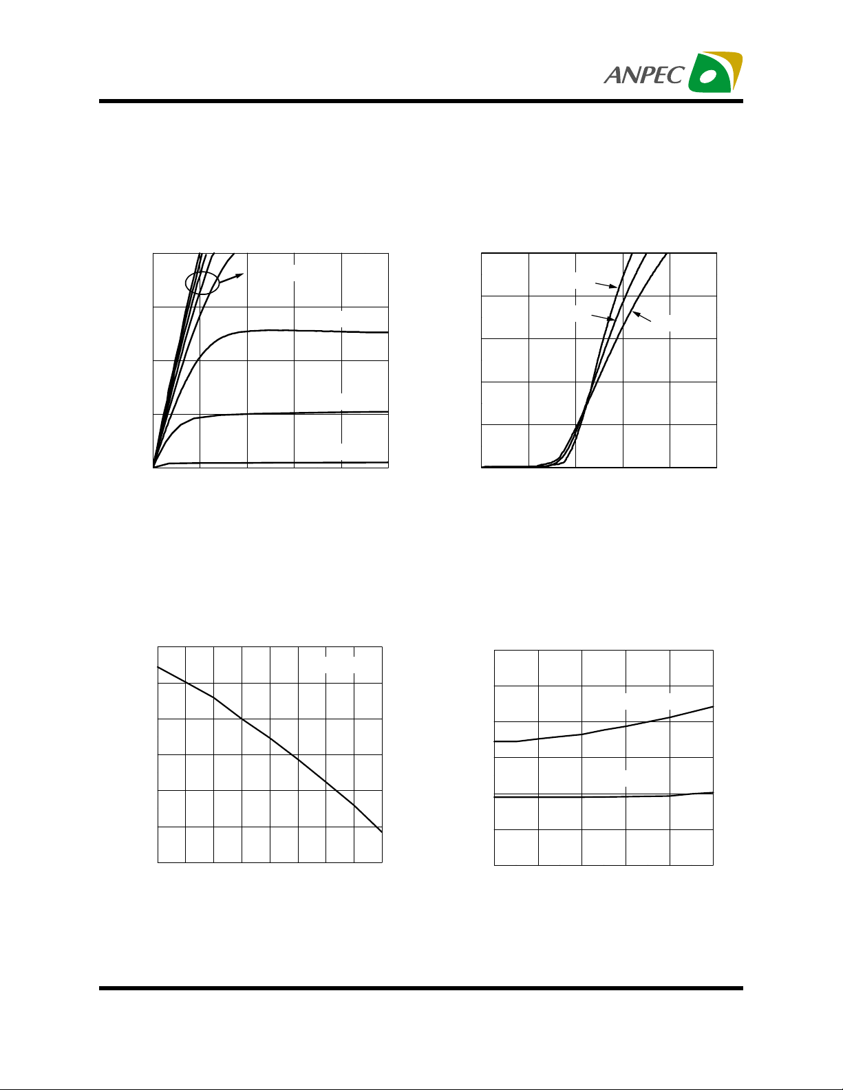
Typical Characteristics
Output Characteristics
20
15
10
5
ID-Drain Current (A)
0
012345
VGS=6,7,8,9,10V
VGS=5V
VGS=4V
VGS=3V
VDS - Drain-to-Source V oltage (V)
Threshold Voltage vs. Temperature
1.2
1.1
1.0
IDS=250uA
Transfer Characteristics
25
TJ=-55°C
20
TJ=25°C
15
10
TJ=125°C
ID-Drain Current (A)
5
0
0246810
VGS - Gate-to-Source V oltage (V)
On-Resistance vs. Drain Current
0.12
0.10
0.08
VGS=4.5V
0.9
(Normalzed)
0.8
0.7
VGS(th)-Threshold Voltage (V)
0.6
-50 -25 0 25 50 75 100 125 150
Tj - Junction T emperature (°C)
Copyright ANPEC Electronics Corp.
Rev. A.2 - Aug., 2002
0.06
VGS=10V
0.04
RDS(on)-On-Resistance (Ω)
0.02
0.00
0246810
ID - Drain Current (A)
www.anpec.com.tw3
Page 4
APM3054N
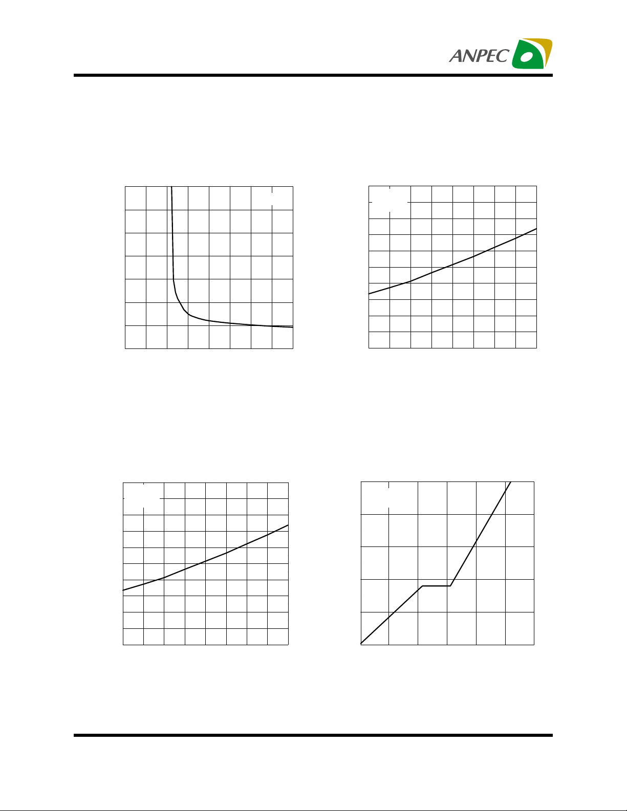
Typical Characteristics
On-Resistance vs. Gate-to-Source Voltage
0.35
0.30
0.25
0.20
ID=6A
0.15
0.10
RDS(on)-On-Resistance (Ω)
0.05
0.00
2345678910
VGS - Gate-to-Source V oltage (V)
On-Resistance vs. Junction T emperature
0.10
VGS=10V
IDS=12A
0.09
0.08
0.07
0.06
0.05
0.04
0.03
0.02
RDS(on)-On-Resistance (Ω)
0.01
0.00
-50 -25 0 25 50 75 100 125 150
TJ - Junction Temperature (°C)
On-Resistance vs. Junction T emperature
0.10
VGS=10V
0.09
ID=12A
0.08
0.07
0.06
0.05
0.04
(Normalized)
0.03
0.02
RDS(on)-On-Resistance (Ω)
0.01
0.00
-50 -25 0 25 50 75 100 125 150
TJ - Junction Temperature (°C)
Gate Charge
10
VDS=15V
IDS=10A
8
6
4
2
VGS-Gate-Source Voltage (V)
0
2.5 5.0 7.5 1 0.0 12.5 15.0
QG - Gate Charge (nC)
Copyright ANPEC Electronics Corp.
Rev. A.2 - Aug., 2002
www.anpec.com.tw4
Page 5

APM3054N
Typical Characteristics
Capacitance
750
625
500
Ciss
375
250
Capacitance (pF)
125
0
0 5 10 15 20 25 30
VDS - Drain-to-Source Voltage (V)
Single Pulse Power
250
Coss
Crss
TO-252
Source-Drain Diode Forward Voltage
30
10
IS-Source Current (A)
TJ=150°C
1
0.0 0.2 0.4 0.6 0.8 1.0 1.2 1.4 1.6 1.8 2.0
TJ=25°C
VSD -Source-to-Drain V oltage (V)
Single Pulse Power
140
SOT-223
200
150
100
Power (W)
50
0
1E-3 0.01 0.1 1 10 100 1000
Time (sec)
Copyright ANPEC Electronics Corp.
Rev. A.2 - Aug., 2002
120
100
80
60
Power (W)
40
20
0
0.01 0.1 1 10 100 1000
Time (sec)
www.anpec.com.tw5
Page 6

APM3054N
Typical Characteristics
Normalized Thermal Transient Impedence, Junction to Ambient
1
Duty Cycle=0.5
D=0.2
D=0.1
D=0.05
0.1
D=0.02
D=0.01
Thermal Impedance
SINGLE PULSE
Normalized Effective Transient
0.01
1E-4 1E-3 0.01 0.1 1 10 100 1000
Square Wave Pulse Duration (sec)
Normalized Thermal Transient Impedence, Junction to Ambient
1.Duty Cycle, D=t1/t2
2.Per Unit Base=RthJA=50°C/W
3.TJM-TA=PDMZthJA
TO-252
SOT-223
1
Duty Cycle = 0.5
D= 0.2
0.1
D= 0.1
D= 0.05
D= 0.02
0.01
D= 0.01
Thermal Impedance
SINGLE PULSE
Normalized Effective Transient
1E-3
1E-4 1E-3 0.01 0.1 1 10 100 1000
Copyright ANPEC Electronics Corp.
Rev. A.2 - Aug., 2002
Square Wave Pulse Duration (sec)
1.Duty Cycle, D=t1/t2
2.Per Unit Base=RthJA=42°C/W
3.TJM-TA=PDMZthJA
www.anpec.com.tw6
Page 7

APM3054N
Package Information
SOT-89 (Reference EIAJ ED-7500A Reg stration SC-62)
D
D1
H
L
123
a
E
C
Dim
B1
B
e
e1
A
a
Millimeters Inches
Min. Max. Min. Max.
A 1.40 1.60 0.055 0.063
B 0.40 0.56 0.016 0.022
B1 0.35 0.48 0.014 0.019
C 0.35 0.44 0.014 0.017
D 4.40 4.60 0.173 0.181
D1 1.35 1.83 0 .053 0.072
e 1.50 BSC 0.059 BSC
e1 3.00 B SC 0.118 BSC
E 2.29 2.60 0.090 0.102
H 3.75 4.25 0.148 0.167
L 0 .80 1.20 0.031 0.047
α
10
°
10
°
Copyright ANPEC Electronics Corp.
Rev. A.2 - Aug., 2002
www.anpec.com.tw7
Page 8

APM3054N
Package Information
TO-252( Reference JEDEC Registration TO-252)
E
b2
A
C1
L2
D
H
L1
L
b
e1
C
A1
Dim
A 2.18 2.39 0.086 0.094
A1 0.89 1.27 0.035 0.050
b 0.508 0.89 0.020 0.035
b2 5.207 5.4 61 0.205 0.215
C 0.46 0.58 0.018 0.023
C1 0.46 0.58 0.018 0.023
D 5.334 6.22 0.210 0.2 45
E 6.35 6.73 0.250 0.265
e1 3.96 5.18 0.156 0.204
H 9.398 10.41 0.370 0.410
L 0.51 0.020
L1 0.64 1.02 0.025 0.040
L2 0.89 2.032 0. 035 0. 080
Copyright ANPEC Electronics Corp.
Rev. A.2 - Aug., 2002
Min. Max. Min . Max .
Millimeters Inches
www.anpec.com.tw8
Page 9

APM3054N
Package Information
SOT-223( Reference JEDEC Registration SOT-223)
D
B1
H E
K
e
e1
B
A
A1
b
a
c
L
Millimeters InchesDim
Min. Max. Min. Max.
A 1.50 1.80 0.06 0.07
A1 0.02 0.08
B 0.60 0.80 0.02 0.03
B1 2.90 3.10 0.11 0.12
c 0.28 0.32 0.01 0.01
D 6.30 6.70 0.25 0.26
E 3.30 3.70 0.13 0.15
e 2.3 BSC 0.09 BSC
e1 4.6 BSC 0.18 BSC
H 6.70 7.30 0.26 0.29
L 0.91 1.10 0.04 0.04
K 1.50 2.00 0.06 0.08
α
β
Copyright ANPEC Electronics Corp.
Rev. A.2 - Aug., 2002
0
°
13
°
10
°
0
°
13
10
°
°
www.anpec.com.tw9
Page 10

APM3054N
Physical Specifications
Terminal Material Solder-Plated Copper (Solder Material : 90/10 or 63/37 SnPb)
Lead Solderability Meets EIA Specification RSI86-91, ANSI/J-STD-002 Category 3.
Reflow Condition (IR/Convection or VPR Reflow)
Reference JEDEC Standard J-STD-020A APRIL 1999
Peak temperature
temperature
Pre-heat temperature
°
183 C
Time
Classification Reflow Profiles
Convection or IR/
Convection
Average ramp-up rate(183°C to Peak) 3°C/second max. 10 °C /second max .
Preheat temperature 125 ± 25°C)
Temperature maintained above 183°C
Time within 5°C of actual peak temperature
Peak temperature range
Ramp-down rate
Time 25°C to peak temperature
120 seconds max
60 – 150 seconds
10 –20 seconds 60 seconds
220 +5/-0°C or 235 +5/-0°C 215-219°C or 235 +5/-0°C
6 °C /second max . 10 °C /second max .
6 minutes max.
VPR
Package Reflow Conditions
pkg. thickness
and all bgas
Convection 220 +5/-0 °C Convection 235 +5/- 0 °C
VPR 215-219 °C VPR 235 +5/-0 °C
IR/Convection 220 +5/-0 °C IR/Convection 235 +5/-0 °C
Copyright ANPEC Electronics Corp.
Rev. A.2 - Aug., 2002
2.5mm
≥≥≥≥
pkg. thickness < 2.5mm and
pkg. volume
350 mm³
≥≥≥≥
pkg. thickness < 2.5mm and pkg.
volume < 350mm³
www.anpec.com.tw10
Page 11

APM3054N
R e lia bility t e s t p r o g ra m
SOLDERA BILITY MIL-STD-883D-2003
HO LT MIL-STD-883D-1005.7
PCT JESD-22-B, A102
TST MIL-STD-883D-1011.9
245°C , 5 SEC
1000 Hrs Bias @ 125 °C
168 Hrs, 100 % RH , 121°C
-65°C ~ 150°C, 200 Cycles
ESD MIL-STD-883D-3015.7 VHBM > 2KV, VMM > 200V
La tc h -Up JES D 78 10 ms , Itr > 100mA
Test item Method Descrip tion
Carrier Tape
W
E
F
Po
P
P1
Ao
D
Bo
D1
t
Ko
T2
J
C
A
B
T1
Copyright ANPEC Electronics Corp.
Rev. A.2 - Aug., 2002
www.anpec.com.tw11
Page 12

APM3054N
Application
SOT-89
Application
TO-252
Application
SOT-223
A B C J T1 T2 W P E
178 ±170 ± 213.5 ± 0.15 3 ± 0.15 14 ± 2 1.3 ± 0.3
F D D1 Po P1 Ao Bo Ko t
5.5 ± 0.05 1.5± 0.1 1.5± 0.1 4.0 ± 0.1 2.0 ± 0.1 4.8 ± 0.1 4.5± 0.1 1.80± 0.1 0.3±0.013
A B C J T1 T2 W P E
330 ±3100 ± 213 ± 0. 5 2 ± 0.5
F D D1 Po P1 Ao Bo Ko t
7.5 ± 0.1 1.5 +0.1 1.5± 0.25 4.0 ± 0.1 2.0 ± 0.1 6.8 ± 0.1 10.4± 0.1 2.5± 0.1 0.3±0.05
A B C J T1 T2 W P E
12.75
330±162±1.5
F D D1 Po P1 Ao Bo Ko t
5.5 ± 0.05 1.5+ 0.1 1.5+ 0.1 4.0 ± 0.1 2.0 ± 0.05 6.9 ± 0.1 7.5± 0.1 2.1± 0.1 0.3±0.05
0.15
±
Cover Tape Dimensions
Application Carrier Width Cover Tape Width Devices Per Reel
SOT- 89
SOT- 223
TO- 252
12 9.3 1000
12 9.3 2500
16 13.3 2500
12 + 0.3
12 - 0.1
16.4 + 0.3
-0.2
2 ± 0.6 12.4 +0.2 2± 0.2 12 ± 0.3 8 ± 0.1 1.75± 0.1
2.5± 0.5
16+ 0.3
- 0.1
8 ± 0.1 1.75± 0.1
8 ± 0.1 1.75± 0.1
Customer Service
Anpec Electronics Corp.
Head Office :
5F, No. 2 Li-Hsin Road, SBIP,
Hsin-Chu, T aiwan, R.O.C.
T el : 886-3-5642000
Fax : 886-3-5642050
Taipei Branch :
7F, No. 137, Lane 235, Pac Chiao Rd.,
Hsin Tien City, T aipei Hsien, Taiwan, R. O. C.
T el : 886-2-89191368
Fax : 886-2-89191369
Copyright ANPEC Electronics Corp.
Rev. A.2 - Aug., 2002
www.anpec.com.tw12
 Loading...