

Page 1
N-Channel Enhancement Mode MOSFET
Copyright ANPEC Electronics Corp.
Rev. A.3 - Jan., 2003
APM3005N
www.anpec.com.tw1
ANPEC reserves the right to make changes to improve reliability or manufacturability without notice, and advise
customers to obtain the latest version of relevant information to verify before placing orders.
APM 3005N
Handling Code
Temp. Range
Package Code
Package Code
F : T O -2 2 0 U : T O-25 2 G : T O -2 6 3
Operating Junction Temp. Range
C : -5 5 to 1 2 5 C
Handling Code
T U : Tu b e
TR : Tape & Reel
°°°°
APM 3005N :
APM3005N
XXXXX
- Da te C o d e
XXXXX
Pin Description
Ordering and Marking Information
Features
Applications
Absolute Maximum Ratings
(TA = 25°C unless otherwise noted)
• 30V / 80A , R
DS(ON)
= 4mΩ(typ.) @ VGS= 10V
R
DS(ON)
= 7mΩ(typ.) @ VGS= 4.5V
• Super High Dense Advanced Cell Design for
Extremely Low R
DS(ON)
• Reliable and Rugged
• TO-220, TO-252 and TO-263 Packages
• Power Management in Desktop Computer or
DC/DC Converters.
T op View of T O-220, TO-252 and T O-263
Symbol
Parameter Rating Unit
V
DSS
Drain-Source Voltage 30
V
GSS
Gate-Source Voltage ±20
V
I
D
*
Maximum Drain Current – Continuous 80
I
DM
Maximum Drain Current – Pulsed 160
A
G
DS
123
G
S
D
N-Channel MOSFET
Page 2
Copyright ANPEC Electronics Corp.
Rev. A.3 - Jan., 2003
APM3005N
www.anpec.com.tw2
APM3005N
Symbol Parameter Test Condition
Min. T
y
p. Max.
Unit
Static
BV
DSS
Drain-Source Breakdown
Voltage
V
GS
=0V , IDS=250µA
30 V
I
DSS
Zero Gate Voltage Drain
Current
V
DS
=24V , VGS=0V 1 µA
V
GS(th)
Gate Threshold Voltage
V
DS=VGS
, IDS=250µA
11.52
V
I
GSS
Gate Leakage Current
V
GS
=±20V , VDS=0V
±
100
nA
VGS=10V , IDS=80A
45.4
R
DS(ON)
a
Drain-Source On-state
Resistance
V
GS
=4.5V , IDS=70A
78
m
Ω
V
SD
a
Diode Forward Voltage ISD=30A , VGS=0V
0.85 1.3
V
Dynamic
b
Q
g
Total Gate Charge
28 32
Q
gs
Gate-Source Charge
12.8
Q
gd
Gate-Drain Charge
VDS=15V , IDS= 80A
V
GS
=5V ,
21.2
nC
t
d(ON)
Turn-on Delay Time
13 20
T
r
Turn-on Rise Time
915
t
d(OFF)
Turn-off Delay Time
43 66
T
f
Turn-of f Fall Time
V
DD
=15V , IDS=1A ,
V
GEN
=10V , RG=0.2
Ω
14 28
ns
C
iss
Input Capacitance
4700
C
oss
Output Capacitance
930
C
rss
Reverse Transfer Capacitance
VGS=0V
V
DS
=15V
Frequency=1.0MHz
280
pF
Symbol Parameter Rating Unit
TO-252 50
TA=25°C
TO-263 62.5
W
TO-252 20
P
D
Maximum Power Dissipation
T
A
=100°C
TO-263 25
W
TJ,T
STG
Maximum O p era t ing and Storage Junction Temperature -55 to 150
°
C
TO-252 50
R
θ
JA
Thermal Resistance – Junction to Ambient
TO-263 60
°
C/W
TO-252 2.5
R
θ
JC
Thermal Resistance – Junction to Case
TO-263 2
°
C/W
* Surface Mounted on FR4 B oard, t ≤ 10 sec.
Notes
a
: Pulse test ; pulse width ≤300µs, duty cycle ≤ 2%
b
: Guaranteed by design, not subject to production testing
Electrical Characteristics (T
A
= 25°C unless otherwise noted)
Absolute Maximum Ratings (Cont.) (T
A
= 25°C unless otherwise noted)
Page 3
Copyright ANPEC Electronics Corp.
Rev. A.3 - Jan., 2003
APM3005N
www.anpec.com.tw3
0 20 40 60 80 100 120
0.000
0.002
0.004
0.006
0.008
0.010
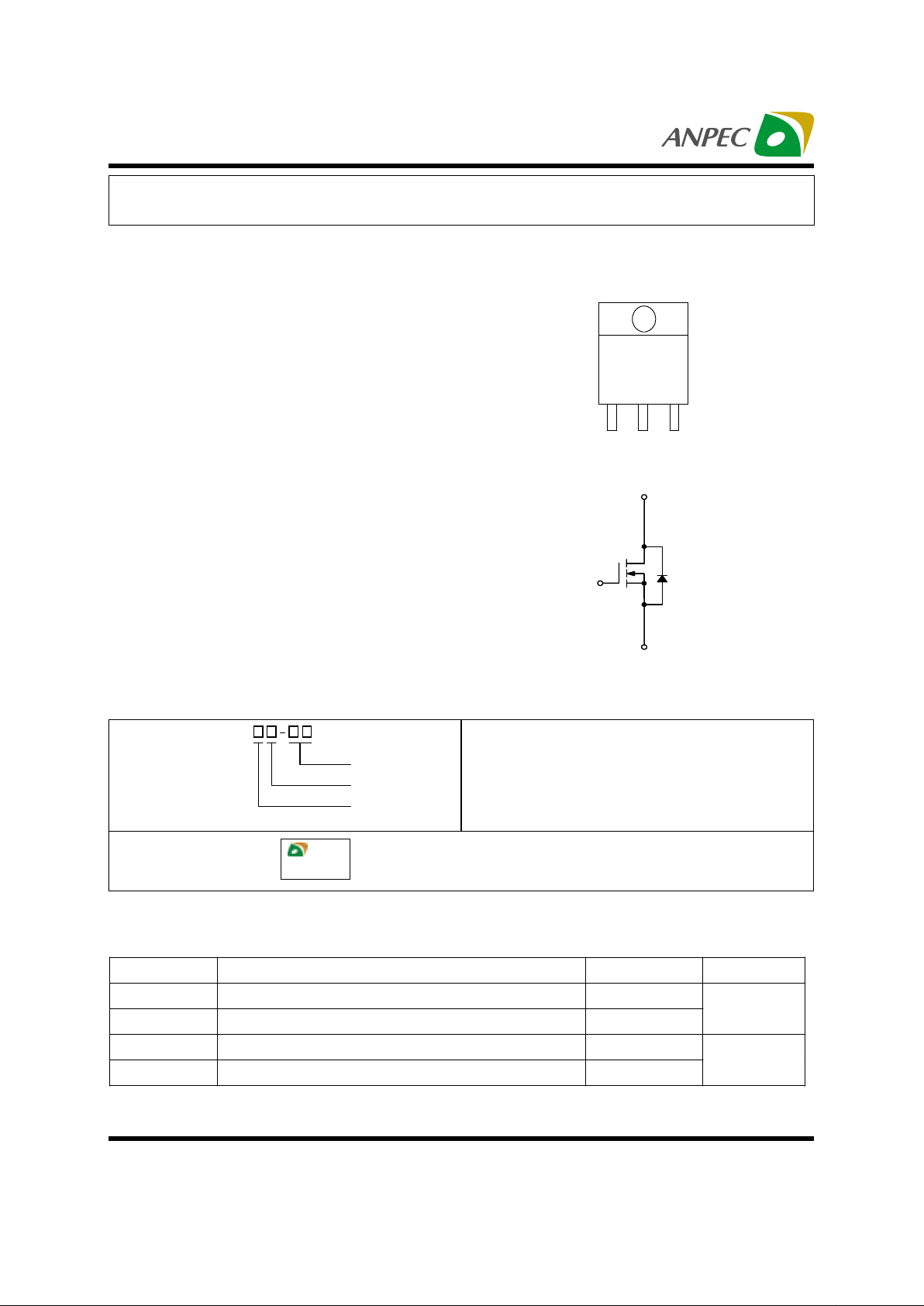
Typical Characteristics
012345
0
20
40
60
80
Output Characteristics
V
DS
-Drain-to-Source Voltage (V)
I
DS
-Drain Current (A)
VGS=4,5,6,7,8,9,10V
VGS=3V
VGS=3.5V
0123456
0
20
40
60
80
100
VGS-Gate-to-Source Voltage (V)
Transfer Characteristics
I
DS
-Drain Current (A)
TJ=125°C
TJ=25°C
TJ=-55°C
On-Resistance vs. Drain Current
IDS-Drain Current (A)
R
DS(ON)
-On-Resistance (Ω)
VGS=10V
VGS=4.5V
-50 -25 0 25 50 75 100 125 150
0.2
0.4
0.6
0.8
1.0
1.2
1.4
Threshold Voltage vs. Junction Temperature
Tj-Junction T emperature (°C)
V
GS(th)
-Threshold Voltage (V)
(Normalized)
IDS=250µA
Page 4
Copyright ANPEC Electronics Corp.
Rev. A.3 - Jan., 2003
APM3005N
www.anpec.com.tw4
0 102030405060708090
0
2
4
6
8
10
-50 -25 0 25 50 75 100 125 150
0.4
0.6
0.8
1.0
1.2
1.4
1.6
1.8
2.0
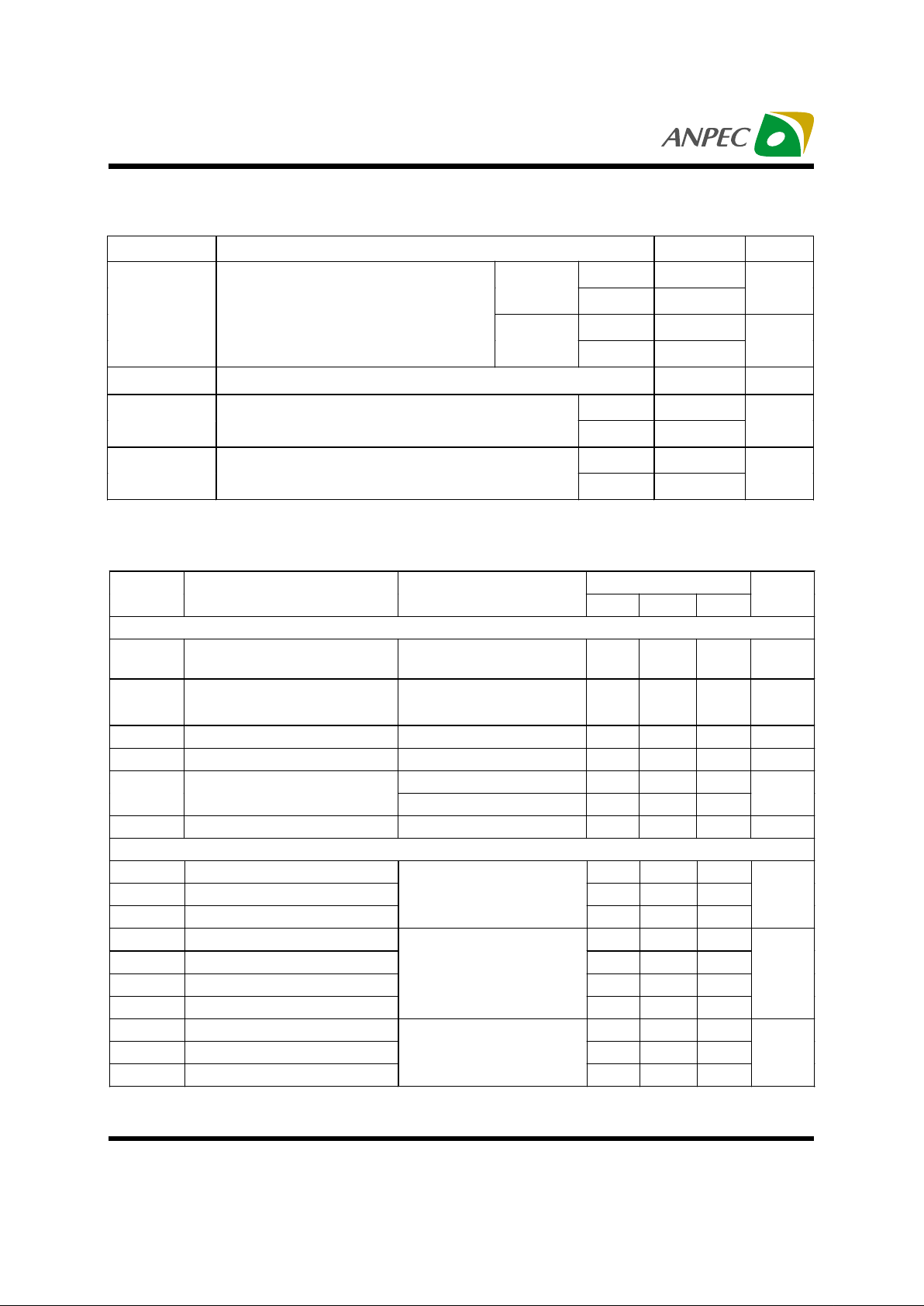
Typical Characteristics (Cont.)
Gate Charge
QG-T otal Gate Charge (nC)
V
GS
-Gate-to-Source Voltage (V)
VDS=15V
IDS=80A
0246810
0.000
0.005
0.010
0.015
0.020
0.025
IDS=60A
VGS-Gate-to-Source Voltage (V)
On-Resistance vs. Gate-to-Source Voltage
R
DS (ON)
-On-Resistance (Ω)
Tj-Junction T emperature (°C)
On-Resistaence vs. Junction T emperature
R
DS(ON)
-On Resistance (mΩ)
VGS=10V
IDS=60A
-50 -25 0 25 50 75 100 125 150
0
2
4
6
8
10
Tj-Junction T emperature (°C)
On-Resistaence vs. Junction T emperature
R
DS(ON)
-On Resistance (mΩ)
(Normalized)
VGS=10V
IDS=60A
Page 5

Copyright ANPEC Electronics Corp.
Rev. A.3 - Jan., 2003
APM3005N
www.anpec.com.tw5
10
-5
10
-4
10
-3
10
-2
10
-1
10
0
0
500
1000
1500
2000
2500
3000
10-510-410-310-210-110010
1
0
500
1000
1500
2000
2500
3000
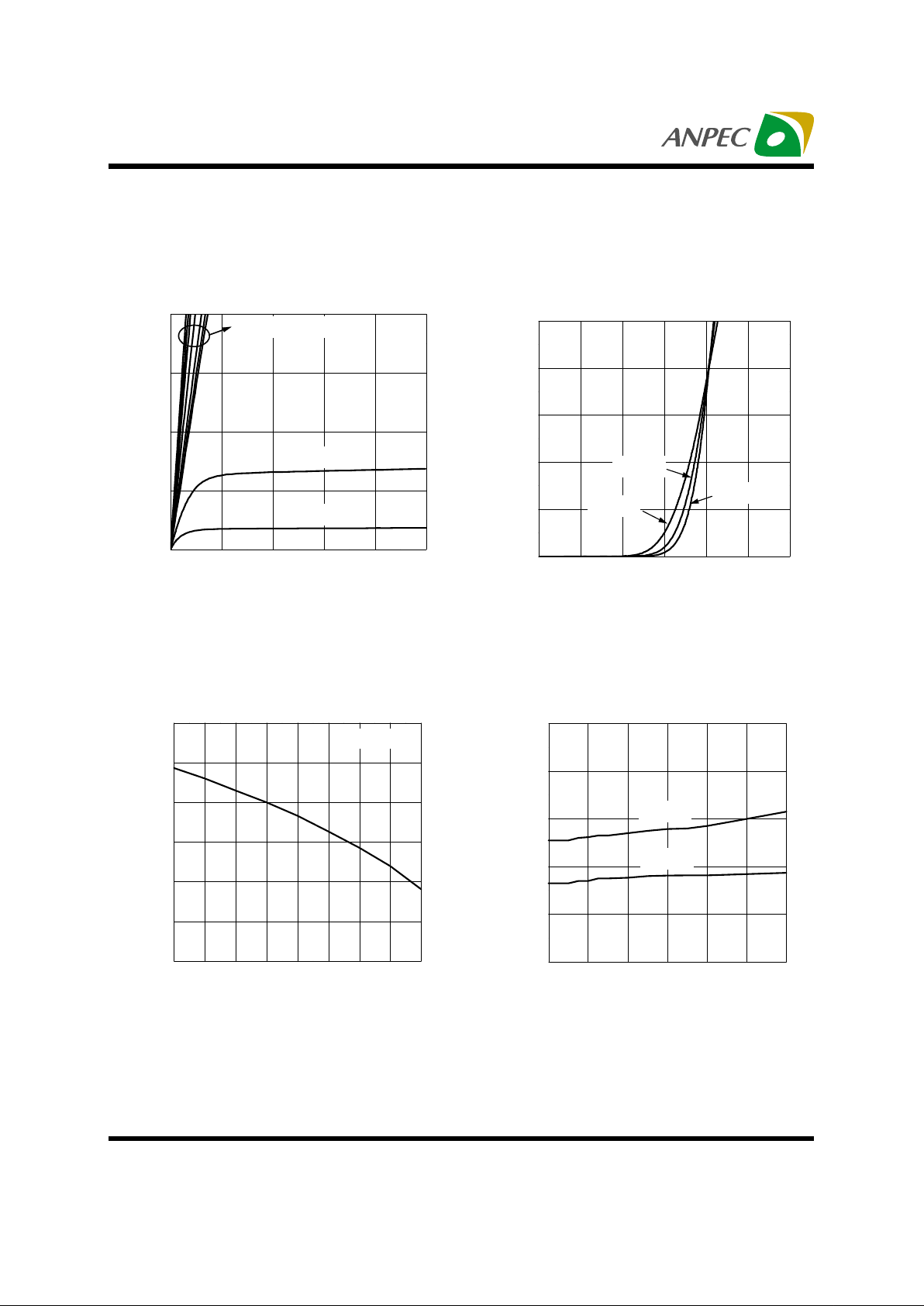
Typical Characteristics (Cont.)
0.0 0.3 0.6 0.9 1.2 1.5
0.1
1
10
100
Source-Drain Diode Forward V oltage
I
SD
-Source Current (A)
VSD-Source-to-Drain Voltage (V)
TJ=-55°C
TJ=25°C
TJ=125°C
0 5 10 15 20 25 30
0
1000
2000
3000
4000
5000
6000
7000
Capacitance Characteristics
VDS-Drain-to-Source Voltage (V)
C-Capacitance (pF)
Crss
Coss
Ciss
Time (sec)
Single Pulse Power
Power (W)
TO-263
Time (sec)
Single Pulse Power
Power (W)
TO-252
Frequency=1MHz
Page 6

Copyright ANPEC Electronics Corp.
Rev. A.3 - Jan., 2003
APM3005N
www.anpec.com.tw6
10
-5
10
-4
10
-3
10
-2
10
-1
10
0
0.01
0.1
1
10
-5
10
-4
10
-3
10
-2
10
-1
10
0
10
1
0.01
0.1
1
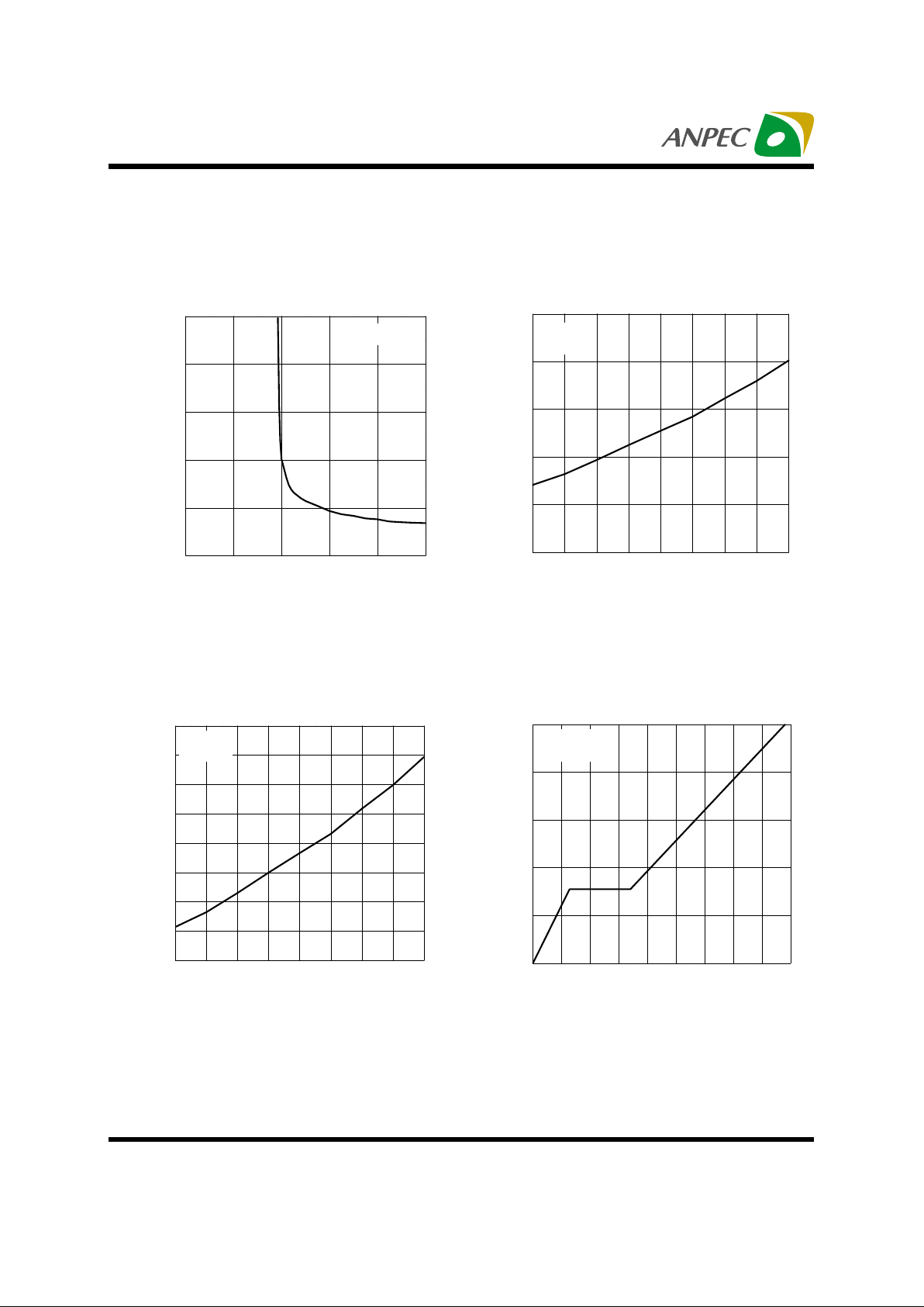
Typical Characteristics (Cont.)
Square Wave Pulse Duration (sec)
Normalized Transient Thermal Transient Impedence, Junction to Ambient
D=0.1
Square Wave Pulse Duration (sec)
Normalized Effective Transient
Thermal Impedance
Normalized Transient Thermal Transient Impedence, Junction to Ambient
1. Duty Cycle , D=t1/t2
2. Per Unit Base=R
thJA
=62.5°C/W
3. TJM-TA=PDMZ
thJA
SINGLE PULSE
D=0.01
D=0.02
D=0.05
D=0.1
D=0.2
Duty Cycle=0.5
TO-263
Normalized Effective Transient
Thermal Impedance
1. Duty Cycle , D=t1/t2
2. Per Unit Base=R
thJA
=50°C/W
3. TJM-TA=PDMZ
thJA
SINGLE PULSE
D=0.01
D=0.02
D=0.05
D=0.2
Duty Cycle=0.5
TO-252
Page 7

Copyright ANPEC Electronics Corp.
Rev. A.3 - Jan., 2003
APM3005N
www.anpec.com.tw7
Package Information
TO-220 ( Reference JEDEC Registration TO-220)
Q
D
R
E
F
J1
e
e1
b1
L1
A
c
b
H1
L
Millimeters Inches
Dim
Min. Max. Min. Max.
A 3.56 4.83 0.140 0 .19 0
b1 1.14 1.78 0.045 0.070
b 0.51 1.14 0.020 0.045
c 0.31 1.14 0.012 0.045
D 14.23 16.51 0.560 0.650
e 2.29 2.79 0.090 0.110
e1 4.83 5.33 0.190 0.210
E 9.65 10.67 0.380 0.420
F 0.51 1.40 0.02 0 0.055
H1 5.84 6.86 0.230 0.270
J1 2.03 2.92 0.080 0.115
L 12.7 14.73 0.500 0.580
L1 3.65 6.35 0.143 0.250
R 3.53 4.09 0.139 0.1 6 1
Q 2.54 3.43 0 .100 0.135
Page 8

Copyright ANPEC Electronics Corp.
Rev. A.3 - Jan., 2003
APM3005N
www.anpec.com.tw8
Package Informaion (Cont.)
TO-252( Reference JEDEC Registration TO-252)
Millimeters Inches
Dim
Min. Max. Min. Max .
A 2.18 2.39 0.086 0.094
A1 0.89 1.27 0.035 0.050
b 0.508 0.89 0.0 20 0.035
b2 5.207 5.4 61 0.205 0.215
C 0.46 0.58 0.018 0.023
C1 0.46 0.58 0.018 0.023
D 5.334 6.2 2 0.210 0.245
E 6.35 6.73 0.250 0.265
e1 3.96 5.18 0. 156 0.204
H 9.398 10.41 0.370 0.410
L 0.51 0.020
L1 0.64 1.02 0. 025 0.040
L2 0.89 2.032 0. 035 0.080
L2
D
L1
b
b2
E
C1
A
H
L
C
A1
e1
Page 9

Copyright ANPEC Electronics Corp.
Rev. A.3 - Jan., 2003
APM3005N
www.anpec.com.tw9
TO-263 ( Reference JEDEC Registration TO-263)
Millimeters Inches
Dim
Min. Max. Min. Max.
A
4.06 4.83
0.160 0.190
b 0.51 1.016 0.02 0.040
b2 1.14 1.651 0.045 0.065
c
0.38 TYP.
0.015 TYP.
c2 1.14 1.40 0.045 0.055
D 8.64 9.65 0.340 0.380
E
9.65 10.54
0.380 0.415
L 14.60 15.88 0.575 0.625
L1 2.24 2.84 0.090 0.110
L2
1.02 2.92
0.040 0.112
L3 1.20 1.78 0.050 0.070
E
D
L
L2
L3
D1
E1
TERMINAL 4
c
A
c2
R
L1
L4
Φ 1
DETAIL "A"ROTED
Package Information (Cont.)
Page 10

Copyright ANPEC Electronics Corp.
Rev. A.3 - Jan., 2003
APM3005N
www.anpec.com.tw10
Reference JEDEC Standard J-STD-020A APRIL 1999
Reflow Condition (IR/Convection or VPR Reflow)
Physical Specifications
Pre-heat temperature
183 C
Peak temperature
Time
°
temperature
Convection or IR/
Convection
VPR
Average ramp-up rate(183°C to Peak) 3°C/second max. 10°C /second max.
Preheat temperature 125± 25°C)
120 seconds max.
Temperature maintained above 183
°
C
60 ~ 150 seconds
Time within 5°C of actual peak temperature
10 ~ 20 seconds
60 seconds
Peak temperature range
220 +5/-0
°
C or 235 +5/-0°C 215~ 219°C or 235 +5/-0°C
Ramp-down rate
6
°
C /second max. 10°C /second max.
Time 25°C to peak temperature
6 minutes max.
pkg. thickness
≥≥≥≥
2.5mm
and all bags
pkg. thickness < 2.5mm and
pkg. volume
≥≥≥≥
350 mm
pkg. thickness < 2.5mm and pkg.
volume <
Convection 220 +5/-0°C
Convection 235 +5/-0
°
C
VPR 215-219°C
VPR 235 +5/-0
°
C
IR/Convection 220 +5/-0
°
C IR/Convection 235 +5/-0
°
C
Classification Reflow Profiles
Package Reflow Conditions
Terminal Material Solder-Plated Copper (Solder Material : 90/10 or 63/37 SnPb)
Lead Solderab ility M eets E IA S pec ification RSI8 6-91 , AN SI/J-ST D- 00 2 C atego ry 3.
Page 11

Copyright ANPEC Electronics Corp.
Rev. A.3 - Jan., 2003
APM3005N
www.anpec.com.tw11
Application
A B C J T1 T2 W P E
330 ±3 100 ± 2 13 ± 0. 5 2 ± 0.5
16.4 + 0.3
-0.2
2.5± 0.5
16+ 0.3
- 0.1
8 ± 0.1 1.75± 0.1
F D D1 Po P1 Ao Bo Ko t
TO-252
7.5 ± 0.1 1.5 +0.1 1.5± 0.25 4.0 ± 0.1 2.0 ± 0.1 6.8 ± 0.1 10.4± 0.1 2.5± 0.1 0.3±0.05
Application
A B C J T1 T2 W P E
380±3 80 ± 2 13 ± 0. 5 2 ± 0.5 24 ± 42± 0.3
24 + 0.3
- 0.1
16 ± 0.1 1.75± 0.1
F D D1 Po P1 Ao Bo Ko t
TO-263
11.5 ± 0.1
1.5 +0.1
1.5± 0.25 4.0 ± 0.1 2.0 ± 0.1 10.8 ± 0.1 16.1± 0.1 5.2± 0.1 0.35±0.013
(mm)
A
J
B
T2
T1
C
t
Ao
E
W
Po
P
Ko
Bo
D1
D
F
P1
Carrier Tape & Reel Dimension
Test item Method Description
SOLDERABILITY MIL-STD-883D-2003 245°C,5 SEC
HOLT MIL-STD 883D-1005.7 1000 Hrs Bias @ 125°C
PCT JESD-22-B, A102 168 Hrs, 100% RH, 121°C
TST MIL-STD 883D-1011.9 -65°C ~ 150°C, 200 Cycles
Reliability test program
Page 12

Copyright ANPEC Electronics Corp.
Rev. A.3 - Jan., 2003
APM3005N
www.anpec.com.tw12
Cover Tape Dimensions
Customer Service
Anpec Electronics Corp.
Head Office :
5F, No. 2 Li-Hsin Road, SBIP,
Hsin-Chu, T aiwan, R.O.C.
T el : 886-3-5642000
Fax : 886-3-5642050
Taipei Branch :
7F, No. 137, Lane 235, Pac Chiao Rd.,
Hsin Tien City, Taipei Hsien, Taiwan, R. O. C.
T el : 886-2-89191368
Fax : 886-2-89191369
Application Carrier Width Cover Tape Width Devices Per Reel
TO- 252
16 13.3 2500
TO- 263
24 21.3 1000
 Loading...