

Page 1
APM2506NU
y
g
A
Features
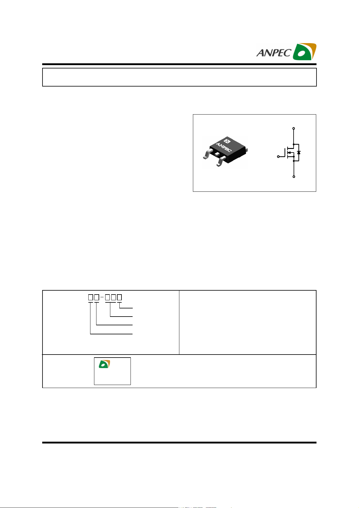
N-Channel Enhancement Mode MOSFET
Pin Description
z 25V/60A,
R
= 5mΩ (typ.) @ VGS= 10V
DS(ON)
= 7mΩ (typ.) @ VGS= 4.5V
R
DS(ON)
z Super High Dense Cell Design
z Avalanche Rated
z Reliable and Rugged
3
1
2
Applications
z Power Management in Desktop Computer or
DC/DC Converters
Ordering and Marking Information
Pin 3
D
Pin 1
G
S
Pin 2
PM2506N
APM2506N U:
APM2506N
XXXXX
Lead Free Code
Handing Code
Temp. Range
Package Code
Package Code
U : TO-252
Operating Junction Temp. Range
C : -55 to 150°C
Handling Code
TU : Tube TR : Tape & Reel
Lead Free Code
L : Lead Free Device
Blank : Original Device
XXXXX – Date Code
ANPEC reserves the right to make changes to improve reliability or manufacturability without notice, and advise
customers to obtain the latest version of relevant information to verif
Copyright©ANPEC Electronics Corp.
Rev. B.1 - Oct., 2003
1
before placin
orders.
www.anpec.com.tw
Page 2

APM2506NU
Absolute Maximum Ratings
Symbol
Common Ratings (TA = 25°C)
V
DSS
V
GSS
TJ
T
STG
Drain-Source Voltage
Gate-Source Voltage
Maximum Junction Temperature
Storag e Temperature Range -55 to 150
Mounted on Large Heat Sink
R
IDP
ID
PD
θJC
300µs Pulse Drain Current Tested
Continuous Drain Current
Maximum Power Dissipation
Thermal Resistance-Junction to Case
Mounted on PCB of 1in2 pad
R
IDP
ID
PD
θJA
300µs Pulse Drain Current Tested
Continuous Drain Current
Maximum Power Dissipation
Thermal Resistance-Junction to Ambient 50 °C/W
area
Parameter Rating Unit
±25
±20
150
TC=25°C 150
T
=100°C 80
C
TC=25°C 60*
=100°C 40
T
C
TC=25°C
=100°C
T
C
50
20
2.5
°C/W
TA=25°C 150
=100°C 80
T
A
TA=25°C 17
=100°C 10
T
A
TA=25°C
=100°C
T
A
2.5
1
V
°C
°C
A
A
W
A
A
W
Mounted on PCB of Minimum Footprint
IDP
ID
PD
R
θJA
Notes:
* Current limited by bond wire
Copyright©ANPEC Electronics Corp.
Rev. B.1 - Oct., 2003
300µs Pulse Drain Current Tested
Continuous Drain Current
Maximum Power Dissipation
Thermal Resistance-Junction to Ambient 75 °C/W
2
TA=25°C 150
=100°C 80
T
A
TA=25°C 13
T
=100°C 7
A
TA=25°C
=100°C
T
A
1.5
0.5
www.anpec.com.tw
A
A
°C/W
°C/W
Page 3
APM2506NU
Electrical Characteristics (T
Symbol Parameter Test Condition
Drain-Source Avalanche Ratings
EAS Drain-Source Avalanche Energy ID=45A, VDD=15V 100 mJ
Static
BV
Drain-Source Breakdown Voltage
DSS
I
Zero Gate Voltage Drain Current VDS=20V, VGS=0V 1
DSS
V
Gate Threshold Voltage
GS(th)
I
Gate Leakage Current VGS=±20V, VDS=0V ±100 nA
GSS
a
R
Diode
Drain-Source On-state Resistance
DS(ON)
a
V
Diode Forward Voltage ISD=20A , VGS=0V 0.7 1.3 V
SD
IS Diode continuous forward current TA=25°C 40 A
=25°C)
A
APM2506NU
Unit
Min. Typ. Max.
V
=0V, IDS=250µA
GS
25 V
µA
V
DS=VGS
, IDS=250µA
1 1.5 2 V
VGS=10V, IDS=40A 5 6
mΩ
V
=4.5V, IDS=20A 7 10
GS
Dynamicb
C
Input Capacitance 3000 pF
iss
C
Output Capacitance 670 pF
oss
C
Reverse Transfer Capacitance
rss
t
Turn-on Delay Time 13 20 ns
d(ON)
Tr Turn-on Rise Time 9 15 ns
t
Turn-off Delay Time 43 66 ns
d(OFF)
Tf Turn-off Fall Time
V
=0V
GS
=15V
V
DS
Frequency=1.0MHz
V
=15V, R
DD
IDS=1A, V
R
=6Ω
G
GEN
=15Ω
L
=10V,
360 pF
14 28 ns
Gate Chargeb
Qg Total Gate Charge 32 42 nC
=15V, VGS=4.5V,
V
Qgs Gate-Source Charge 6.6 nC
Qgd Gate-Drain Charge
Notes:
a : Pulse test ; pulse width≤300
b : Guaranteed by design, not subject to production testing
µs, duty cycle≤2%
I
DS
DS
=20A
12.4 nC
Copyright©ANPEC Electronics Corp.
Rev. B.1 - Oct., 2003
3
www.anpec.com.tw
Page 4
APM2506NU
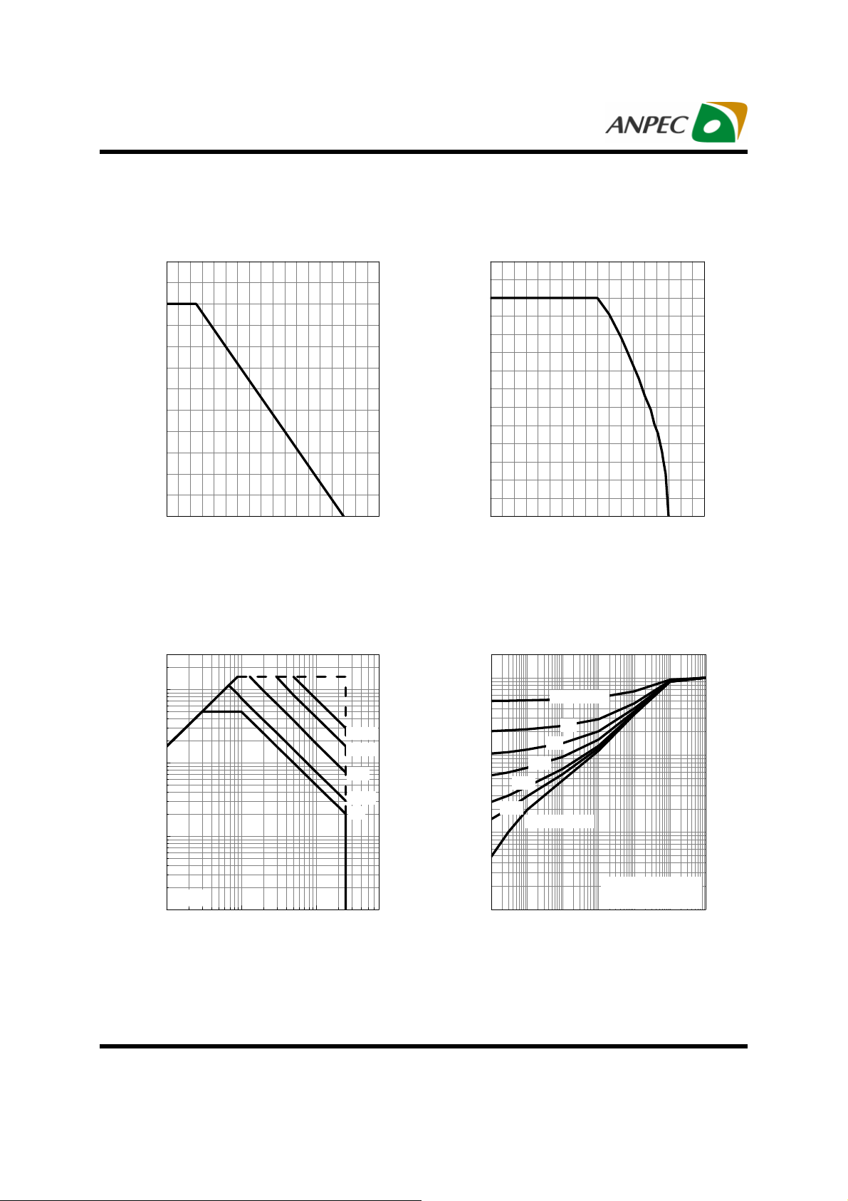
Typical Characteristics
Power Dissipation
60
70
Drain Current
50
40
30
- Power (W)
tot
20
P
10
0
0 20 40 60 80 100 120 140 160 180
Tj - Junction Temperature (°C)
Safe Operation Area
300
100
60
50
40
30
20
- Drain Current (A)
D
I
10
0
0 20 40 60 80 100 120 140 160 180
Tj - Junction Temperature (°C)
Thermal Transient Impedance
1
Duty = 0.5
100µs
10
1
- Drain Current (A)
D
I
300µs
1ms
10ms
DC
0.1
0.02
0.01
0.01
0.2
0.1
0.05
Single Pulse
Normalized Effective Transient
TC=25OC
0.1
0.1 1 10 70
V
- Drain-Source Voltage (V) Square Wave Pulse Duration (sec)
DS
Copyright©ANPEC Electronics Corp.
Rev. B.1 - Oct., 2003
1E-3
1E-4 1E-3 0.01 0.1 1 10 100
4
Mounted on 1i n2 pad
:50oC/W
R
θJA
www.anpec.com.tw
Page 5

APM2506NU
Typical Characteristics
100
Output Characteristics
Drain-Source On Resistance
12
VGS=3.5,4,5,6,7,8,9,10V
80
60
3V
40
- Drain Current (A)
D
I
20
0
0246810
V
- Drain-Source Voltage (V)
DS
2.5V
2V
10
8
6
4
- On Resistance (mΩ)
DS(ON)
2
R
0
0 20406080100
ID - Drain Current (A)
100
80
Transfer Characteristics
Gate Threshold Voltage
1.6
1.4
1.2
VGS=4.5V
VGS=10V
IDS =250µA
60
Tj=125oC
40
- Drain Current (A)
D
I
Copyright©ANPEC Electronics Corp.
Rev. B.1 - Oct., 2003
Tj=25oC
20
0
012345
V
- Gate-Source Voltage (V)
GS
Tj=-55oC
5
1.0
0.8
0.6
0.4
0.2
Normalized Threshold Voltage
0.0
-50 -25 0 25 50 75 100 125 150
T
- Junction Temperature (°C)
j
www.anpec.com.tw
Page 6

APM2506NU
Typical Characteristics
Drain-Source On Resistance
2.00
VGS = 10V
= 40A
I
1.75
DS
Source-Drain Diode Forward
100
1.50
1.25
1.00
0.75
0.50
Normalized On Resistance
0.25
0.00
-50 -25 0 25 50 75 100 125 150
Tj - Junction Temperature (°C)
RON@Tj=25oC: 5mΩ
10
- Source Current (A)
1
S
0.0 0.2 0.4 0.6 0.8 1.0 1.2 1.4 1.6
Tj=150oC
VSD - Source-Drain Voltage (V)
6000
5000
4000
3000
2000
C - Capacitance (nC)
1000
0
0 5 10 15 20 25
VDS - Drain-Source Voltage (V)
Capacitance
Frequency=1MHz
Ciss
Coss
Crss
Gate Charge
0
VDS=10 V
9
= 30 A
I
D
8
7
6
5
4
3
- Gate-Source Voltage (V) I
2
GS
V
1
0
0 10203040506070
QG - Gate Charge (nC)
Tj=25oC
Copyright©ANPEC Electronics Corp.
Rev. B.1 - Oct., 2003
6
www.anpec.com.tw
Page 7

APM2506NU
Avalanche Test Circuit and Waveforms
VDS
L
DUT
IAS
RG
VDD
VDSX(SUS)
tp
VDS
tp
IL
0.01Ω
Switching Time Test Circuit and Waveforms
VDS
RD
DUT
VGS
RG
VDD
VDS
90%
VDD
EAS
tAV
tp
10%
VGS
td(on) tr
Copyright©ANPEC Electronics Corp.
Rev. B.1 - Oct., 2003
7
td(off) tf
www.anpec.com.tw
Page 8

APM2506NU
Package information
E
b2
L2
D
L1
A
C1
H
L
b
e1
C
A1
Dim
A 2.18 2.39 0.086 0.094
A1 0.89 1.27 0.035 0.050
b 0.508 0.89 0.020 0.035
b2 5.207 5.461 0.205 0.215
C 0.46 0.58 0.018 0.023
C1 0.46 0.58 0.018 0.023
D 5.334 6.22 0.210 0.245
E 6.35 6.73 0.250 0.265
e1 3.96 5.18 0.156 0.204
H 9.398 10.41 0.370 0.410
L 0.51 0.020
L1 0.64 1.02 0.025 0.040
L2 0.89 2.032 0.035 0.080
Millimeters Inches
Min. Max. Min. Max.
Copyright©ANPEC Electronics Corp.
Rev. B.1 - Oct., 2003
8
www.anpec.com.tw
Page 9

APM2506NU
Physical Specifications
Terminal Material Solder-Plated Copper (Solder Material : 90/10 or 63/37 SnPb)
Lead Solderability Meets EIA Specification RSI86-91, ANSI/J-STD-002 Category 3.
Reflow Condition
(IR/Convection or VPR Reflow)
Peak temperature
temperature
Pre-heat temperature
°
183 C
Classification Reflow Profiles
Average ramp-up rate (183°C to Peak) 3°C/ second max. 10°C /second max.
Preheat temperature (125 ± 25°C)
Temperature maintained above 183°C
Time within 5°C of actual peak temperature
Peak temperature range
Ramp-down rate
Time 25°C to peak temperature
Convection or IR/
Convection
120 seconds max.
60~150 seconds
10~20 seconds 60 seconds
220 + 5/-0
°C /second max. 10°C /second max.
6
6 minutes max.
°C or 235 +5°C/-0°C 215~ 219 °C or 235 +5°C/-0°C
VPR
Time
Copyright©ANPEC Electronics Corp.
Rev. B.1 - Oct., 2003
9
www.anpec.com.tw
Page 10

APM2506NU
Reliability test program
Test item Method Description
SOLDERABILITY MIL-STD-883D-2003 245°C,5 SEC
HOLT MIL-STD 883D-1005.7 1000 Hrs Bias @125°C
PCT JESD-22-B, A102 168 Hrs, 100% RH, 121°C
TST MIL-STD 883D-1011.9 -65°C ~ 150°C, 200 Cycles
Carrier Tape & Reel Dimension
t
D
D1
T2
T1
Bo
Ko
B
W
A
E
F
Po
J
P
P1
Ao
C
Application
TO-252
A B C J T1 T2 W P E
330±3 100±2 13±0.5 2±0.5
F D D1 Po P1 Ao Bo Ko t
7.5±0.1 1.5±0.1 1.5±0.25 4.0±0.1 2.0±0.1 6.8±0.1 10.4±0.1 2.5±0.1 0.3±0.05
16.4+0.3
-0.2
2.5±0.5
16+0.3
16-0.1
8±0.1 1.75±0.1
(mm)
Copyright©ANPEC Electronics Corp.
Rev. B.1 - Oct., 2003
10
www.anpec.com.tw
Page 11

APM2506NU
Cover Tape Dimensions
Application Carrier Width Cover Tape Width Devices Per Reel
TO-252 16 13.3 2500
Customer Service
Anpec Electronics Corp.
Head Office :
5F, No. 2 Li-Hsin Road, SBIP,
Hsin-Chu, Taiwan, R.O.C.
Tel : 886-3-5642000
Fax : 886-3-5642050
Taipei Branch :
7F, No. 137, Lane 235, Pac Chiao Rd.,
Hsin Tien City, Taipei Hsien, Taiwan, R. O. C.
Tel : 886-2-89191368
Fax : 886-2-89191369
Copyright©ANPEC Electronics Corp.
Rev. B.1 - Oct., 2003
11
www.anpec.com.tw
 Loading...