

Page 1
APM2054N
N-Channel Enhancement Mode MOSFET
Features
• 20V/12A, R
R
R
••
•
Super High Dense Cell Design
••
••
•
High Power and Current Handling Capability
••
••
•
TO-252, SOT-89 and SOT-223 Packages
••
=35mΩ(typ.) @ VGS=10V
DS(ON)
=45mΩ(typ.) @ VGS=4.5V
DS(ON)
=110mΩ(typ.) @ VGS=2.5V
DS(ON)
Pin Description
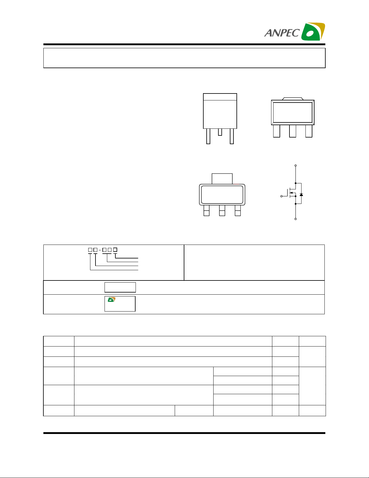
Top View of TO-252
Applications
• Switching Regulators
• Switching Converters
Top View of SOT-223
Ordering and Marking Information
APM2054N
AP M 2054N D /V :
APM2054N
XXXXX
Lead Free Code
Handling Code
Tem p R ange
Package C ode
Package C ode
Package C ode
D : S O T-89 V : SO T-223 U : TO-252
Operation Junction Tem p. Range
C : -55 to 150 C
Handling Code
TR : Tape & Reel
Lead Feed C ode
L : Lead Free D evice B lank : Original Device
XXXXX - Date Code
123
GDS
123
SDG
°
°
123
GDS
Top View of SOT-89
D
G
S
N-Channel MOSFET
AP M 2054N U :
APM2054N
XXXXX
Absolute Maximum Ratings (T
XXXXX - Date Code
= 25°C unless otherwise noted)
A
Symbol Parameter Rating Unit
V
DSS
V
GSS
ID*
IDM
PD*
ANPEC reserves the right to make changes to improve reliability or manufacturability without notice, and advise
customers to obtain the latest version of relevant information to verify before placing orders.
Copyright ANPEC Electronics Corp.
Rev. A.3 - Nov., 2003
Drain-Source Voltage 20
Gate-Source Voltage ±16
Maximum Drain Current – Continuous
Maximum Drain Current – Pulsed
Maximum Power Dissipation
T
=25°C TO-252 5 W
A
TO-252
SOT-223/SO T-89
TO-252 25
SOT-223/SO T-89
V
10
4
A
12
www.anpec.com.tw1
Page 2
APM2054N
Absolute Maximum Ratings (T
= 25°C unless otherwise noted)
A
Symbol Parameter Rating Unit
TA=25°C SOT-223/SOT-89 1.25
PD*
TJ
T
STG
Maximum Power Dissipation
T
=100°C
A
TO-252
SOT-223/SOT-89 0.5
Maximum Junction Temperature
Storage Temperature Range -55 to 150 °C
2
150 °C
W
* Surface Mounted on FR4 Board, t ≤ 10 sec.
Electrical Characteristics (TA=25°C unless otherwise noted)
Symbol Parameter Test Condition
APM2054N
Min. Typ. Max.
Unit
Static
BV
Drain-Source Breakdown Voltage
DSS
I
Zero G ate Voltage Drain Current VDS=16V, VGS=0V 1
DSS
V
Gate Threshold Voltage
GS(th)
I
Gate Leakage Current
GSS
V
=0V, IDS=250µA
GS
V
DS=VGS
V
GS
, IDS=250µA
=±16V, VDS=0V
20 V
µA
0.7 0.9 1.5 V
±100
nA
VGS=10V, IDS=12A 35 40
R
Drain-Source O n-state Resistance
DS(ON)
VGS=4.5V, IDS=6A 45 54
V
=2.5V, IDS=2A 110 130
GS
mΩ
VSD Diode Forward Voltage ISD=6A, VGS=0V 0.7 1.3 V
Dynamic
Qg Total Gate Charge 11 13
V
=10V, VGS=4.5V,
Qgs Gate-Source Charge 3.8
Qgd Gate-Drain Charge
t
Turn-on Delay Time 12 24
d(ON)
tr Turn-on Rise Tim e 10 20
t
Turn-off Delay Tim e 40 74
d(OFF)
tf Tu rn-o ff F a ll Tim e
C
Input Capacitance 450
iss
C
Output Capacitance 100
oss
C
Reverse Transfer Capacitance
rss
Notes
a
: Pulse test ; pulse width ≤300µs, duty cycle ≤ 2%
b
: Guaranteed by design, not subject to production testing
Copyright ANPEC Electronics Corp.
Rev. A.3 - Nov., 2003
DS
I
=6A
DS
=10V, IDS=1A,
V
DD
=4.5V, RG=6Ω
V
GEN
V
=0V
GS
V
=15V
DS
Frequency=1.0MHz
5.2
20 38
60
www.anpec.com.tw2
nC
ns
pF
Page 3
APM2054N
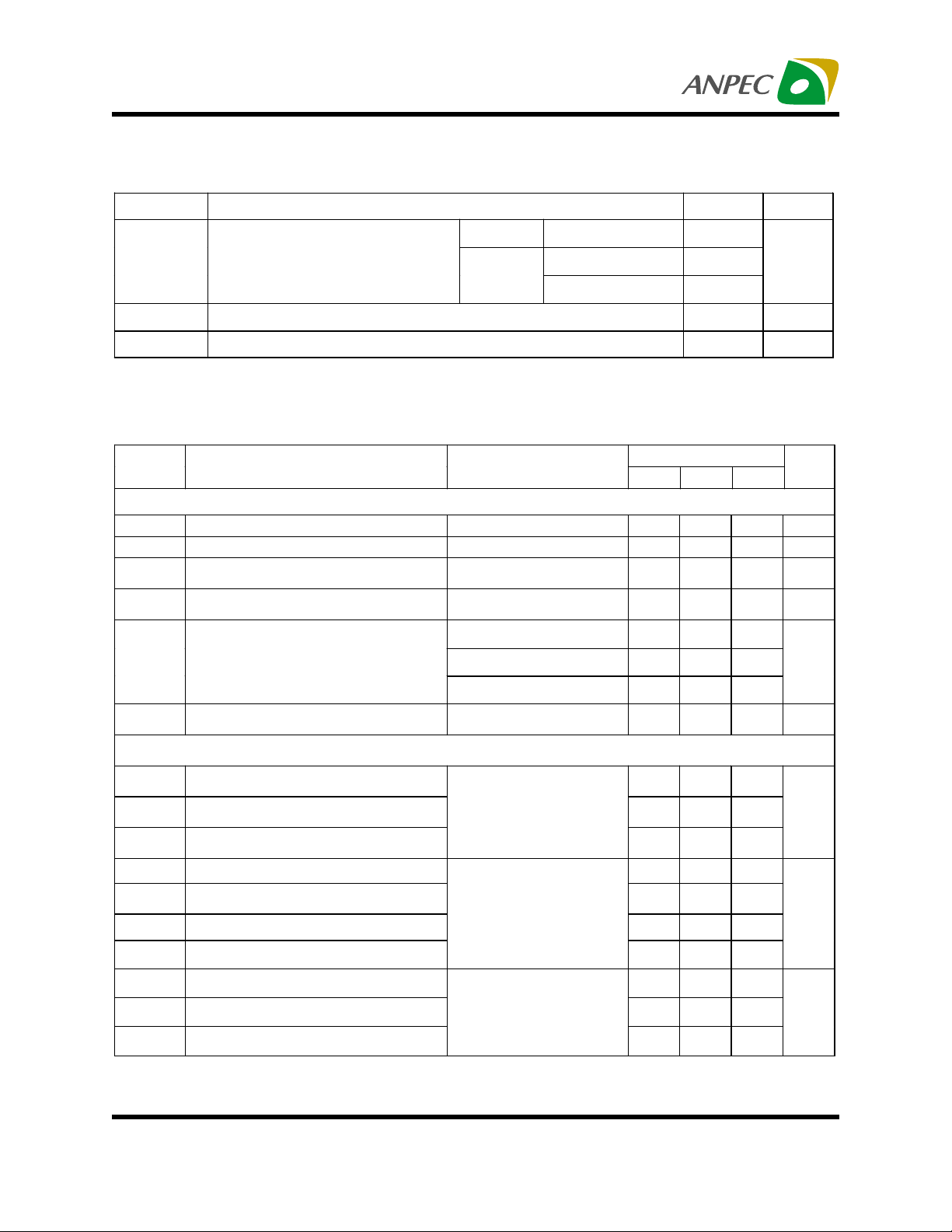
Typical Characteristics
Output Characteristics
12
9
6
ID-Drain Current (A)
3
0
0246810
VGS= 4, 5, 6, 7, 8, 9, 10V
VGS=3V
VGS=2V
VDS - Drain-to-Source V oltage (V)
Threshold Voltage vs. Temperature
1.50
1.25
IDS=250uA
Transfer Characteristics
12
9
6
ID-Drain Current (A)
3
0
012345
Tj=25oC
Tj=125oC
Tj=-55oC
VGS - Gate-to-Source V oltage (V)
On-Resistance vs. Drain Current
0.07
0.06
1.00
0.75
(Normalized)
0.50
0.25
VGS(th)-Threshold Voltage (V)
0.00
-50 -25 0 25 50 75 100 125 150
Tj - Junction T emperature (°C)
Copyright ANPEC Electronics Corp.
Rev. A.3 - Nov., 2003
0.05
0.04
0.03
RDS(ON)-On-Resistance (Ω)
0.02
0.01
0246810
VGS=10V
VGS=4.5V
ID - Drain Current (A)
www.anpec.com.tw3
Page 4
APM2054N
Typical Characteristics
On-Resistance vs. Gate-to-Source Voltage
0.10
0.08
0.06
0.04
0.02
RDS(ON)-On-Resistance (Ω)
0.00
0246810
ID= 6A
VGS - Gate-to-Source V oltage (V)
On-Resistance vs. Junction T emperature
0.07
VGS=10V
ID=12A
0.06
0.05
On-Resistance vs. Junction T emperature
2.00
VGS=10V
ID=12A
1.75
1.50
1.25
1.00
0.75
(Normalized)
0.50
RDS(ON)-On-Resistance (Ω)
0.25
0.00
-50 -25 0 25 50 75 100 125 150
TJ - Junction Temperature (°C)
Gate Charge
10
VDS=10V
ID=6A
8
0.04
0.03
0.02
RDS(ON)-On-Resistance (Ω)
0.01
0.00
-50 -25 0 25 50 75 100 125 150
TJ - Junction Temperature (°C)
Copyright ANPEC Electronics Corp.
Rev. A.3 - Nov., 2003
6
4
2
VGS-Gate-Source Voltage (V)
0
0 5 10 15 20 25
QG -Total Gate Charge (nC)
www.anpec.com.tw4
Page 5
APM2054N
Typical Characteristics
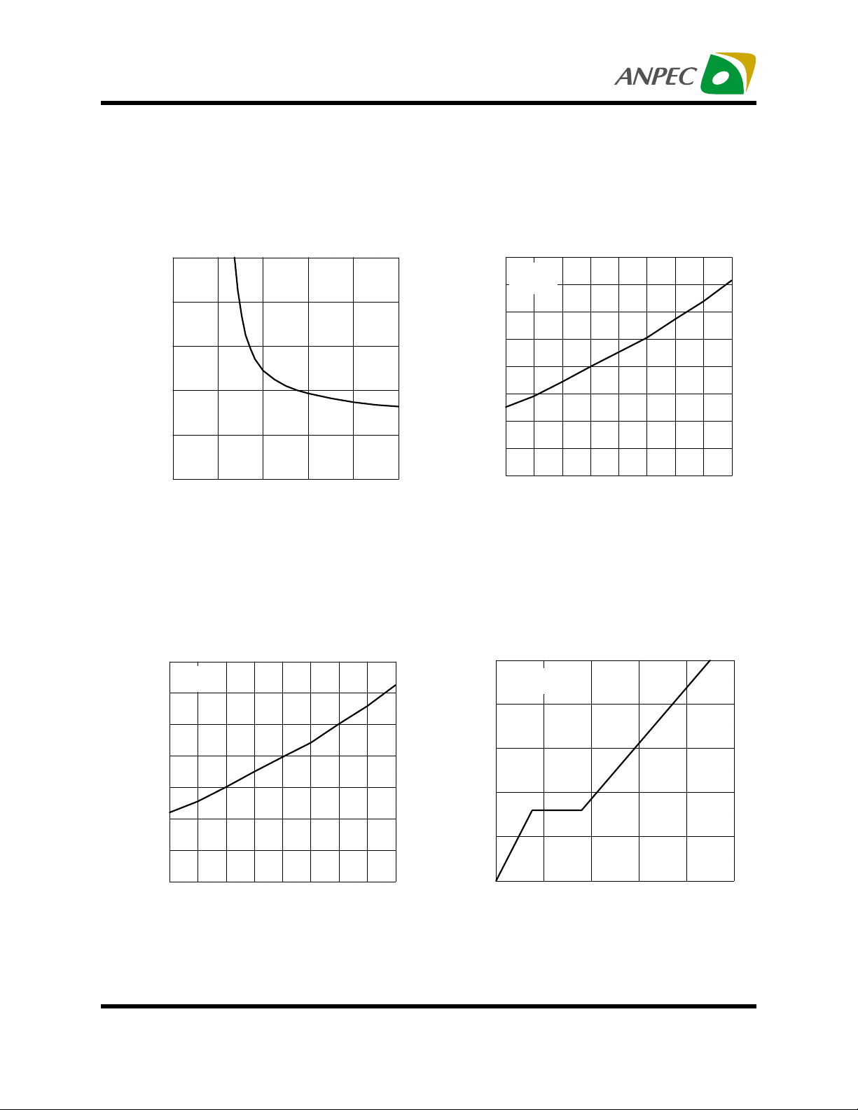
Capacitance
750
625
500
375
250
Capacitance (pF)
125
0
0 5 10 15 20
VDS - Drain-to-Source Voltage (V)
Single Pulse Power
150
Frequency=1MHz
Ciss
Coss
Crss
TO-252
Source-Drain Diode Forward V oltage
12
10
TJ=150°C TJ=25°C
IS-Source Current (A)
1
0.0 0.2 0.4 0.6 0.8 1.0 1.2 1.4 1.6 1.8 2.0
VSD -Source-to-Drain V oltage (V)
Single Pulse Power
350
SOT-223/89
120
90
60
Power (W)
30
0
1E-4 1E-3 0.01 0.1 1 10 100
Time (sec)
Copyright ANPEC Electronics Corp.
Rev. A.3 - Nov., 2003
300
280
210
140
Power (W)
70
0
1E-4 1E-3 0.01 0.1 1 10 100
300
Time (sec)
www.anpec.com.tw5
Page 6

APM2054N
Typical Characteristics
Normalized Thermal Transient Impedence, Junction to Ambient
2
1
Duty Cycle=0.5
D=0.2
0.1
D=0.1
D=0.05
D=0.02
0.01
Thermal Impedance
SINGLE PULSE
Normalized Effective Transient
1E-3
1E-4 1E-3 0.01 0.1 1 10 100 300
Normalized Thermal Transient Impedence, Junction to Ambient
2
1
Square Wave Pulse Duration (sec)
1.Duty Cycle, D= t1/t2
2.Per Unit Base=R
3.TJM-TA=PDMZ
4.Surface Mounted
thJA
thJA
TO-252
=50oC/W
SOT-223/89
Duty Cycle=0.5
D=0.2
0.1
D=0.1
D=0.05
D=0.02
0.01
Thermal Impedance
SINGLE PULSE
Normalized Effective Transient
1E-3
1E-4 1E-3 0.01 0.1 1 10 100 300
Copyright ANPEC Electronics Corp.
Rev. A.3 - Nov., 2003
Square Wave Pulse Duration (sec)
1.Duty Cycle, D= t1/t2
2.Per Unit Base=R
3.TJM-TA=PDMZ
4.Surface Mounted
thJA
thJA
www.anpec.com.tw6
=100oC/W
Page 7

APM2054N
Package Information
TO-252( Reference JEDEC Registration TO-252)
E
b2
A
C1
L2
D
H
L1
L
b
e1
C
A1
Dim
A 2.18 2.39 0.086 0.094
A1 0.89 1.27 0.035 0.050
b 0.508 0.89 0.020 0. 035
b2 5.207 5.4 61 0.205 0.215
C 0.46 0.58 0.018 0.023
C1 0.46 0.58 0.018 0.023
D 5.334 6.22 0.210 0.2 45
E 6.35 6.73 0.250 0.265
e1 3.96 5.1 8 0.156 0.204
H 9.398 10.41 0.370 0.410
L 0.51 0.020
L1 0.64 1.0 2 0.025 0.040
L2 0.89 2.032 0.035 0.080
Copyright ANPEC Electronics Corp.
Rev. A.3 - Nov., 2003
Min. Max. Min. Max .
Millimeters Inches
www.anpec.com.tw7
Page 8

APM2054N
Package Information
SOT-89 (Reference EIAJ ED-7500A Reg stration SC-62)
D
D1
H
L
123
a
E
C
Dim
B1
B
e
e1
A
a
Millimeters Inches
Min. Max. Min. Max.
A 1 .40 1.60 0.055 0.063
B 0 .40 0.56 0.016 0.022
B1 0 .35 0.48 0.014 0.019
C 0.35 0 .44 0 .014 0.017
D 4.40 4 .60 0 .173 0.181
D1 1.35 1 .83 0 .053 0.072
e 1.50 BSC 0.059 BSC
e1 3.00 B SC 0.118 BSC
E 2 .29 2.60 0.090 0.102
H 3.75 4 .25 0 .148 0.167
L 0.80 1.20 0.031 0.047
α
10
°
10
°
Copyright ANPEC Electronics Corp.
Rev. A.3 - Nov., 2003
www.anpec.com.tw8
Page 9

APM2054N
Package Information
SOT-223( Reference JEDEC Registration SOT-223)
D
B1
H E
K
e
e1
B
A
A1
b
a
c
L
Millimeters InchesDim
Min. Max. Min. Max.
A 1.50 1.80 0.06 0.07
A1 0.02 0.08
B 0.60 0.80 0.02 0.03
B1 2.90 3.10 0.11 0.12
c 0.28 0.32 0.01 0.01
D 6.30 6.70 0.25 0.26
E 3.30 3.70 0.13 0.15
e 2.3 BSC 0.09 BSC
e1 4.6 BSC 0.18 BSC
H 6.70 7.30 0.26 0.29
L 0.91 1.10 0.04 0.04
K 1.50 2.00 0.06 0.08
α
β
Copyright ANPEC Electronics Corp.
Rev. A.3 - Nov., 2003
0
°
13
°
10
°
0
°
13
10
°
°
www.anpec.com.tw9
Page 10

APM2054N
Physical Specifications
Terminal Mate rial So lde r-Plated Co p per (S olde r Ma te rial : 90/10 or 63/37 SnPb )
Lead Solderability Meets EIA Specification RSI86-91, ANSI/J-STD-002 Category 3.
Reflow Condition (IR/Convection or VPR Reflow)
Peak temperature
temperature
Pre-heat temperature
°
183 C
Time
Classification Reflow Profiles
Convection or IR/
Convection
Average ramp-up rate(183°C to Peak) 3°C/second max. 10 °C /second max.
Preheat temperature 125 ± 25°C)
Temperature mainta ined abov e 1 83°C
Time within 5°C of actual peak temperature
Peak temperature range
Ramp-down rate
Time 25°C to peak temperature
120 seconds max
60 – 150 seconds
10 –20 seconds 60 seconds
220 +5/-0°C or 235 +5/-0°C 215-219°C or 235 +5/-0°C
6 °C /second max. 10 °C /second max.
6 minutes max.
VPR
Package Re flow Conditions
pkg. thickness ≥≥≥≥ 2.5mm
and all bgas
Convection 220 +5/-0 °C Convection 235 +5/-0 °C
VPR 215-219 °C VPR 235 +5/-0 °C
IR/Convection 220 +5/-0 °C IR/Convection 235 +5/-0 °C
Copyright ANPEC Electronics Corp.
Rev. A.3 - Nov., 2003
pkg. thickness < 2.5mm and
pkg. volume ≥≥≥≥ 350 mm³
pkg. thickness < 2.5mm and pkg.
volume < 350mm³
www.anpec.com.tw10
Page 11

APM2054N
Reflow Condition (IR/Convection or VPR Reflow)
T
P
Ramp-up
T
L
Tsmax
Tsmin
Temperature
ts
Preheat
25
t 25:C to P e a k
tp
t
L
Ramp-down
Critical Zone
T
to T
L
P
Time
Classificatin Reflow Profiles
Profile Feature Sn-Pb Eutectic Assembly Pb-Free Assembly
Large Body Small Body Large Body Small Body
Average ramp-up rate
(T
to TP)
L
Preheat
- Temperature Min (Tsmin)
- Temperature Mix (Tsmax)
- Time (min to max)(ts)
Tsmax to TL
- Temperature(T
- Time (t
L
)
L
)
Peak Temperature(Tp)
Time within 5°C of actual Peak
Temperature(tp)
225 +0/-5°C 240 +0/-5°C 245 +0/-5°C 250 +0/-5°C
Ramp-down Rate 10-30 seconds 10-30 seconds 10-30 seconds 20-40 seconds
Time 25°C to Peak Temperature
6 minutes max. 8 minutes max.
Note: All temperatures refer to topside of the package. Measured on the body surface.
Copyright ANPEC Electronics Corp.
Rev. A.3 - Nov., 2003
3°C/second max. 3°C/second max.
100°C
150°C
60-120 seconds
150°C
200°C
60-180 seconds
3°C/second max
183°C
60-150 seconds
217°C
60-150 seconds
6°C/second max. 6°C/second max.
www.anpec.com.tw11
Page 12

APM2054N
Reliability test program
T est item Method Description
SOLDERABILITY MIL-STD-883D-2003 245°C,5 SEC
HOLT MIL-STD 883D-1005.7 1000 Hrs Bias @ 125°C
PCT JESD-22-B, A102 168 Hrs, 100% RH, 121°C
TST MIL-STD 883D-1011.9 -65°C ~ 150°C, 200 Cycles
Carrier Tape & Reel Dimensions
t
W
E
F
Po
A
P
P1
Ao
J
D
Bo
D1
C
Ko
T2
B
T1
Copyright ANPEC Electronics Corp.
Rev. A.3 - Nov., 2003
www.anpec.com.tw12
Page 13

APM2054N
Application
TO-252
Application
SOT-89
Application
SOT-223
A B C J T1 T2 W P E
330 ±3100 ± 213 ± 0. 5 2 ± 0.5
F D D1 Po P1 Ao Bo Ko t
7.5 ± 0.1 1.5 +0.1 1.5± 0.25 4.0 ± 0.1 2.0 ± 0.1 6.8 ± 0.1 10.4± 0.1 2.5± 0.1 0.3±0.05
A B C J T1 T2 W P E
178 ±170 ± 213.5 ± 0.15 3 ± 0.15 14 ± 2 1.3 ± 0.3
F D D1 Po P1 Ao Bo Ko t
5.5 ± 0.05 1.5± 0.1 1.5± 0.1 4.0 ± 0.1 2.0 ± 0.1 4.8 ± 0.1 4.5± 0.1 1.80± 0.1 0.3±0.013
A B C J T1 T2 W P E
12.75
330±162±1.5
F D D1 Po P1 Ao Bo Ko t
5.5 ± 0.05 1.5+ 0.1 1.5+ 0.1 4.0 ± 0.1 2.0 ± 0.05 6.9 ± 0.1 7.5± 0.1 2.1± 0.1 0.3±0.05
0.15
±
Cover Tape Dimensions
Application Carrier Width Cover Tape Width Devices Per Reel
SOT- 89
SOT- 223
TO- 252
12 9.3 1000
12 9.3 2500
16 13.3 2500
16.4 + 0.3
-0.2
2 ± 0.6 12.4 +0.2 2± 0.2 12 ± 0.3 8 ± 0.1 1.75± 0.1
2.5± 0.5
16+ 0.3
- 0.1
12 + 0.3
12 - 0.1
8 ± 0.1 1.75± 0.1
8 ± 0.1 1.75± 0.1
Customer Service
Anpec Electronics Corp.
Head Office :
5F, No. 2 Li-Hsin Road, SBIP,
Hsin-Chu, T aiwan, R.O.C.
T el : 886-3-5642000
Fax : 886-3-5642050
Taipei Branch :
7F, No. 137, Lane 235, Pac Chiao Rd.,
Hsin Tien City, T aipei Hsien, Taiwan, R. O. C.
T el : 886-2-89191368
Fax : 886-2-89191369
Copyright ANPEC Electronics Corp.
Rev. A.3 - Nov., 2003
www.anpec.com.tw13
Page 14

 Loading...