

Page 1

API8108AAPLUS
1
Sec110 + Sec 10 + Sec 5Group 4
Sec 10 + Sec 11 + Sec 12Group 3
Sec 3 + Sec 2Group 2
Sec 1 + Sec 2 + Sec 3 -----. Sec 1091Group
Section EntryGroup No.
An example of group configuration is illustrated below:
applications with many repeated sounds or words.
flexibility and allows data to be re-used, beneficial for
playback without limiting sequencing. This provides
the fundamental voice building blocks for arranging
memory sections of up to 124 sections. These sections are
Voice within each group are combinations of different fixed
Group Configuration
trigger multiple groups playback in sequence.
controlled by TG1 to TG4 pins. The SBT pin can be used to
maximum of eight groups are available with activation
sections will form an individual group for data playback. A
subdivided into 124 sections. Any combination of these
The voice data memory area of the API8108A can be
Group of sections
evelopment tools supportD*
A at 3V)mLow standby current (<5 *
3.0V-6V single power supply operation*
uto-power downA*
directly
drives buzzer or speaker2OUT and V1OUT#V
pin drives speaker with a transistorOUT
*C
ptional pop noise elimination functionO*
quality
ADPCM data compression provides high sound*
uilt-in D/A converter, EPROMB*
ingle external resistor to determine sample rateS*
uilt-in oscillator with variable sample rateB*
Pulse, BUSY Signal, and LED
Three programmable output pins for STP Stop*
RP interrupt pin for master resetI*
15 ms debounce time suitable for CDS*
triggering option
oldable and unholdable, edge and levelH#
SBT for sequential play-all*
Four trigger pins,TG1 to TG4 for eight groups*
oice data re-use saves memory spaceV*
extends the duration of playback
ombination of voice building blocksC*
ersatile features for playbackV*
inimum 10 second voice length at 6 KHzM *
FEATURES
playback.
down function eliminates undesired noise at the end of
filtering or amplifier circuit is needed. An automatic ramp-
speaker through a low cost NPN transistor. No complex
, enables the device to drive a
OUTA current output pin, C
provides direct drive to buzzer or speaker.2OUTand V
The API8108A provides wide operating voltage range
feom 2.8Vto6.0V.PWM digital amplifier output pins,VOUT1
music each from one of two different chips.
mixer in which speech can be mixed with background
parallel in order to achieve signal mixing without an external
longer voice duration. Two devices can be configured in
duration. In addition, devices can be cascaded to achieve
Versatile combinations in sections achieve longer playback
sounds and even special sound effects can be synthesized.
Sounds such as human speech, animal sounds, musical
in voice playback but still achieves high voice quality.
The API8108A eliminates the need of complicated circuitry
data at 6 KHz sample rate.
chip EPROM which can store up to ten seconds of voice
is used. The audio message is stored in a 256K bits on-
varying playback duration. A proprietary ADPCM algorithm
API8108A is a high quality voice synthesizer capable of
GENERAL DESCRIPTION
VOICE ROM
ANTTILE 10 SEC INSTVERSA
JUNE 1999
Page 2

2
Group Configuration
(continued)
The entry of sections for each group is truly random and
without limitation. However, there is a limit in the total
number of entries for eight groups, which is 992 in the
API8108A It is acceptable to allocate all entries into only
one group or distribute out to other groups. It depends on
how many groups of messages are required.
Programmable Options
Groups in API8108A can have independent options. They
include:
* Edge or Level trigger
* Unholdable or Holdable trigger
* Retriggerable or non-retriggerable
* LED1, LED2, Busy, and Stop pulse are configurable
* Four selections in playback frequency
Selections in Triggering
The API8108A can be triggered in different ways, Edge or
Level trigger, Holdable or Unholdable, Retriggerable or
Non-retriggerable. The combinations of the triggering options provide versatile playback.
By enabling Retrigger, the playback can be controlled in
Stop and Start mode. A trigger on any trigger pin will stop the
content message and start the next message immediately.
Selections in Playback Frequency
This option provides four choices for each group in frequency
which implies it is possible to have four different sampling
rates in one chip or one sample rate with a different playback
frequency. As a matter of fact, the available choices are also
dependent on the pullup resistor value at the OSC pin. For
example, if the fundamental frequency choice is F, it can
provide choices in x1, x1-1/2, x2, x3.
Selections in Output Buffer
There are three independent output pins, OUT1, OUT2, and
OUT3, available for several combinations of LED1, LED2,
Stop Pulse, and Busy Signal for each group. The following
table illustrates the four different combinations.
OUT1 OUT2 OUT3
1. LED1 Busy LED2
2. Stop LED2 LED1
3. Busy LED1 Stop
4. LED2 Stop Busy
LED1 and LED2 are complemented outputs flashing at
approximately a 3 Hz rate. Stop pulse (STOP) gives a 15 ms
positive pulse at the end of the playback for each Group with
option have or do not have the Stop pulse.
Busy is active high and Section dependent but not Group
dependent. Even if same section in different group may
have different output in Busy output. For instance, BUSY
can be high for Section 4 in Group 1 but low in Group 4.
BUSY can be used as a synchronous signal. During standby
mode all three outputs must be low.
Software Support
APLUS provides dedicated software to the customer. With this
tool, the customer can compose their own messages and
configure the chip to fit intor their applications very easily.
APLUS API8108A
Page 3
3
¨
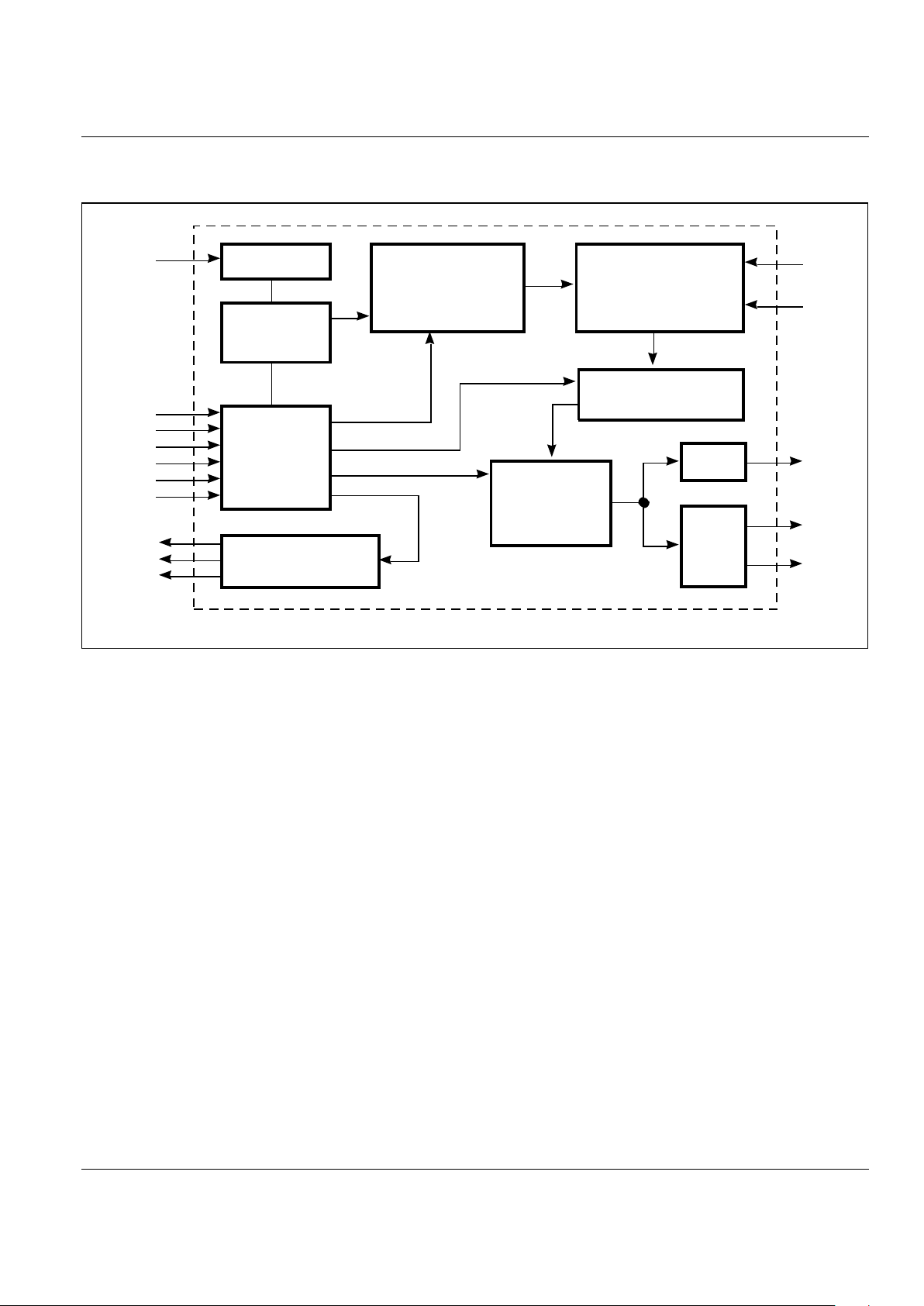
OSCILLATOR
OSC
CLOCK
GENERATOR
CONTROL
LOGIC
TG1
TG2
TG3
TG4
SBT
IRP
OUTPUT
DRIVER
OUT1
OUT2
OUT3
POP NOISE
REDUCTION
ADDRESS
SEQUENCER
VOICE
EPROM
ADPCM
DECODER
BUZZER
BUFFER
D/A
C
OUT
V
OUT1
V
OUT2
GND
V
CC
BLOCK DIAGRAM
APLUS API8108A
Page 4

4
PIN DESCRIPTION
OUT1 Programmable output 1
OUT2 Programmable output 2
OUT3 Programmable output 3
VOUT1 PWM audio signal output for buzzer and speaker
VOUT2 PWM audio signal output for buzzer and speaker
GND Power ground
COUT Current output from internal DAC for speaker playback
OSC Oscillator resistor pin to control sampling frequency
VPP Program power supply, no connect when voice playback
TG1
Trigger switch 1, internal pull low, active high
TG2
Trigger switch 2, internal pull low, active high
VCC Positive power supply
TG3 Trigger switch 3, internal pull low, active high
TG4
Trigger switch 4, internal pull low, active high
SBT Sequential trigger, internal pull low, active high
IRP Interrupt to stop playback, internal pull low, active high
Note:
1. The following pins are used to program data into the memory: pins 4, 5, 6,
8, 9, 12, 15 and 16.
BONDING PARAMETERS
Pin Name X Y
1 OUT1 204 -678
2VOUT1 423 -678
3VOUT2 718 -678
4 GND 893 -678
5 OUT2 786 677
6 OUT3 590 677
7COUT 167 677
8 OSC -89 677
9VPP -306 677
10
TG1
-483 677
11
TG2
-691 677
12 VCC -899 677
13 TG3 -796 -678
14
TG4
-588 -678
15 SBT -380 -678
16 IRP -172 -678
BONDING DIAGRAM
Note: Programming requires connection to
pins 4, 5, 6, 8, 9, 12, 15, and 16.
PIN CONFIGURATIONS
300-mil PDIP
1
2
3
4
5
6
7
8
16
15
14
13
12
11
10
9
OUT1
V
OUT1
V
OUT2
GND
OUT2
OUT3
C
OUT
OSC
IRP
SBT
TG4
TG3
V
CC
TG2
TG1
V
PP
12 11 10 9 8 7 6 5
13 14 15 16 2 413
NC
NC
(0,0)
X
Y
Note: Substrate must be connected to GND
Pad size = 80 mm x 80 mm
Die size = 2128 mm x 16 35
m
m
83.78mil x 64.37 mil
APLUS
API8108A
Page 5

5
ABSOLUTE MAXIMUM RATINGS
Symbol Parameter Value Unit
VCC - GND Terminal Voltage with Respect to GND -0.5 to +7.0 V
VIN GND -0.3 < V IN < VCC + 0.3 V
VOUT GND < VOUT < VCC V
TA Operating Temperature -10 to +85 °C
TSTG Storage Temperature -55 to +125 °C
DC CHARACTERISTICS
Symbol Parameter Description Test Conditions Min. Typ. Max. Unit
VCC Operating Voltage 3.0 4.5 6.0 V
ISB Standby Current Vcc = 3.0V, I/O Open - 1 5 uA
IOP Operating Current Vcc = 3.0V, I/O Open - - 100 uA
VIH Input HIGH Voltage Vcc = 3.0V 2.5 3.0 3.5 V
VIL Input LOW Voltage Vcc = 2.0V - 0.3 0 0.3 V
IOH VOUT HIGH Operating Current Vcc = 3.0V, VOUT = 3.0V - -12 - mA
IOL VOUT LOW Operating Current Vcc = 3.0V, VOUT = 0V - 12 - mA
ICO COUT Operating Current Vcc = 3.0V, VCOUT = 0.7V - - 2 - mA
ISTPH STP HIGH Operating Current Vcc = 3.0V, VSTP = 3.0V - - 5 - mA
ISTPL STP LOW Operating Current Vcc = 3.0V, VSTP = 0V - 5 - mA
ILED LED Output Current Vcc = 2.2V - 6.0V 6 8 10 mA
DF/F Frequency Stability (FOSC [3V] - FOSC [3.5V]) / FOSC (3.0V) - - 5 %
APLUS API8108A
Page 6

6
TIMING WAVEFORMS
1. Level, Unholdable, Non-retriggerable
a. Trigger is shorter than a Group output b. Trigger is longer than a Group output
2. Level Holdable
a. Trigger is shorter than a Group output b. Trigger is longer than a Group output
3. Single Button Trigger (SBT), Sequential
a. Level Unholdable
b. Level Holdable
TG1
Group 2
TG2
C
OUT
LED
STP
Group 1 Group 2 Group 2
TG1
Group 2
TG2
C
OUT
LED
Group 1 Group 2 Group 2
Group 1
SBT
C
OUT
Group 2 Group 2 Group 2 Group N Group 1
Group 1
SBT
C
OUT
Group 2 Group 2 Group 2 Group N Group 1
Where N is up to 8.
APLUS API8108A
Page 7

Group 2
7
a. Trigger is shorter than a phrase output tb. Trigger is longer than a phrase outpu
TG1
Grroup 2
TG2
C
OUT
Group 1 Grouup 2
6. Single Button Trigger (SBT), Sequential
a. Edge Unholdable
5. Edge Holdable
a. Trigger is shorter than a phrase output tb. Trigger is longer than a phrase outpu
TG1
Group2
TG2
C
OUT
LED
Group 1 Group2
APLUS API8108A
4. Edge,Unholdable,Non-retritggerable
STP
LED
b. Edge Holdable
SBT
C
OUT
Group2
Group 1 1Group Group N
SBT
C
OUT
Group 1
1
Group
Group N
Where N is up to 8.
Page 8

APLUS API8108A
tables on page 6.OSC refer to the Sampling Frequency vs. R,OSCTo determine the value of R4.
SP = 8 Ohm speaker.3.
R = 330 Ohm (if using transistor 8050 and Vcc = 4.5V).2.
F).mTo direct dirve a speaker or buzzer, C is needed (C = 0.1 1.
Notes:
OUT3
OUT
C
OSC
R
OSC
IRP
SBT
GND
Vcc
OSC
R
SP
OUT
C
OSC
IRP
R
SBT
GND
Vcc
SPEAKER
32/64 OHM
BUZZER OR
PIEZO
OUT1
V
OSC
R
OUT2
V
C
OSC
R
IRP
SBT
TG4
TG3
TG2
TG1
GND
Vcc
OSC
R
SP
OUT
C
OSC
IRP
SBT
TG4
TG3
TG2
TG1
GND
Vcc
CASCADE APPLICATION
TYPICAL APPLICATION
APPLICATION CIRCUITS
8
Page 9

9
APPLICATION CIRCUITS
PARALLEL APPLICATION
Vcc
GND
TG1
TG2
TG3
TG4
SBT
IRP
OSC
C
OUT
SP
ROSC
Vcc
GND
TG1
TG2
TG3
TG4
SBT
IRP
OSC
C
OUT
ROSC
R
LED APPLICATION
Vcc
GND
TG1
TG2
TG3
TG4
SBT
IRP
OSC
C
OUT
SP
R
OSC
OUT2
OUT1
R
Notes:
The following are typical values:
1. B of NPN transistor > 130.
2. SP = 8W. 1/4W.
3. Piezo buzzer resonant frequency = 1 KHz.
APLUS API8108A
Page 10

10
APPLICATION CIRCUITS
CDS APPLICATION
8-SEGMENT TRIGGER APPLICATION
Vcc
GND
SBT
IRP
OSC
CDS
C
OUT
SP
R
OSC
R
Vcc
GND
TG1
TG2
TG3
TG4
OSC
C
OUT
SW4
SW3
SW7
SW6
SW5
SW8
SW2
SW1
SP
R
OSC
R
APLUS API8108A
 Loading...