

Datasheet APL78L12-KC-TU, APL78L12-KC-TR, APL78L12-DC-TU, APL78L12-DC-TR, APL78L05-KC-TU Datasheet (ANPEC)
...Page 1
APL78L05/12
Three-Terminal Low Current Positive Voltage Regulator
Features General Description
••
•
3-Ternimal Regulators
••
••
•
Maximum Input Voltage : 30V
••
••
•
Output Voltages of 5V,12V
••
••
•
Output Current Up to 100mA
••
••
•
No External Components
••
••
•
Internal Thermal Overload Protection
••
••
• Internal Short-Circuit Limiting
••
••
• Output V oltage Of fered in 4% tolerance
••
••
• SOP-8, SOT-89 and TO-92 Packages.
••
Applications
• Battery-Powered Circuitry
• Post Regulator for Switching Power Supply
This series of fixed-voltage monolithic integrated-circuit voltage regulators is designed for a wide range
of applications. These applications include on-card
regulation for elimination of noise and distribution
problems associated with single-point regulation. In
addition, they can be used with power-pass elements
to make high-current voltage regulators. Each of
these regulators can deliver up to 100mA of output
current. The internal limiting and ternal shutdown features of these regulators make them essentially immune to overload. When used as a replacement for
a Zener diode-resistor combination, an effective improvement in output impedance can be obtained together with lower-bias current.
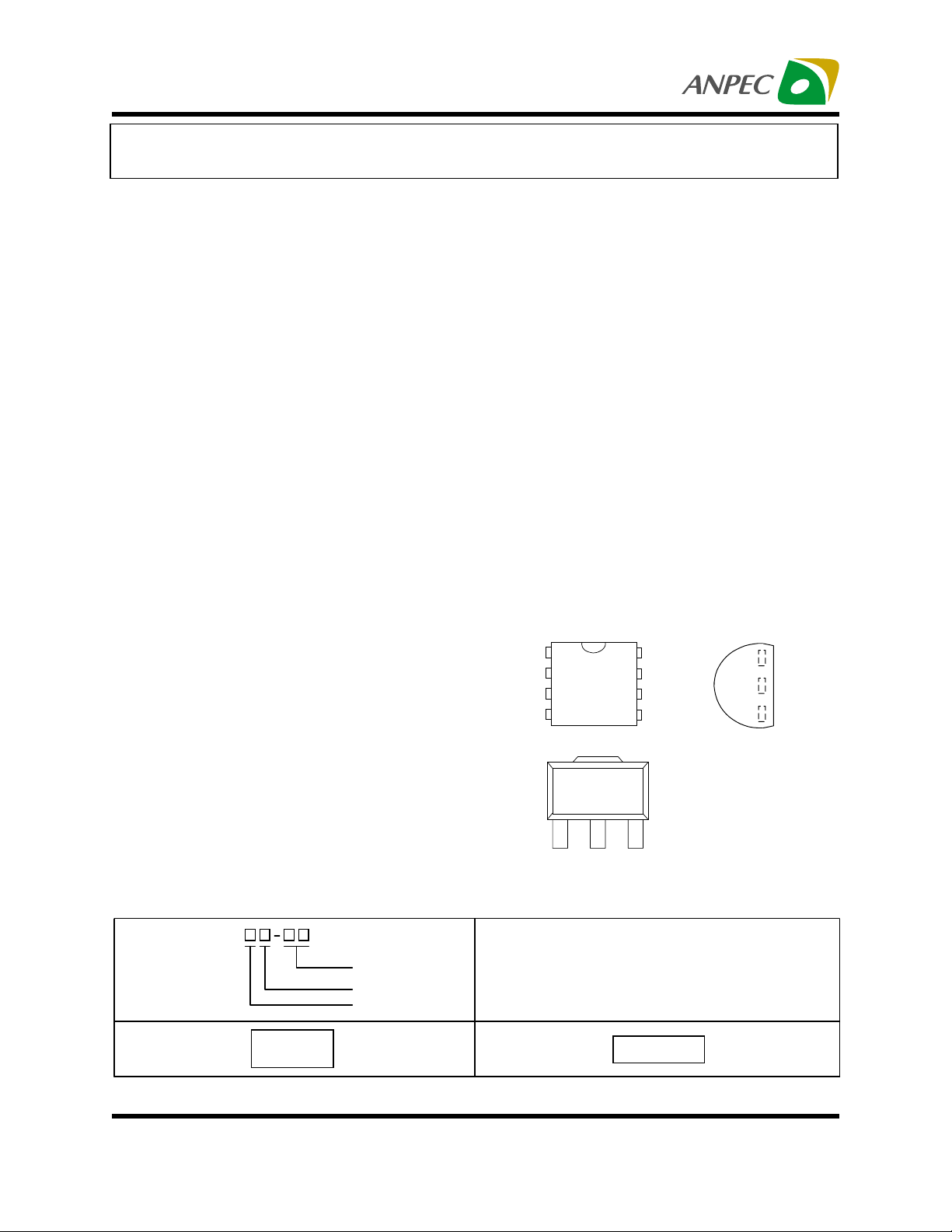
Pin Description
V
GND
GND
NC
1
OUT
2
3
4
8
IN
V
7
GND
6
GND
5
NC
3
IN
V
2
GND
1
OUT
V
SOP-8 (Top View)
213
OUT
GND
V
Ordering and Marking Information
APL 78L05/12 -
Handling Code
Tem p. Range
Package C ode
APL
78L05/12
XXXXX
ANPEC reserves the right to make changes to improve reliability or manufacturability without notice, and advise customers to
obtain the latest version of relevant information to verify before placing orders.
Copyright ANPEC Electronics Corp.
Rev. A.4 - Oct., 2003
XXXXX - Date CodeAP L78L05/12 E :
AP L78L05/12 D/K :
SOT-89 (Front View)
Package C ode
E : T O -9 2 K : S O P - 8 D : S O T -8 9
Tem p. Range
C : 0 to 70 C
Handling Code
TU : Tube TR : Tape & Reel
°
IN
V
AP L78L05/12
XXXXX
TO-92 (Top View)
XXXXX - Date Code
www.anpec.com.tw1
Page 2
APL78L05/12
Absolute Maximum Ratings
Symbol Parameter Rating Unit
VIN Input Voltage 30 VDC
TJ Operating Junction Temperature Range
Control Section
Power Transistor
T
Storage Temperature Range -65 to +150
STG
θ
JA
Thermal Resistance from Junction to Ambient in Free Air
SOP-8
SOT-89/TO-92
Electrical Characteristics
VIN=10V, IOUT=40mA, TJ=25°C, CIN=0.33µF, COUT=0.1µF, unless otherwise specified
Symbol Parameter Test Condition
V
Output Voltage 4.8 5.0 5.2 Vdc
O
≤40mA
OUT
≤20Vdc
IN
≤20Vdc
IN
≤20Vdc
IN
≤100mA
OUT
≤40mA
OUT
≤20Vdc
IN
≤40mA
OUT
OUT
V
Output Voltage (0° to +125°C)
O
Reg
Reg
∆ I
Line Regulation
line
Load Regulation
load
I
Quiesc ent C ur re nt 2.8 6.0 mA
B
Quiescent Current Change
B
VIN-VODropout Voltage I
1.0mA≤I
7.0Vdc≤V
V
=10V, 1.0mA≤I
IN
7.0Vdc≤V
8.0Vdc≤V
1.0mA≤I
1.0mA≤I
8.0Vdc≤V
1.0mA≤I
=100mA 1.9 Vdc
OUT
≤40mA
Min.
4.75 5 5.25 Vdc
0 to 125
0 to 150
160
180
APL78L05
Typ. Max.
29 150
26 100
960
530
0.15 1.5
0.08 0.1
°C
°C
°C/W
Unit
mV
mV
mA
Symbol Parameter Test Condition
V
V
Reg
Reg
∆ I
VIN-VODropout Voltage I
Copyright ANPEC Electronics Corp.
Rev. A.4 - Oct., 2003
Output Voltage 11.5 12 12.5 Vdc
O
1.0mA≤I
Output Voltage (0° to +125°C)
O
Line Regulation
line
Load Regulation
load
I
Quiescent Current 6.5 mA
B
Quiescent C urrent Chan ge
B
14Vdc≤V
V
=19V, 1.0mA≤I
IN
14.5Vdc≤V
1.0mA≤I
1.0mA≤I
16Vdc≤V
1.0mA ≤I
=100mA 1.9 Vdc
OUT
≤40mA
OUT
≤27Vdc
IN
IN
≤100mA
OUT
≤40mA
OUT
≤27Vdc
IN
≤40mA
OUT
OUT
≤27Vdc
≤40mA
Min.
APL78L12
Typ. Max.
Unit
11.4 12 12.6 Vdc
250 mV
100
50
1.5
www.anpec.com.tw2
mV
mA
Page 3
APL78L05/12
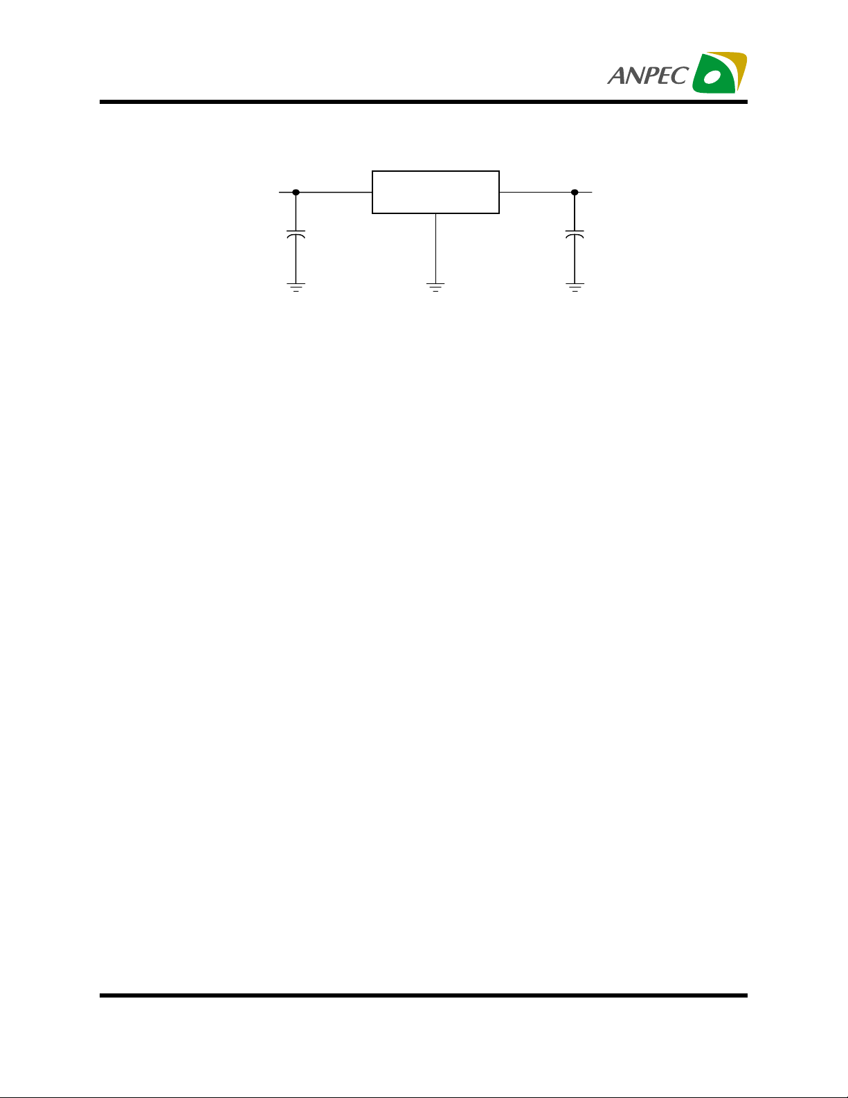
Application Circuit
V
Cin=
0.33
IN
µ
F
APL78L05/12
V
C
0.1
OUT
OUT
=
µ
F
Note1 : A common ground is required between the input and the output voltage. The input voltage must
remain typically 2V above the output voltage even during the low point on the input ripple voltage.
Note2 : Cin is required if regulator is located an appreciable distance from power supply filter.
Note3 : C
is not needed for stability; however, it does improve transient response.
OUT
Copyright ANPEC Electronics Corp.
Rev. A.4 - Oct., 2003
www.anpec.com.tw3
Page 4
APL78L05/12
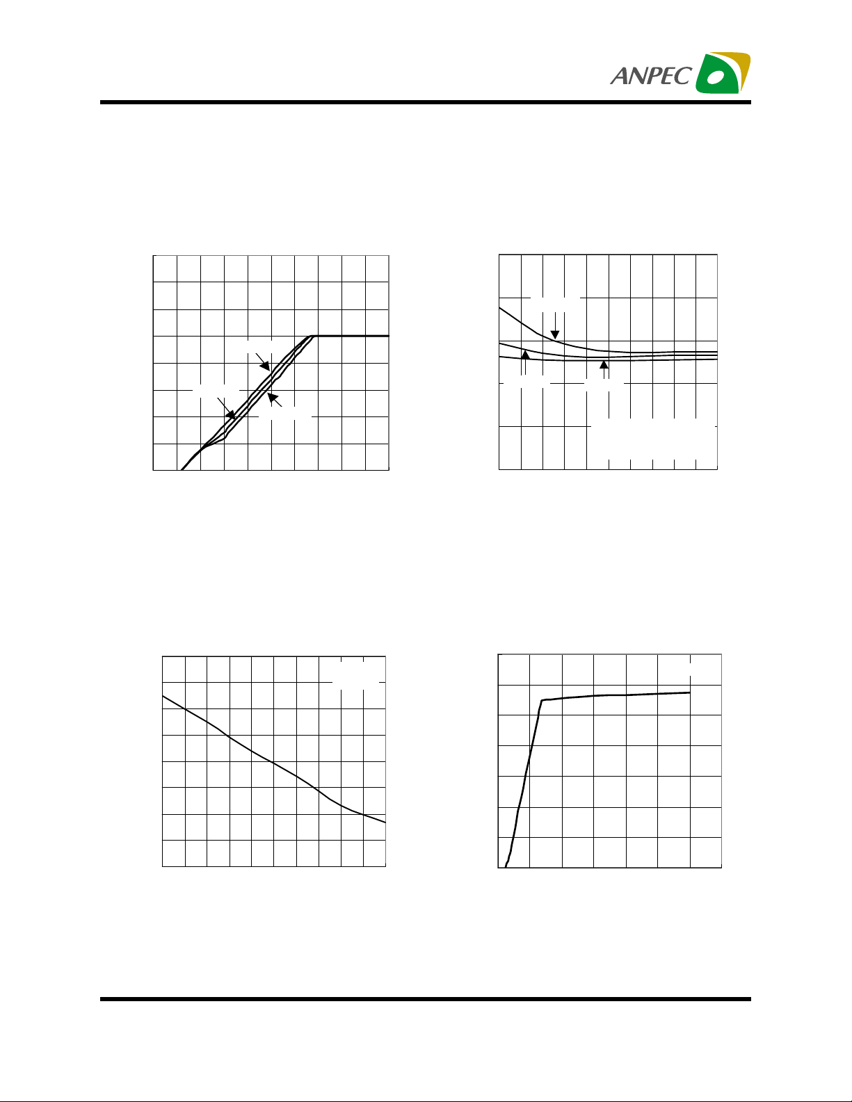
Typical Characteristics
Output Voltage vs. Input Voltage
8
7
6
5
4
3
2
Output Voltage (V)
1
0
0246810
IO=1mA
IO=40mA
IO=100mA
APL78L05
Input Voltage (V)
Quiescent Current vs. Ambient Temperature
3.0
APL78L05
VIN=10V
IO=40mA
Dropout Voltage vs. Junction Temperature
2.25
2
1.75
1.5
Dropout Voltage (V)
1.25
1
IO=70mA
IO=40mA
IO=1mA
Dropout of Regulation is
defined as when
∆∆
∆Vo=1% of Vo
∆∆
0255075100125
APL78L05
Junction Temperature (°C)
Quiescent Current vs. Input Voltage
3.5
3
APL78L05
No Load
2.8
2.6
2.4
Quiescent Current (mA)
2.2
0 25 50 75 100 125
Ambient Temperature (°C)
Copyright ANPEC Electronics Corp.
Rev. A.4 - Oct., 2003
2.5
2
1.5
1
0.5
Quiescent Current (mA)
0
0 5 10 15 20 25 30 35
Input Voltage (V)
www.anpec.com.tw4
Page 5

APL78L05/12
Typical Characteristics (Cont.)
Quiescent Current vs. Output Current
3
2.5
2
1.5
1
0.5
Quiescent Current (mA)
0
0 20406080100
APL78L05 APL78L05
VIN=10V
Output Current (mA)
PSRR vs. Frequency
+0
VIN=10V
IOUT=10mA
-10
APL78L05
Dropout Voltage vs. Output Current
1.9
1.85
1.8
1.75
1.7
Dropout Voltage (V)
1.65
1.6
020406080100
Dropout of
Regulation is
defined as when
∆∆
∆Vo=1% of Vo
∆∆
Output Current (mA)
Load-Transient Response
C
=0.1uF
OUT
COUT=0.1µF
APL78L05
-20
-30
-40
-50
PSRR (dB)
-60
-70
-80
10
100 1k 10k
Frequency (Hz)
Copyright ANPEC Electronics Corp.
Rev. A.4 - Oct., 2003
100k
VOUT(100mv/div)
V
(100mv/div)
OUT
IOUT=
I
=10mA~80mA
OUT
10mA~80mA
Time (20µs/div)
www.anpec.com.tw5
Page 6

APL78L05/12
Typical Characteristics (Cont.)
5.02
5.015
Line Transient Response
VIN=9.5V~10.5V
COUT=0.1µF
OUT=10mA
I
VOUT=10(mV/div)
Time (100us/div)
Output Voltage vs.
Ambient Temperature
VIN=10V
IO=40mA
Maximum Power Dissipation vs.
APL78L05
Ambient Temperature
1300
1100
900
700
500
300
Maximum Power Dissipation (mW)
100
25 50 75 100 125 150
TO-92 Type Package
No Heat Sink
APL78L05
Ambient Temperature (°C)
Region of Stable ESR vs.
APL78L05 APL78L05
10
Output Current
C
OUT
=0.1uF
5.01
5.005
Output Voltage(V)
5
4.995
0 25 50 75 100 125
Ambient Temperature (°C)
Copyright ANPEC Electronics Corp.
Rev. A.4 - Oct., 2003
1
Stable Region
ESR(Ω)
OUT
C
0.1
0.01
020406080100
Untested
Output Current(mA)
www.anpec.com.tw6
Page 7

APL78L05/12
Typical Characteristics
The APL78L05/12 Series of fixed voltage regulators
are designed with Thermal Overload Protection that
shuts down the circuit when subjected to an excessive power overload condition. Internal Short Circuit
Protection limits the maximum current the circuit will
pass.
In many low current applications, compensation capacitors are not required. However, it is recommended that the regulator input be bypassed with a
capacitor if the regulator is connected to the power
supply filter with long wire lengths, or if the output
load capacitance is large. The input bypass capacitor should be selected to provide good high-frequency
characteristics to insure stable operation under all
load conditions. A 0.33µF or larger tantalum, mylar,
or other capacitor having low internal impedance at
high frequencies should be chosen. The bypass capacitor should be mounted with the shortest possible
Figure 1. Current Regulator
Input
0.33µF
APL78L05
R
Constant
Current to
Grounded
l
O
Load
The APL78L00 regulators can also be used as a current source when connected as above. In order to
minimize dissipation the APL78L05 is chosen in this
application. Resistor R determines the current as
follows :
5.0V
IO = + IB
R
IB =3.8mA over line and load changes
For example, a 100mA current source would require
R to be a 50Ω, 1/2W resistor and the output voltage
compliance would be the input voltage less 7V.
Figure 2. ±15V Tracking Voltage Regulator
leads directly across the regulators input terminals.
Good construction techniques should be used to minimize ground loops and lead resistance drops since
the regulator has no external sense lead. Bypassing
the output is also recommended.
Copyright ANPEC Electronics Corp.
Rev. A.4 - Oct., 2003
+20V
0.33µF
0.33µF
20V
APL78L15
MPSU55
6
7
MC1741
4
6.5
2
3
MPSA70
Figure 3. Positive and Negative Regulator
+V
I
0.33µF
-V
I
0.33µF
APL78LXX
0.1µF
APL79LXX
0.1µF
www.anpec.com.tw7
10K
10K
+V
-V
O
+V
O
-V
O
O
Page 8

APL78L05/12
Packaging Information
SOP-8 pin ( Reference JEDEC Registration MS-012)
HE
0.015X45
e1 e2
D
A1
A
1
L
0.004max.
Dim
A 1.35 1.75 0.053 0.069
A1 0.10 0.25 0.004 0. 010
D 4.80 5.00 0.189 0.197
E 3.80 4.00 0.150 0.157
H 5.80 6.20 0.228 0.244
L 0.40 1.27 0.016 0.050
e1 0. 33 0.51 0.013 0.020
e2 1.27BSC 0.50BSC
18
φ
Millimeters Inches
Min. Max. Min. Max.
°
8
°
Copyright ANPEC Electronics Corp.
Rev. A.4 - Oct., 2003
www.anpec.com.tw8
Page 9

APL78L05/12
Package Information
TO-92
3
J
e
e1
L1
Q
A
L2
SEATING PLANE
b2
L
b
2
1
S
E
S
Millimeters Inches
Dim
Min. Max. Min. Max.
A 4.58 5.33 0.170 0.210
φ b
φ b2
φ D
0.41 0.53 0.160 0.021
0.41 0.48 0.160 0.019
4.96 5.20 0.175 0.205
E 3.94 4.19 0.125 0.165
e 2.42 2.66 0.095 0.105
e1 1.15 1.39 0.045 0.055
J 3.43 0.135
L 12.70 0.500
L1 1.27 0.050
L2 6.35 0.250
Q 2.93 0.115
S 2.42 2.66 0.080 0.105
D
Copyright ANPEC Electronics Corp.
Rev. A.4 - Oct., 2003
www.anpec.com.tw9
Page 10

APL78L05/12
Package Information
SOT-89 (Reference EIAJ ED-7500A Reg stration SC-62)
D
D1
H
L
123
a
E
C
Dim
B1
B
e
e1
A
a
Millimeters Inches
Min. Max. Min. Max.
A 1.40 1.60 0.055 0.063
B 0.40 0.56 0.016 0.022
B1 0.35 0.48 0.014 0.019
C 0 .35 0.44 0.014 0 .017
D 4 .40 4.60 0.173 0 .181
D1 1.35 1.83 0.053 0 .072
e 1.50 BSC 0.059 BSC
e1 3.00 BSC 0.118 B SC
E 2.29 2.60 0.090 0.102
H 3 .75 4.25 0.148 0 .167
L 0 .80 1.20 0 .031 0 .047
α
10
°
10
°
Copyright ANPEC Electronics Corp.
Rev. A.4 - Oct., 2003
www.anpec.com.tw10
Page 11

APL78L05/12
Physical Specifications
Terminal Material Solder-Plated Copper (Solder Material : 90/10 or 63/37 SnPb).
Lead Solderability Meets EIA Specification RSI86-91, ANSI/J-STD-002 Category 3.
Reflow Condition (IR/Convection or VPR Reflow)
Reference JEDEC Standard J-STD-020A APRIL 1999
Peak temperature
°
temperature
Pre-heat temperature
183 C
Time
Classificatio n R e flow Profiles
Convection or IR/
Convection
Average ramp-up rate(183°C to Peak) 3°C/second max. 10 °C /second max.
Preheat temperature 125 ± 25°C)
Temperature maintained above 183°C
Time within 5°C of actual peak temperature
Peak temperature range
Ramp-down rate
Time 25°C to peak temperature
120 seconds max.
60 ~ 150 seconds
10 ~ 20 seconds 60 seconds
220 +5/-0°C or 235 +5/-0°C 215~ 219°C or 235 +5/-0°C
6 °C /second max. 10 °C /second max.
6 minutes max.
VPR
Package Reflow Conditions
pkg. thickness ≥≥≥≥ 2.5mm
and all bags
Convection 220 +5/-0 °C Convection 235 +5/-0 °C
VPR 215-219 °C VPR 235 +5/-0 °C
IR/Convection 220 +5/-0 °C IR/Convection 235 +5/-0 °C
pkg. thickness < 2.5mm and
pkg. volume ≥≥≥≥ 350 mm³
pkg. thickness < 2.5mm and p kg .
volume < 350mm³
Copyright ANPEC Electronics Corp.
Rev. A.4 - Oct., 2003
www.anpec.com.tw11
11
Page 12

APL78L05/12
Re lia b ility te s t p ro g r am
Test item Method Description
SOLDERABILITY MIL-STD-883D-2003
HOLT MIL-STD-883D-1005.7
PCT JESD-22-B, A102
TST MIL-STD-883D-1011.9
ESD MIL-STD-883D-3015.7 VHBM > 2KV, VMM > 200V
Latch-U p JESD 78 10ms , Itr > 100mA
Carrier Tape & Reel Dimensions
E
Po
P
P1
245°C , 5 SEC
1000 Hrs Bias @ 125 °C
168 Hrs, 100 % RH , 121°C
-65°C ~ 150°C, 200 C y c les
t
D
Application
SOP-8
F
W
Ao
J
A
A B C J T1 T2 W P E
330±162 ± 1.5
F D D1 Po P1 Ao Bo Ko t
12.75 +
0.1 5
2 + 0.5 12.4 +0.2
D1
C
2± 0.2
T2
B
T1
Bo
12 + 0.3
- 0.1
Ko
8± 0.1 1.75± 0.1
5.5 ± 0.1 1.55±0.1
1.55+ 0.25
4.0 ± 0.1 2.0 ± 0.1 6.4 ± 0.1 5.2± 0.1 2.1± 0.1 0.3±0.013
(mm)
Copyright ANPEC Electronics Corp.
Rev. A.4 - Oct., 2003
www.anpec.com.tw12
Page 13

APL78L05/12
Carrier Tape & Reel Dimensions
Application
TO-92
H2H2
L
L1
T2
T
T1
A D D1 D2 F1,F2 H H1 H2 H2A
3.18~12 4.0±0.2 0.36~0.53 9.0 MAX
H3 H4 L L1 P P1 P2 T T1
27.0 MAX 20.0 MAX 11.0 MAX 2.5 MIN 12.7±0.2 6.35±0.4 50.8±0.5 0.55 MAX 1.42 MAX
T2 W W1 W2
H2H2A
F1F2
P1
P
A
P2
D2
D1
2.5+0.2
-0.1
H3
W2
H4
H
W1
H1
D
16±0.5 9±0.5 0.5 MAX 0.5 MAX
W
0.36~0.68 17.5~19 5.0~7.0 0.5 MAX
(mm)
Cover Tape Dimensions
Application Carrier Width Cov er Tape Width Devices Per Reel
SOP- 8
TO-92
12 9.3 2500
17.5~19 5.0~7.0 2000
Customer Service
Anpec Electronics Corp.
Head Office :
5F, No. 2 Li-Hsin Road, SBIP,
Hsin-Chu, Taiwan, R.O.C.
Tel : 886-3-5642000
Fax : 886-3-5642050
Taipei Branch :
7F, No. 137, Lane 235, Pac Chiao Rd.,
Hsin Tien City, Taipei Hsien, Taiwan, R. O. C.
Tel : 886-2-89191368
Fax : 886-2-89191369
Copyright ANPEC Electronics Corp.
Rev. A.4 - Oct., 2003
www.anpec.com.tw13
 Loading...