

Page 1
APL5331
3A Bus Termination Regulator
Features General Description (Cont.)
••
• Provide Bi-direction Current
••
- Sourcing or Sinking Current up to 3A
••
• 1.25V/0.9V Output for DDR I/II Applications
••
••
• Fast Transient Response
••
••
• High Output Accuracy
••
- ±20mV over Load, VOUT Offset and
Temperature
••
• Adjustable Output Voltage by External Resistors
••
••
• Current-Limit Protection
••
••
• On-Chip Thermal Shutdown
••
••
• Shutdown for Standby or Suspend Mode
••
••
• Simple SOP-8, SOP-8-P with thermal pad,
••
TO-252- 5 and TO-263-5 Packages
Applications
• DDR I/II SDRAM Termination
• SSTL-2/3 Termination Voltage
On-chip thermal shutdown provides protection against
any combination of overload that would create excessive junction temperature. The output voltage of
APL5331 track the voltage at VREF pin. A resistor
divider connected to VIN, GND and VREF pins is
used to provide a half voltage of VIN to VREF pin. In
addition, an external ceramic capacitor and an opendrain transistor connected to VREF pin provides softstart and shutdown control respectively. Pulling and
holding the VREF to GND shuts off the output. The
output of APL5331 will be high impedance after being shut down by VREF or thermal shutdown function.
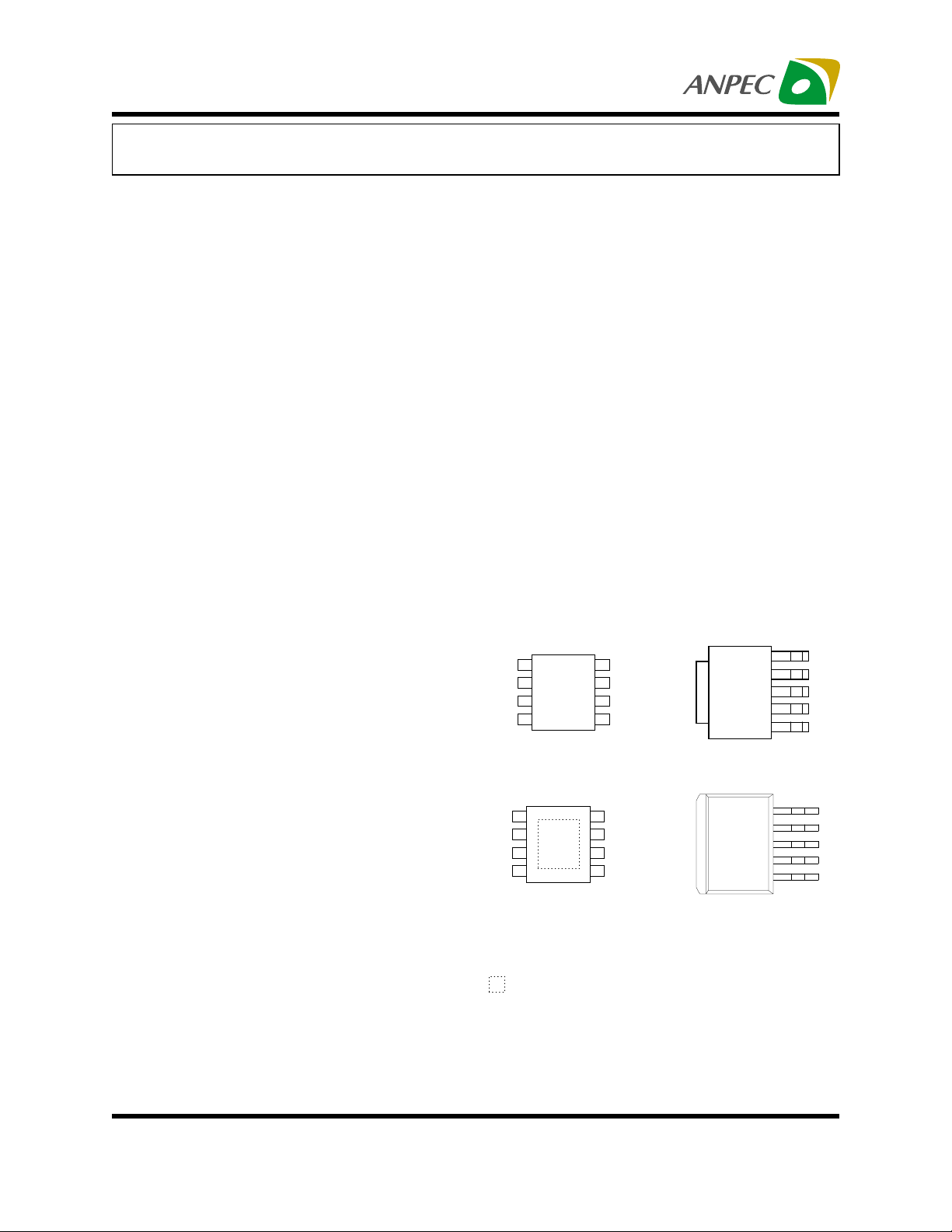
Pin Configuration
12345
VOUT
VREF
VCNTL
GND
VIN
VIN
1
GND
2
VREF
3
VOUT VCNTL
45
VCNTL
8
VCNTL
7
VCNTL
6
TAB is VCNTL
• Applications Requiring the Regulator with
Bi-direction 3A Current Capability
General Description
SOP-8 (Top View)
VIN
1
GND
2
VREF
3
VOUT
45
TO-252-5 (Top View)
NC
8
NC
7
6
VCNTL
NC
TAB is VCNTL
5
4
3
2
1
The APL5331 linear regulator is designed to provide
a regulated voltage with bi-directional output current
SOP-8-P (Top View)
TO-263-5 (Top View)
for DDR-SDRAM termination. The APL5331 integrates
two power transistors to source or sink current up to
3A. It also incorporate current-limit, thermal shutdown and shutdown control functions into a single
NC = No internal connection
= Thermal Pad
(connected to GND plane for better heat
dissipation)
chip. Current-limit circuit limits the short-circuit
current.
ANPEC reserves the right to make changes to improve reliability or manufacturability without notice, and advise
customers to obtain the latest version of relevant information to verify before placing orders.
Copyright ANPEC Electronics Corp.
Rev. A.8 - Oct., 2003
www.anpec.com.tw1
VOUT
VREF
VCNTL
GND
VIN
Page 2
APL5331
Ordering and Marking Information
APL5331
APL5331K C-TR :
APL5331 KAC -TR :
APL5331 U5C -TR :
APL5331 G5C -TR :
Lead Free Code
Handling Code
Tem p. Range
Package Cod e
APL5331
XXXXX
APL5331
XXXXX
Package Cod e
K : SO P-8 KA : SOP-8-P
U5 : TO-252-5 G5 : T O-263-5
Tem p. Range
C : 0 to 7 0
Handling Code
TR : Tape & Re el
Lead Free Code
L : Lead Free Device Blank : Orginal Device
XXXXX - Date Code
XXXXX - Date Code
o
C
Pin Description
PIN NAME I/O DESCRIPTION
Main power input pin. Connect this pin to a voltage source and an input
VIN I
capacitor. The APL5331 sources current to VOUT pin by controlling the upper
NPN pass transistor, providing a current path from VIN pin.
Power and signal ground. Connect this pin to s ystem ground plane with shortest
GND O
traces. The APL5331 sink s current from VOUT pin by controlling the lower NPN
pass transistor, pro viding a current path to GND pin. This pin is also the ground
path fo r inte rn a l co n tr o l c ircu itr y.
Power input pin for internal control circuitry. Connect this pin to a voltage source,
VCNTL I
providing a bias for the internal control circuitry. A bypass capacitor is usually
connected near this pin.
Reference voltage input and active-low shutdown control pin. Apply a voltage to
this pin as a reference voltage for the APL5331. Connect this pin to a resistor
VREF I
divider, between VIN and GND, and a capacitor for soft-start and filtering noise
purposes. Applying and holding this pin low b y an o pen-drain transistor to shut
down th e o u tp u t.
Output pin of the regulator. Connect this pin to load. Output capacitors
VOUT O
connected this pin improves stability and transient response. The output voltage
tracks the reference voltage and is capable of sourcing or sinking current up to
3A.
Block Diagram
VCNTL
VIN
VREF
Copyright ANPEC Electronics Corp.
Rev. A.8 - Oct., 2003
Voltage
Regulation
Shutdown
Therm al
Limit
Current
Limit
VOUT
GND
www.anpec.com.tw2
Page 3
APL5331
Absolute Maximum Ratings
Symbol Parameter Rating Unit
CNTL
V
IN
V
D
P
J
T
STG
T
SDR
T
ESD
V
Thermal Characteristics
VCNTL Supply Voltage, VCNTL to GND -0.2 ~ 7 V
VIN Supply Voltage, VIN to GN D -0.2 ~ 3.9 V
Power Dissipation Internally Limited W
Junction Temperature 150
Storage Temperature -65 ~ 150
Soldering Temperature, 10 Seconds 300
Minimum ESD R ating (Human Body Mode)
±3
o
C
o
C
o
C
kV
Symbol
θ
JA
Thermal Resistance in Free Air
Parameter Rating Unit
SOP-8
SOP-8-P
TO-252-5
TO-263-5
160
80
80
50
°C/W
Recommended Operating Conditions
Symbol Parameter Range Unit
CNTL
V
IN
V
REF
V
OUT
I
J
T
Note1 : The symbol “+” means the VOUT sources current to load; the symbol “-“ means the VOUT sinks
current to GND.
Note2 : The max. IOUT varies with the TJ. Please refer to the typical characteristics.
VCNTL Supply Voltage 3.1 ~ 6V V
VIN Supply Voltage 1.6 ~ 3.5 V
VREF Input Voltage 0.8 ~ 1.75 V
VOUT Output Current (Note1, 2) -3 ~ +3 A
Junction Temperature 0 ~ 125
o
C
Copyright ANPEC Electronics Corp.
Rev. A.8 - Oct., 2003
www.anpec.com.tw3
Page 4
APL5331
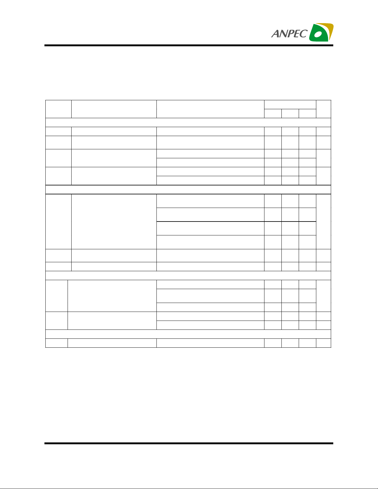
Electrical Characteristics
Refer to the typical application circuit. These specifications apply over, VCNTL=3.3V, VIN=2.5V/1.8V,
VREF=0.5VIN and TJ= 0 to 125°C, unless otherwise specified. Typical values refer to TJ =25°C.
Symbol
Parameter Test Conditions
Output Voltage
VOUT O utput Voltage I
OUT
V
System Accuracy
VOUT O ffset Voltage
OS
V
OUT–VREF
(V
Load Regulation
)
Protection
LIM
Current Limit
I
Thermal Shutdown
SD
T
Tem perature
Therm al Shutdown Hysteres is
Input Current
CNTL
VCNT L Supply Current
I
VREF Bias Current
VREF
I
(The current flows out of VREF)
Shutdown Control
Shutdown Threshold Voltage
APL5331
Min Typ Max
OUT
=0A
Over temperature, VOUT offset, and
load regulation
OUT
I
=+10mA -14
OUT
I
=-10mA
OUT
I
=+10mA to +3A -6
OUT
= -10 mA to -3 A
I
Sourcing Current TJ=25°C
IN
(V
=2.5V) TJ=125°C
Sinking Current TJ=25°C
IN
(V
=2.5V) TJ=125°C
Sourcing Current TJ=25°C
IN
(V
=1.8V) TJ=125°C
J
Sinking Current T
IN
(V
=1.8V) TJ=125°C
Rising T
OUT
I
OUT
I
CNTL
V
REF
V
REF
V
REF
V
J
=0A 2
=±3A (Norm al Operation),
=5V
=GND (S hutdown)
=1.25V/0.9V (Normal Operation)
=GND (Shutdown)
=25°C
-20 20 mV
+3.3 +3.6
-3.3 -3.6
+2.9 +3.2
-2.9 -3.2
0.2
REF
V
-9
2
-3
7
+3.1
-3.1
+2.6
-2.6
150
40
4.5
50 110
2.6
150
20
0.35
Unit
V
mV
8
mV
12
A
o
C
o
C
6
mA
500 nA
40
µA
0.65 V
Copyright ANPEC Electronics Corp.
Rev. A.8 - Oct., 2003
www.anpec.com.tw4
Page 5
APL5331
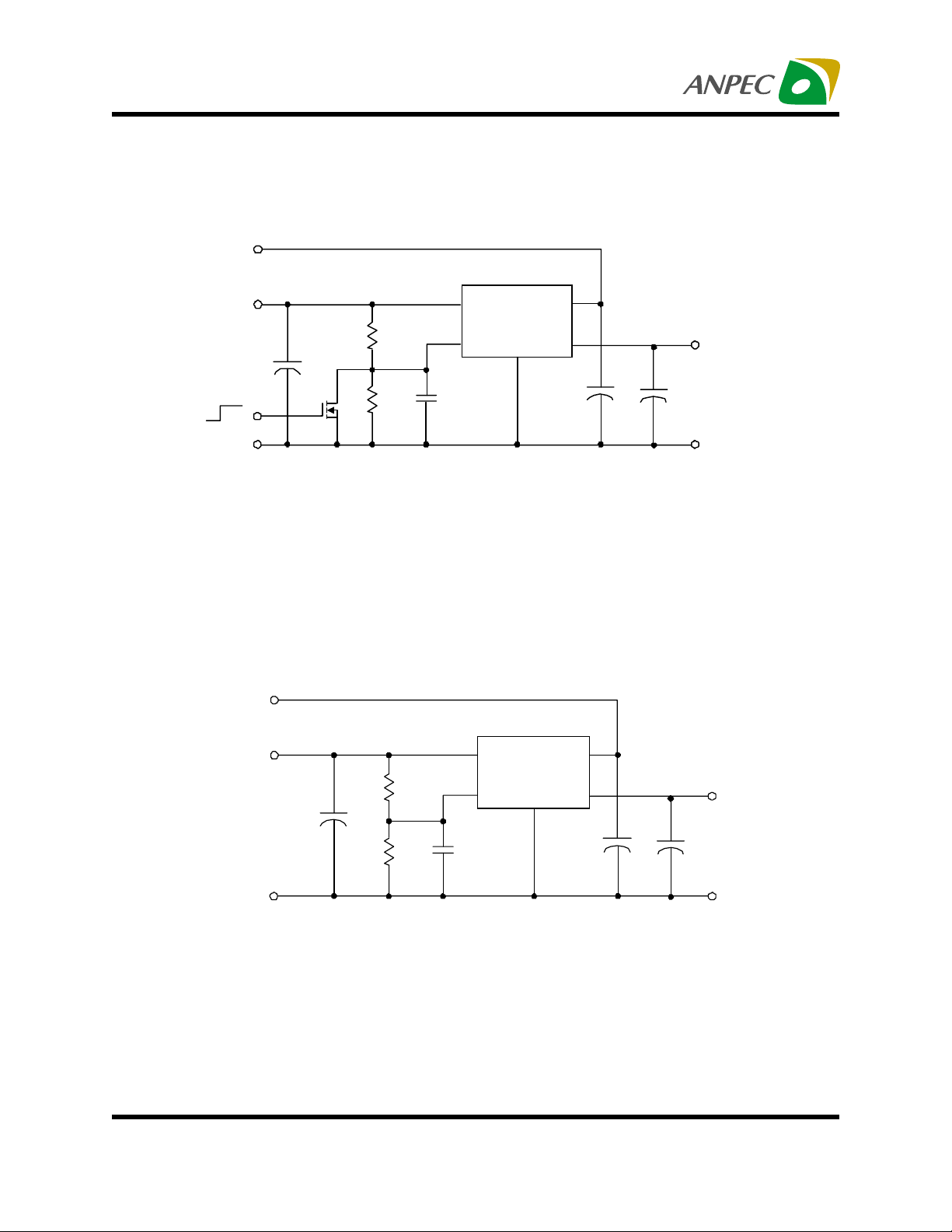
Typical Application Circuit
1. VOUT=1.25V/0.9V Application
V
CNTL
+3.3V
V
IN
+2.5V/1.8 V
R
1
1k
R
2
1k
Q
1
470uF
Shutdown
C
IN
V
REF
C
0.1uF
SS
VIN
VREF
GND
VCNTL
VOU T
C
47uF
CNTL
C
OUT
470uF
V
OUT
+1.25V/0.9V
-3~+3A
GND
COUT : 470µF, ESR=25mΩ
R1, R2 : 1kΩ, 1%
Q1 : APM2300 AC
Note : Since R1 and R2 are very small, the voltage offset
caused by the bias current of VREF can be ignore.
2. VOUT=1.4V Application
CNTL
V
+5V
IN
V
+2.8V
IN
C
470µF
R
1k
R
1k
GND
VIN
1
2
VREF
REF
V
SS
C
0.1µF
GND
VCNTL
VOU T
C
47µF
CNTL
OUT
C
470µF
OUT
V
+1.4V/
-3~+3A
GND
Copyright ANPEC Electronics Corp.
Rev. A.8 - Oct., 2003
GND
www.anpec.com.tw5
Page 6
APL5331
Typical Characteristics
Sourcing Current-Limit
vs Junction T emperature
5.0
4.5
4.0
3.5
3.0
2.5
Current-Limit, ILIM (A)
2.0
VCNTL=5V,VIN=2.5V
VCNTL=3.3V,VIN=2.5V
VCNTL=5V,VIN=1.8V
VCNTL=3.3V,VIN=1.8V
-50 -25 0 25 50 75 100 125
Junction Temperature (°C)
VREF Bias Current
vs Junction T emperature
0.40
V
=1.25V/0.9V
REF
0.35
0.30
0.25
0.20
0.15
0.10
0.05
VREF Bias Current, IVREF (µA)
0.00
-50 -25 0 25 50 75 100 125
Sinking Current-Limit
vs Junction T emperature
-2.0
-2.5
VCNTL=3.3V,VIN=1.8V
-3.0
-3.5
-4.0
Current-Limit, ILIM (A)
-4.5
-5.0
VCNTL=5V,VIN=2.5V
-50 -25 0 25 50 75 100 125
VCNTL=5V,VIN=1.8V
VCNTL=3.3V,VIN=2.5V
Junction Temperature (°C)
VREF Shutdown Threshold
vs Junction T emperature
0.6
0.5
V
=5V
CNTL
0.4
0.3
V
=3.3V
CNTL
0.2
VREF Shutdown Threshold (V)
0.1
-50 -25 0 25 50 75 100 125
Junction Temperature (°C)
Copyright ANPEC Electronics Corp.
Rev. A.8 - Oct., 2003
Junction Temperature (°C)
www.anpec.com.tw6
Page 7
APL5331
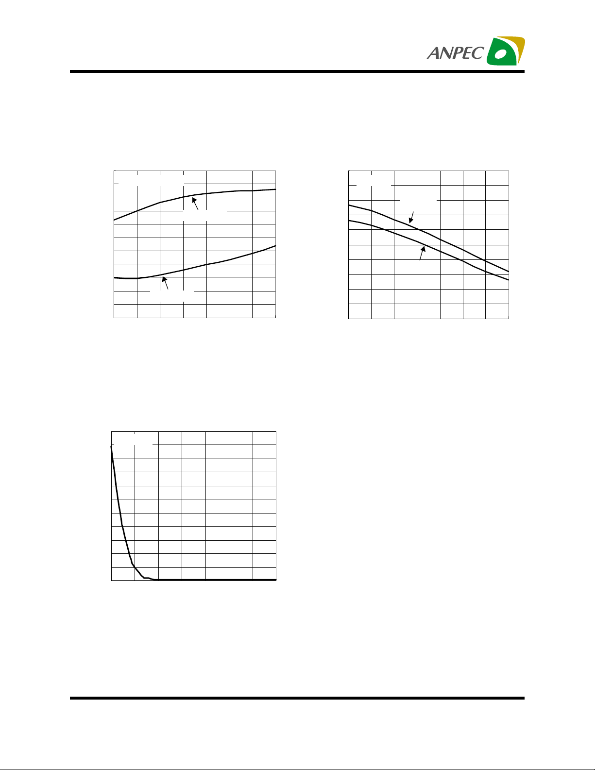
Typical Characteristics (Cont.)
VOUT Offset V oltage
vs Junction T emperature
6
V
=1.25V/0.9V
REF
4
2
0
-2
-4
-6
-8
-10
-12
-14
VOUT Offset V oltage, VOS (mV)
-16
-50 -25 0 25 50 75 100 125
I
OUT
=+10mA
I
OUT
=-10mA
Junction Temperature (°C)
VREF Bias Current
vs VREF Supply Voltage
22
TJ=25°C
20
18
16
14
12
10
8
6
4
VREF Bias Current, IVREF (µA)
2
0
0.0 0.2 0.4 0.6 0.8 1.0 1.2 1.4
Quiescent VCNTL Current
vs Junction T emperature
7.0
I
=0A
6.5
6.0
5.5
5.0
4.5
4.0
3.5
3.0
2.5
Quiescent VCNTL Current (mA)
2.0
OUT
V
=5V
CNTL
V
=3.3V
CNTL
-50-250 255075100125
Junction Temperature (°C)
VREF Supply Votage, VREF (V)
Copyright ANPEC Electronics Corp.
Rev. A.8 - Oct., 2003
www.anpec.com.tw7
Page 8

APL5331
Operating Waveforms
1. Load Transient Response : IOUT = +10mA -> +3A -> +10mA
- VIN = 2.5V, VCNTL = 3.3V
- VREF is 1.250V supplied by a regulator
- COUT = 470µF/10V, ESR = 30mΩ
- IOUT slew rate = ±3A/µS
OUT = +10mA -> +3A
I
IOUT = +10mA -> +3A -> +10mA
Load Regulation = -2.8mV
OUT = +3A -> +10mA
I
V
OUT
I
Ch1 : VOUT, 20mV/Div, DC,
Offset = 1.250V
Ax1 : IOUT, 1A/Div
Time : 1µS/Div
OUT
+10mA
Ch1 : VOUT, 20mV/Div, DC,
Offset = 1.250V
Ax1 : IOUT, 1A/Div
Time : 20µS/Div
+3A
2. Load Transient Response : IOUT = -10mA -> -3A -> -10mA
- VIN = 2.5V, VCNTL = 3.3V
- VREF is 1.250V supplied by a regulator
- COUT = 470µF/10V, ESR = 30mΩ
- IOUT slew rate = ±3A/µS
IOUT = -10mA -> -3A
V
OUT
IOUT = -10mA -> -3A -> -10mA
Load Regulation = +6.2mV
V
OUT
I
OUT
V
OUT
I
OUT
Ch1 : VOUT, 20mV/Div, DC,
Offset = 1.250V
Ax1 : IOUT, 1A/Div
Time : 1µS/Div
IOUT = -3A -> -10mA
V
OUT
V
OUT
I
OUT
Ch1 : VOUT, 20mV/Div, DC,
Offset = 1.250V
Ax1 : IOUT, 1A/Div
Time : 1µS/Div
Copyright ANPEC Electronics Corp.
Rev. A.8 - Oct., 2003
-10mA
Ch1 : VOUT, 20mV/Div, DC,
Offset = 1.250V
Ax1 : IOUT, 1A/Div
Time : 20µS/Div
-3A
I
OUT
I
OUT
Ch1 : VOUT, 20mV/Div, DC,
Offset = 1.250V
Ax1 : IOUT, 1A/Div
Time : 1µS/Div
www.anpec.com.tw8
Page 9

APL5331
Operating Waveforms (Cont.)
3. Load Transient Response : IOUT = +3A -> -3A -> +3A
- VIN = 2.5V, VCNTL = 3.3V
- VREF is 1.250V supplied by a regulator
- COUT = 470µF/10V, ESR = 30mΩ
- IOUT slew rate = ±3A/µS
I
OUT = +3A -> -3A
V
OUT
IOUT = +3A -> -3A -> +3A
OUT = -3A -> +3A
I
V
OUT
V
OUT
Ch1 : VOUT, 50mV/Div, DC,
Offset = 1.250V
Ax1 : IOUT, 2A/Div
Time : 1µS/Div
4. Short-Circuit Test
- V
IN = 2.5V, VCNTL = 3.3V
VOUT is Shorted to GND
I
OUT
-3A
Ch1 : VOUT, 50mV/Div, DC,
Offset = 1.250V
Ax1 : IOUT, 2A/Div
Time : 20µS/Div
I
OUT
+3A
I
OUT
Ch1 : VOUT, 50mV/Div, DC,
Offset = 1.250V
Ax1 : IOUT, 2A/Div
Time : 1µS/Div
VOUT is Shorted to VIN (2.5V)
I
OUT
I
OUT
V
OUT
Ch1 : VOUT, 500mV/Div, DC,
Ax1 : IOUT, 2A/Div
Time : 5mS/Div
Copyright ANPEC Electronics Corp.
Rev. A.8 - Oct., 2003
V
OUT
V
OUT
I
OUT
Ch1 : VOUT, 500mV/Div, DC,
Ax1 : IOUT, 2A/Div
Time : 5mS/Div
www.anpec.com.tw9
Page 10

APL5331
Application Information
General
The APL5331 is a linear regulator and is capable of
sourcing or sinking current up to 3A. The APL5331
has fast transient response, accurate output voltage
(small voltage offset, load regulation), active-low shutdown control and fault protections (current-limit, thermal shutdown). The APL5331 is available in several
packages to meet different of power dissipation in
requirement various applications.
Output V oltage Regulation
The output voltage at VOUT pin tracks the reference
voltage applied at VREF pin. Two internal NPN pass
transistors controlled by separate high bandwidth error amplifiers regulate the output voltage by sourcing
current from VIN pin or sinking current to GND pin.
The base currents of the pass transistors are provided by VCNTL pin. An internal kelvin sensing
scheme use at the VOUT pin for perfect load regulation at various load current. To prevent the two pass
transistors from shoot-through, a small voltage offset
is created between the positive inputs of the two error
amplifiers. This results in higher output voltage while
the regulator sinks light or heavy load current. Since
the APL5331 exhibits very fast load transient
response, lesser amount of capacitors can be use.
In addition, capacitors with high ESR can also be
use.
Current Limit
The APL5331 monitors sourcing and sinking current,
and limits the maximum output current to prevent damages during overload or short-circuit, To increase
the input voltage of VIN or VCNTL will get higher
current-limit points.
Shutdown and Soft-Start
The VREF pin is a dual-function input pin, acting as
reference input and shutdown control input. Applying and holding a voltage below 0.35V(typ.) to VREF
pin shuts down the output of the regulator. An NPN
transistor or N-channel MOSFET is used to pull down
the VREF while applying a “high” signal to turn on the
transistor. When shutdown function is active, the
two pass transistors are turned off and the impedance of the VOUT is about 10MΩ (typ.), sourcing or
sinking no current. When release the VREF pin, the
current through the resistor divider charges the softstart capacitor to initiate a soft-start cycle. The output
voltage tracks the rising VREF. The soft start process
limits the input surge current.
Thermal Shutdown
An thermal shutdown circuit limits the junction temperature of the APL5331. When the junction temperature exceeds TJ= +150oC, a thermal sensor turns
off both pass transistors, allowing the device to cool
down. The regulator starts to regulate again after the
junction temperature reduces by 40oC, resulting in a
pulsed output during continuous thermal overload
conditions. The thermal limit designed with a 40oC
hysteresis lowers the average TJ during continuous
thermal overload conditions, extend life time of
APL5331.
Copyright ANPEC Electronics Corp.
Rev. A.8 - Oct., 2003
www.anpec.com.tw10
Page 11

APL5331
Application Information
Power Inputs
Input power sequence are not required for VIN and
VCNTL. However, do not apply a voltage to VOUT
when there is not voltage VCNTL. This is due to the
internal parasitic diodes between VOUT to VIN and
VOUT to VCNTL which will be forward bias. The
APL5331 can source few current or sinks current up
to 3A for load when the input Voltage at VIN is not
present.
Reference V oltage
A reference voltage is applied at the VREF pin by a
resistor divider between VIN and GND pins. Normally
the bias current of the VREF pin flows out of the IC
and is about 150nA(typ.), creating voltage offset at
the resistor divider and affecting the output voltage
accuracy. The recommended resistor is <5kΩ to
maintain the accuracy of the output voltage. An external bypass capacitor is also connected to VREF.
The capacitor and the resistor divider form a lowpass filter to reduce the inherent reference noise from
VIN. A ceramic capacitor can be use and is selected
to be greater than 0.1µF. Connected the capacitor
as close to VREF as possible for optimal effect. More
capacitance and large resistor divider will increase
the soft-start interval. Do not place any additional loading on this reference input pin.
Output Capacitor
The APL5331 requires a proper output capacitor to
maintain stability over full temperature and current
ranges, and improve transient response. The output
capacitor selection is dependent upon the ESR
(equivalent series resistance) and capacitance of the
output capacitor over full temperature range. The following chart shows the stable region of the output
capacitor for APL5331. The stable region is above
the curve, indicating minimum required ESR and
capacitance to maintain stability. However, the out
put capacitor should have an ESR less than 1Ω.
25
25
ESR (m
ESR (m
20
20
Stable Region
15
15
Ω
Ω
10
10
)
)
5
5
0
0
10 100 1000
10 100 1000
Stable Region
Capacitance(µF)
Capacitance(µF)
Ultra-low-ESR capacitors, such as ceramic chip
capacitors, may promote under-damped transient
response, but proper ceramic chip capacitors placed
near loads can be used as decoupling capacitors. A
low-ESR solid tantalum and aluminum electrolytic capacitor (ESR<1Ω) works extremely well and provides
good transient response and stability over temperature.
The output capacitors are also used to reduce the
slew rate of load current and help the APL5331 to
minimize variations of the output voltage, improving
transient response. For this purpose, the low-ESR
capacitors are recommended and depend on the stepping and slew rate of load current.
Input Capacitor
The input capacitors of VCNTL and VIN pins are not
required for stability but for supplying surge currents
during large load transients, This will prevent the input rail from drooping and improve the performance
of the APL5331. Because of parasitic inductors from
voltage sources or other bulk capacitors to the VCNTL
and VIN pins will limit the slew rate of the surge currents during large load transients, resulting in voltage
drop at VIN and VCNTL pins.
Copyright ANPEC Electronics Corp.
Rev. A.8 - Oct., 2003
www.anpec.com.tw11
Page 12

APL5331
A capacitor of 1µF (ceramic chip capacitor) or greater
(aluminum electrolytic capacitor) is recommended to
connect near VCNTL pin. For VIN pin, an aluminum
electrolytic capacitor (>50µF) is recommended. It is
not necessary to use low-ESR capacitors.
Layout and Thermal Consideration
The input capacitors for VIN and VCNTL pins are
normally placed near each pin for good
performances. Ceramic decoupling capacitors at
output must be placed as close to the load to reduce
the parasitic inductors of traces. It is also recommended that the APL5331 and output capacitors are
placed near the load for good load regulation and
load transient response. The negative pins of the input and output capacitors and the GND pin of the
APL5331 should connect to analog ground plane of
the load.
See figure 1. The SOP-8-P utilizes a bottom thermal
pad to minimize the thermal resistance of the package,
making the package suitable for high current
applications. The thermal pad is soldered to the top
ground pad and is connected to the internal or bottom ground plane by several vias. The printed circuit
board (PCB) forms a heat sink and dissipates most
of the heat into ambient air. The vias are recommended to have proper size to retain solder, helping
heat conduction.
Thermal resistance consists of two main elements,
? JC (junction-to-case thermal resistance) and ? CA
(case-to-ambient thermal resistance). ? JC is specified from the IC junction to the bottom of the thermal
pad directly below the die. ?CA is the resistance from
the bottom of thermal pad to the ambient air and it
includes ? CS (case-to-sink thermal resistance) and
?SA (sink-to-ambient thermal resistance). The speci-
fied path for heat flow is the lowest resistance path
and it dissipates majority of the heat to the ambient
air. Typically , ?CA is the dominant thermal resistance.
Therefore, enlarging the internal or bottom ground
plane reduces the resistance ?CA . The relationship
between power dissipation and temperatures is the
following equation :
PD = (TJ - TA) / ?JA
where,
PD : Power dissipation
TJ : Junction Temperature
TA : Ambient Temperature
? JA : Junction-to-Ambient Thermal Resis tance
102 mil
118 mil
Ambient
Air
SOP-8-P
Die
Vias
Thermal
pad
Internal
ground
plane
Top
ground
pad
Printed
circuit
board
Figure 1 Package Top and side view
Figure 2 shows a board layout using the SOP-8-P
package. The demo board is made of FR-4 material
and is a two-layer PCB. The size and thickness are
65mm* 65mm and 1.6mm. An area of 140mil*105mil
on the top layer is use as a thermal pad for the
APL5331 and this is connected to the bottom layer
by vias. The bottom layer using 2 oz. copper acts as
the ground plane for the system. The PCB and all
components on the board form a heat sink. The ?JA
of the APL5331(SOP-8-P) mounted on this demo
board is about 37oC/W in free air. Assuming the
TA=25oC and the maximum TJ=150oC (typical thermal
limit temperature), the maximum power dissipation is
calculated as :
Copyright ANPEC Electronics Corp.
Rev. A.8 - Oct., 2003
www.anpec.com.tw12
Page 13

APL5331
PD (max) = (150 - 25) / 37
= 3.38W
If the TJ is designed to be below 125oC, the calculated power dissipation should be less than :
PD = (125 - 25) / 37
= 2.70W
APL5331
Figure 2(c) Bottom layer
Figure 2(a) TopOver layer
APL5331
Figure 2(b) Top layer
Copyright ANPEC Electronics Corp.
Rev. A.8 - Oct., 2003
www.anpec.com.tw13
Page 14

APL5331
Packaging Information
SOP-8 pin ( Reference JEDEC Registration MS-012)
HE
0.015X45
e1 e2
D
A1
A
1
L
0.004max.
Dim
A 1.35 1.75 0.053 0.069
A1 0.10 0.25 0.004 0.010
D 4.80 5.00 0.189 0.197
E 3.80 4.00 0.150 0.157
H 5.80 6.20 0.228 0.244
L 0.40 1.27 0.016 0.050
e1 0.33 0.51 0.013 0. 020
e2 1.27BSC 0.50BSC
18
φ
Millimeters Inches
Min. Max. Min. Max.
°
8
°
Copyright ANPEC Electronics Corp.
Rev. A.8 - Oct., 2003
www.anpec.com.tw14
Page 15

APL5331
Packaging Information
SOP-8-P pin ( Reference JEDEC Registration MS-012)
E1
HE
0.015X45
D1
e1 e2
D
A1
A
1
L
0.004max.
Dim
A 1.3 5 1.75 0.053 0.069
A1 0.10 0.25 0.004 0.0 10
D 4.80 5.00 0.189 0.197
D1
E 3.8 0 4.00 0.150 0.157
E1 2.60REF 0.102REF
H 5.80 6.20 0.228 0.244
L 0.40 1.27 0.016 0.050
e1 0.33 0.5 1 0.013 0.020
e2 1.27BSC 0.50BSC
φ 18° 8°
Millimeters Inches
Min. Max. Min. Max.
3.00REF
0.11 8REF
Copyright ANPEC Electronics Corp.
Rev. A.8 - Oct., 2003
www.anpec.com.tw15
Page 16

APL5331
Packaging Information
TO-252-5
A
B
CD
M
PS
K
H
J
L
E1
D1
Dim
Min. Max. Min. Max.
A 6.40 6.80 0.25 0.26
B 5.20 5.50 0.20 0.21
C 6.80 7.20 0.26 0.27
D 2.20 2.80 0.08 0.11
D1 5.2REF 0.205REF
E1 5.3REF 0.209REF
P 1.27REF 0.05REF
S 0.50 0.80 0.02 0.03
H 2.20 2.40 0.08 0.09
J 0.45 0.55 0.01 0.02
K 0.45 0.60 0.018 0.024
L 0.90 1.50 0.03 0.06
M 5.40 5.80 0.21 0.22
Copyright ANPEC Electronics Corp.
Rev. A.8 - Oct., 2003
Millimeters Inches
www.anpec.com.tw16
Page 17

APL5331
Packaging Information
TO-263-5
D
BE
L
b
L1
e
e1
L2
A
c1
v
A1
c
Dim
A
b
b1
c
c1
D
E
L
L1
Min. Max. Min. Max.
4.06 4.83
0.50 0.99
1.52 1.83
0.457 0.736
1.14 1.40
8.25 9.66
9.65 10. 29
14.60 15.88
2.28 2.80
L2
Copyright ANPEC Electronics Corp.
Rev. A.8 - Oct., 2003
Millimeter s Inches
0.160 0.190
0.020 0.039
0.060 0.072
0.018 0.029
0.045 0.055
0.325 0.380
0.380 0.405
0.575 0.625
0.090 0.110
1.40
0.055
www.anpec.com.tw17
Page 18

APL5331
Physical Specifications
Terminal Material Solder-Plated Copper (So lder Material : 90/10 or 63/37 SnPb)
Lead Solderab ility Meets EIA Specification RSI86-91, A NSI/J-STD-002 Category 3.
Reflow Condition (IR/Convection or VPR Reflow)
Reference JEDEC Standard J-STD-020A APRIL 1999
Peak temperature
temperature
Pre-heat temperature
°
183 C
Time
Classification Reflow Prof iles
Convection or IR/
Convection
Average ramp-up rate(183°C to Peak) 3°C/second max. 10 °C /second max .
Preheat temperature 125 ± 25°C)
Temperature maintained above 183°C
Time within 5°C of actual peak temperature
Peak temperature range
Ramp-down rate
Time 25°C to peak temperature
120 seconds max
60 – 150 seconds
10 –20 seconds 60 seconds
220 +5/-0°C or 235 +5/-0°C 215-219°C or 235 +5/-0°C
6 °C /second max . 10 °C /second max .
6 minutes max.
VPR
Package Reflow Conditions
pkg. thickness
and all bgas
Convection 220 +5/-0 °C Convection 235 +5/-0 °C
VPR 215-219 °C VPR 235 +5/-0 °C
IR/Convection 220 +5/-0 °C IR/Convection 235 +5/-0 °C
Copyright ANPEC Electronics Corp.
Rev. A.8 - Oct., 2003
2.5mm
≥≥≥≥
pkg. thickness < 2.5mm and
pkg. volume
350 mm³
≥≥≥≥
pkg. thickness < 2.5mm and pkg.
volume < 350mm³
www.anpec.com.tw18
Page 19

APL5331
R e lia bility te s t pro g r a m
SOLDERA BILITY MIL-STD-883D-2003
HO LT MIL-STD-883D-1005.7
PCT JESD-22-B, A102
TST MIL-STD-883D-1011.9
245°C , 5 SEC
1000 Hrs Bias @ 125 °C
168 Hrs, 100 % RH , 121°C
-65°C ~ 150°C, 200 Cycles
ESD MIL-STD-883D -3015.7 VHBM > 2KV, VMM > 200V
La tc h -Up J E SD 7 8 10 ms , Itr > 100mA
Carrier Tape
t
Test item Method D escription
E
F
W
Po
P
P1
Ao
D
Bo
Ko
D1
T2
A
Copyright ANPEC Electronics Corp.
Rev. A.8 - Oct., 2003
J
C
B
T1
www.anpec.com.tw19
Page 20

APL5331
Application
SOP- 8
SOP-8-P
Application
TO-252
Application
TO-263
A B C J T1 T2 W P E
330 ± 1 62 +1.5
F D D1 Po P1 Ao Bo Ko t
5.5± 1 1.55 +0.1 1.55+ 0.25 4.0 ± 0.1 2.0 ± 0.1 6.4 ± 0.1 5.2± 0. 1 2.1± 0.1 0.3±0.013
A B C J T1 T2 W P E
330 ±3100 ± 213 ± 0. 5 2 ± 0.5
F D D1 Po P1 Ao Bo Ko t
7.5 ± 0.1 1.5 +0.1 1.5± 0.25 4.0 ± 0.1 2.0 ± 0.1 6.8 ± 0.1 10.4± 0.1 2.5± 0.1 0.3±0.05
A B C J T1 T2 W P E
380±380 ± 213 ± 0. 5 2 ± 0.5 24 ± 42± 0.3
F D D1 Po P1 Ao Bo Ko t
11.5 ± 0.1 1.5 +0.1 1.5± 0.25 4.0 ± 0.1 2.0 ± 0.1 10.8 ± 0.1 16.1± 0.1 5.2± 0.1 0.35±0.013
12.75+
0.15
Cover Tape Dimensions
Application Carrier Width Cover Tape Width Devices Per Reel
SOP- 8 / SOP -8-P
TO- 252
TO- 263
12 9.3 2500
16 13.3 2500
24 21.3 1000
2 ± 0.5 12.4 ± 0.2 2 ± 0.2 12± 0. 3 8± 0.1 1.75±0.1
16.4 + 0.3
-0.2
2.5± 0.5
16+ 0.3
- 0.1
24 + 0.3
- 0.1
8 ± 0.1 1.75± 0.1
16 ± 0.1 1.75± 0.1
Customer Service
Anpec Electronics Corp.
Head Office :
5F, No. 2 Li-Hsin Road, SBIP,
Hsin-Chu, T aiwan, R.O.C.
T el : 886-3-5642000
Fax : 886-3-5642050
Taipei Branch :
7F, No. 137, Lane 235, Pac Chiao Rd.,
Hsin Tien City, T aipei Hsien, Taiwan, R. O. C.
T el : 886-2-89191368
Fax : 886-2-89191369
Copyright ANPEC Electronics Corp.
Rev. A.8 - Oct., 2003
www.anpec.com.tw20
Page 21

 Loading...