

Page 1
APL1117
1A Low Dropout Fast Response Positive Adjustable Regulator and Fixed
1.8V, 2.5V, 2.85V and 3.3V
Features
••
•
Guaranteed Output Voltage Accuracy within 2%
••
••
•
Fast Transient Response
••
••
•
Guaranteed Dropout Voltage at Multiple
••
Currents
••
•
Load Regulation : 0.1% Typ.
••
••
•
Line Regulation : 0.03% Typ.
••
••
• Low Dropout Voltage : 1.1V Typ. at I
••
••
• Current Limit : 1A Typ. at T
••
••
• On-Chip Thermal Limiting : 150°C Typ.
••
••
• Adjustable Output : 1.25~10.7V
••
••
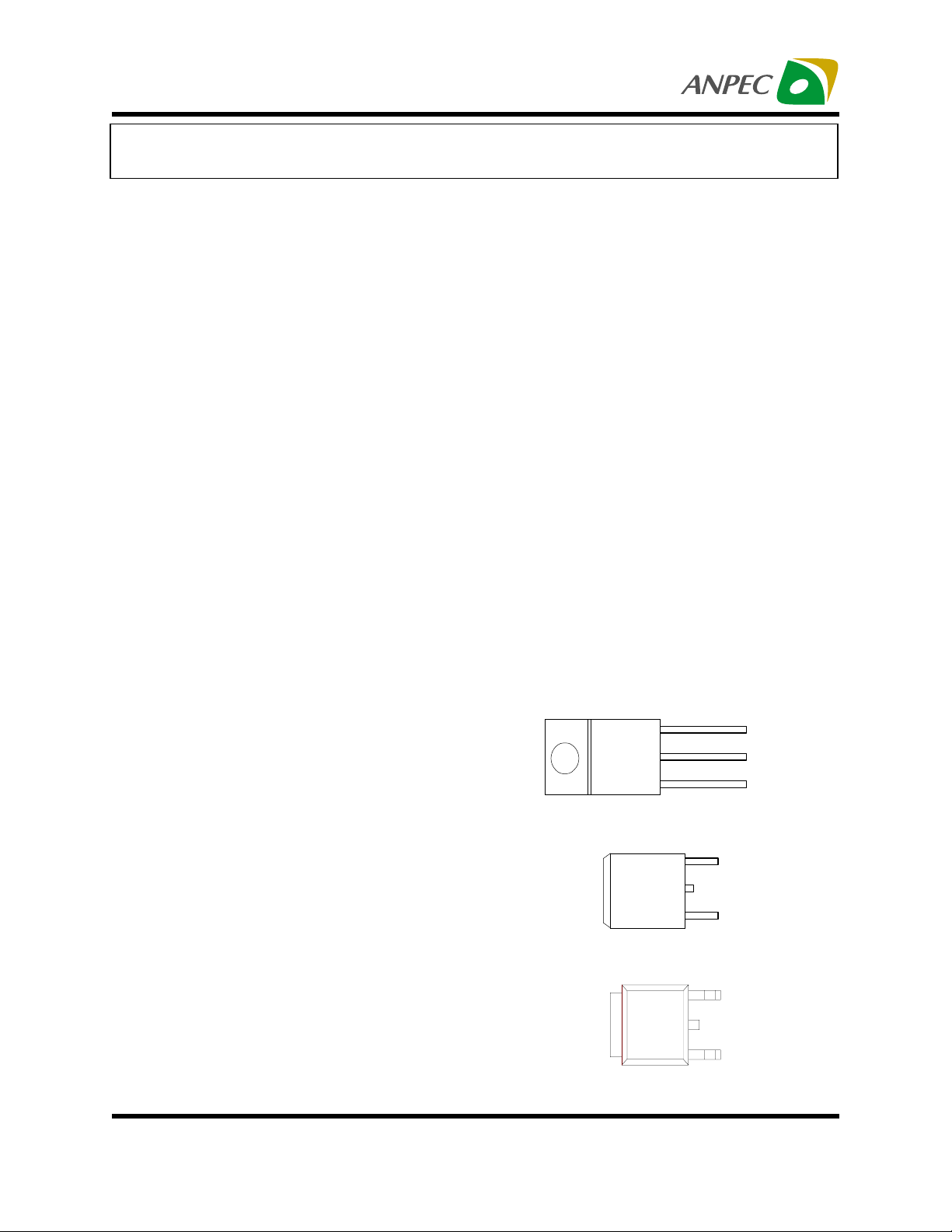
• Standard 3-pin TO-220, TO-252, TO-263 and
••
SOT-223 Power Packages
=25°C
J
OUT
=1A
Applications
General Description
The APL1117 is a low dropout three-terminal adjustable regulators with 1A output current capability. In
order to obtain lower dropout voltage and faster transient response, which is critical for low voltage applications , the APL1117 has been optimized. The
device is available in an adjustable version and fixed
output voltages of 1.8V, 2.5V, 2.85V and 3.3V. The
output available voltage range of an adjustable version is from 1.25~10.7V with an input supply below
12V. Dropout voltage is guaranteed at a maximum of
1.3V at 1A. Current limit is trimmed to ensure specified output current and controlled short-circuit current.
On-chip thermal limiting provides protection against
any combination of overload that would create excessive junction temperatures. The APL1117 is available
in the industry standard 3-pin TO-220, TO-252, TO263, and the low profile surface mount SOT-223
power packages which can be used in applications
where space is limited.
Pin Description
••
• Active SCSI Terminators
••
••
• Low Voltage Logic Supplies
••
••
• Battery-Powered Circuitry
••
••
• Post Regulator for Switching Power Supply
••
TAB is V
TAB IS V
ANPEC reserves the right to make changes to improve reliability or manufacturability without notice, and advise
customers to obtain the latest version of relevant information to verify before placing orders.
Copyright ANPEC Electronics Corp.
Rev. B.8 - Jun., 2003
1
Front View for TO-220
3
2
1
Front View for TO-263
3
OUT
Front View for TO-252
OUT
2
1
3
2
1
V
IN
V
OUT
ADJ/GND
V
IN
V
OUT
ADJ/GND
V
IN
V
OUT
ADJ/GND
www.anpec.com.tw
Page 2
APL1117
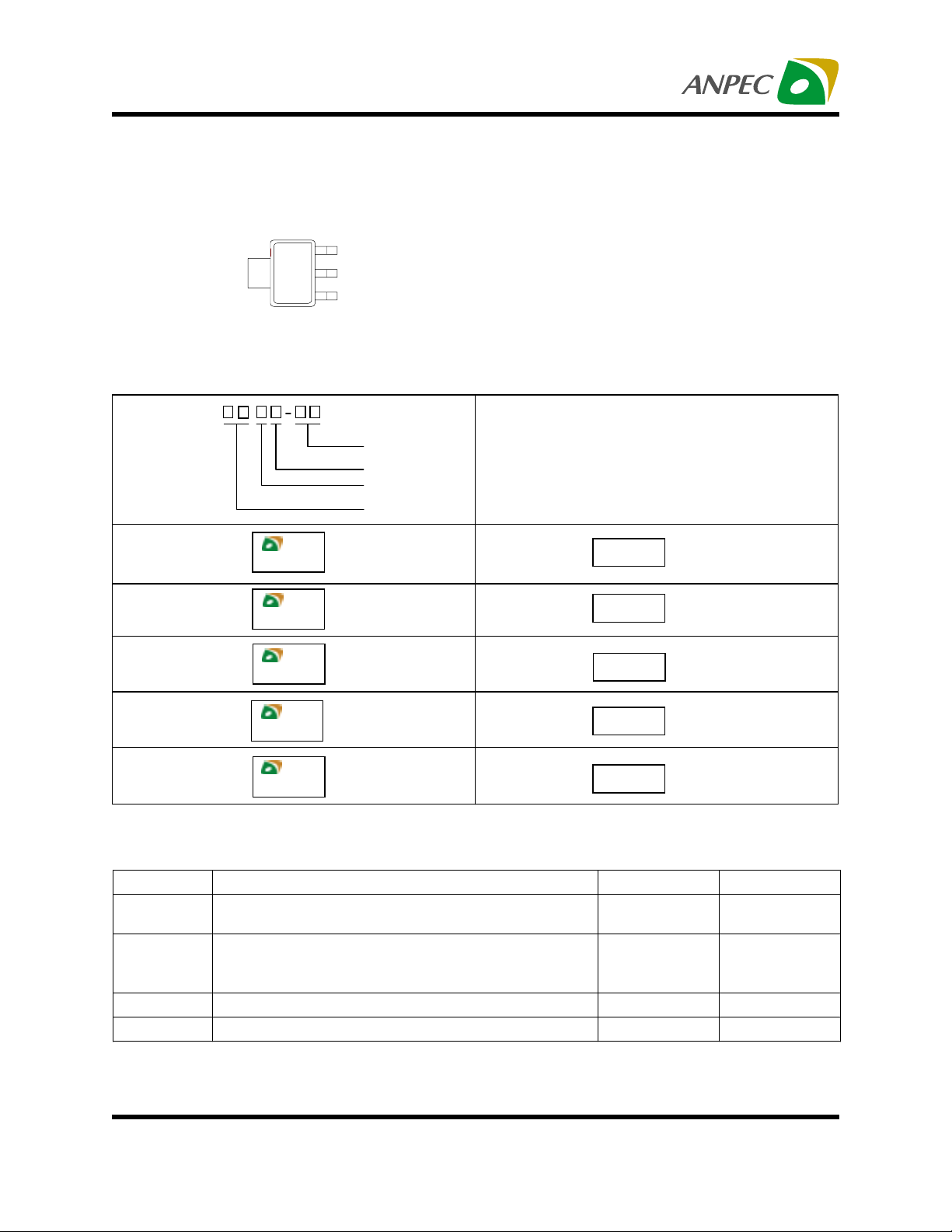
Pin Description (Cont.)
Front View for SOT-223
3
IN
T A B IS V
Ordering and Marking Information
OUT
OUT
2
1
ADJ/GN D
APL1117-
Handling Code
Tem p. Range
Package Code
Voltage Code
APL1117 F /G/U :
APL1117-18F/G/U :
APL1117-25F/G/U :
APL1117-28F/G/U :
APL1117
XXXXX
APL1117
XXXXX
25
APL1117
XXXXX
28
APL1117
XXXXX
33
APL1117
XXXXX
18
XXXXX
XXXXX
XXXXX
- D a te C od e
- D a te C od e
- D a te C od eXXXXX
- Date CodeXXXXX
- D a te C od e
Absolute Maximum Ratings
Package Code
F : T O -22 0 G : T O-26 3 U : T O -2 52 V : S OT-2 2 3
Tem p. Range
C : 0 to 70 C
Handling Code
TU : T u be TR : T ap e & R ee l
Voltage Code
18 : 1.8 V 25 : 2 .5V 28 : 2.8 5V 33 : 3.3 V
Blank : Adjustable Version
APL1117 V :
APL1117-28V :
°
APL1117
XXXXX
APL1117
XXXXX18
APL1117
XXXXX25
APL1117
XXXXX28
APL1117
XXXXX33
XXXXX - Date Code
XXXXX - Date CodeAPL1117-18V :
XXXXX - Date CodeAPL1117-25V :
XXXXX - Date Code
XXXXX - Date CodeAPL1117-33V :APL1117 -33F/G/U :
Symbol Parameter Rating
V
I
Input Voltage APL1117, APL1117-33
APL1117-18, APL1117-25, APL1117-28
T
J
Operating Junction Temperature Range
Control Section
Power Transistor
T
STG
T
L
Storage Temperature Range -65 to +150
Lead Temperature (Soldering, 10 second) 260
(Note)
15
9
0 to 125
0 to 150
Note : The values here show the absolute maximum rating, and for normal usage please refer the test condition in Electrical
Characteristics Table.
Copyright ANPEC Electronics Corp.
2
www.anpec.com.tw
Rev. B.8 - Jun., 2003
Unit
V
C
°
C
°
C
°
Page 3
APL1117
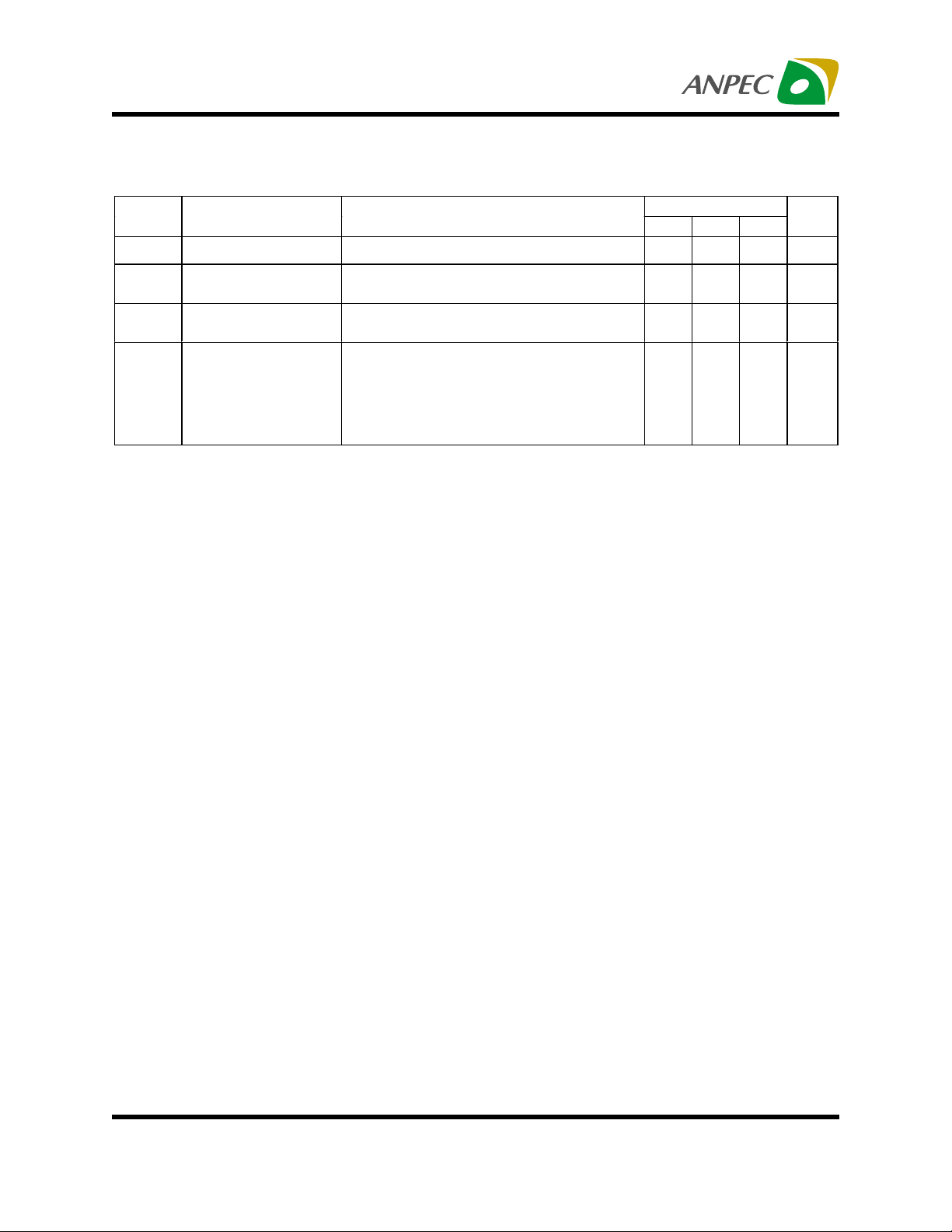
Electrical Characteristics (Cont.)
V
V
Reference Voltage
REF
Output Voltage
OUT
APL1117-18
APL1117-25
APL1117-28
APL1117-33
REG
Line Regulation
LINE
APL1117
APL1117-18
APL1117-25
APL1117-28
APL1117-33
REG
Load Regulation
LOAD
APL1117
APL1117-18
APL1117-25
APL1117-28
APL1117-33
Dropout Voltage
D
I
LIMIT
I
Current Limit
Adjust Pin Current
ADJ
APL1117
Adjust Pin Current
I
∆
ADJ
Change APL1117
I
Minimum Load
O
Current APL1117
PSRR Ripple R eje ctio n f
T
T
Thermal Regulation
R
Temperature
S
Stability
L
S
Long -Term
Stability
10mA≤ I
T
=0~125°C
J
T
=0~125°C,
J
0≤ I
OUT
=0~125°C,
T
J
0≤ I
OUT
=0~125°C,
T
J
0≤ I
OUT
=0~125°C,
T
J
0≤ I
OUT
I
10mA, 1.5V≤(V
=
OUT
I
0A, 3.5V≤V
=
OUT
I
0A, 4V≤V
=
OUT
I
0A, 4.25V≤V
=
OUT
I
0A, 4.75V≤V
=
OUT
(V
IN -VOUT
VIN=3.5V, 0≤ I
V
=4V, 0≤ I
IN
VIN=4.25V, 0≤ I
VIN=4.75V, 0≤ I
I
=100mA
OUT
=500mA
I
OUT
I
=1A
OUT
(V
IN -VOUT
(V
IN -VOUT
10mA≤ I
1.4V≤(V
(V
IN -VOUT
=120Hz, V
RIPPLE
(V
IN -VOUT
T
=25°C, 30ms Pulse
J
=125°C,1000Hrs.
T
J
1A, 1.4V≤(V
≤
OUT
1.5A, 3.5V≤V
≤
1A, 4V≤V
≤
1A, 4.25V≤V
≤
1A, 4.75V≤V
≤
IN
≤
IN
=3V, 0≤ I
)
OUT
≤
OUT
OUT
OUT
(Note2)
(Note2)
(Note2)
)=5V, TJ=25°C
=3V, I
)
OUT
1A,
≤
OUT
≤10.75V
)
IN -VOUT
)=10.75V
=3V
)
APL1117Symbol Parameter Test Conditions
Min. Typ. Max.
≤10.75V,
)
≤
IN
IN -VOUT
9V
≤
5.5V
5.15V
≤
IN
7.75V
≤
IN
OUT
1A
≤
(Note1)
1A
1A
≤
1A
≤
IN
9V,
≤
IN
IN
(Note1)
(Note1)
≤
(Note1)
≤
9V,
≤
1A
(Note1)
(Note1)
IN -VOUT
9V,
12V,
)≤10.75V
(Note1)
(Note1)
(Note1)
1.225 1.250 1.275
1.764 1.800 1.836
2.450 2.500 2.550
2.790 2.850 2.910
3.235 3.300 3.365
(Note1)
0.03
1
1
1
1
0.1
1
1
1
1
11.1V
1.05
1.1
1000 mA
=10mA 60 120
0.2 5
(Note3)
RIPPLE
=1V
P-P,
1.7 mA
60 75 dB
0.01 0.02 %/ W
0.5 %
0.3 %
0.2
6
6
6
6
0.4
10
10
10
10
1.2
1.3
Unit
V
V
%
mV
%
mV
V
A
µ
A
µ
Copyright ANPEC Electronics Corp.
Rev. B.8 - Jun., 2003
3
www.anpec.com.tw
Page 4
APL1117
Electrical Characteristics (Cont.)
Symbol Parameter Test Conditions
V
RMS Output Noise
N
Thermal Resistance Junction to C ase, at Tab
θ
th
T
=25°C,10Hz≤F≤10kHz, (% of V
J
Junction to Ambient
OT
Over Temperature
OUT
)
APL1117
Min. Typ. Max.
0.003 %
15
50
150
Unit
C/ W
°
°
C
Point
I
Quiescent Current
Q
APL1117-18
APL1117-25
APL1117-28
APL1117-33
Note 1 : See thermal regulation specifications for changes in output voltage due to heating effects. Load line regulations are mea sured at a constant junction temperature by low duty cycle pulse testing.
Note 2 : Dropout voltage is specified over the full output current range of the device. Dropout voltage is defined as the minimum input/output
differential measured at the specified output current. Test points and limits are also shown on the Dropout Voltage curve.
Note 3 : Minimum load current is defined as the minimum output current required to maintain regulation.
V
9V
≤
IN
9V
V
≤
IN
V
9V
≤
IN
V
12V
≤
IN
5.5
5.5
5.5
5.5
10
10
10
10
mA
Copyright ANPEC Electronics Corp.
Rev. B.8 - Jun., 2003
4
www.anpec.com.tw
Page 5
APL1117
Application Circuits
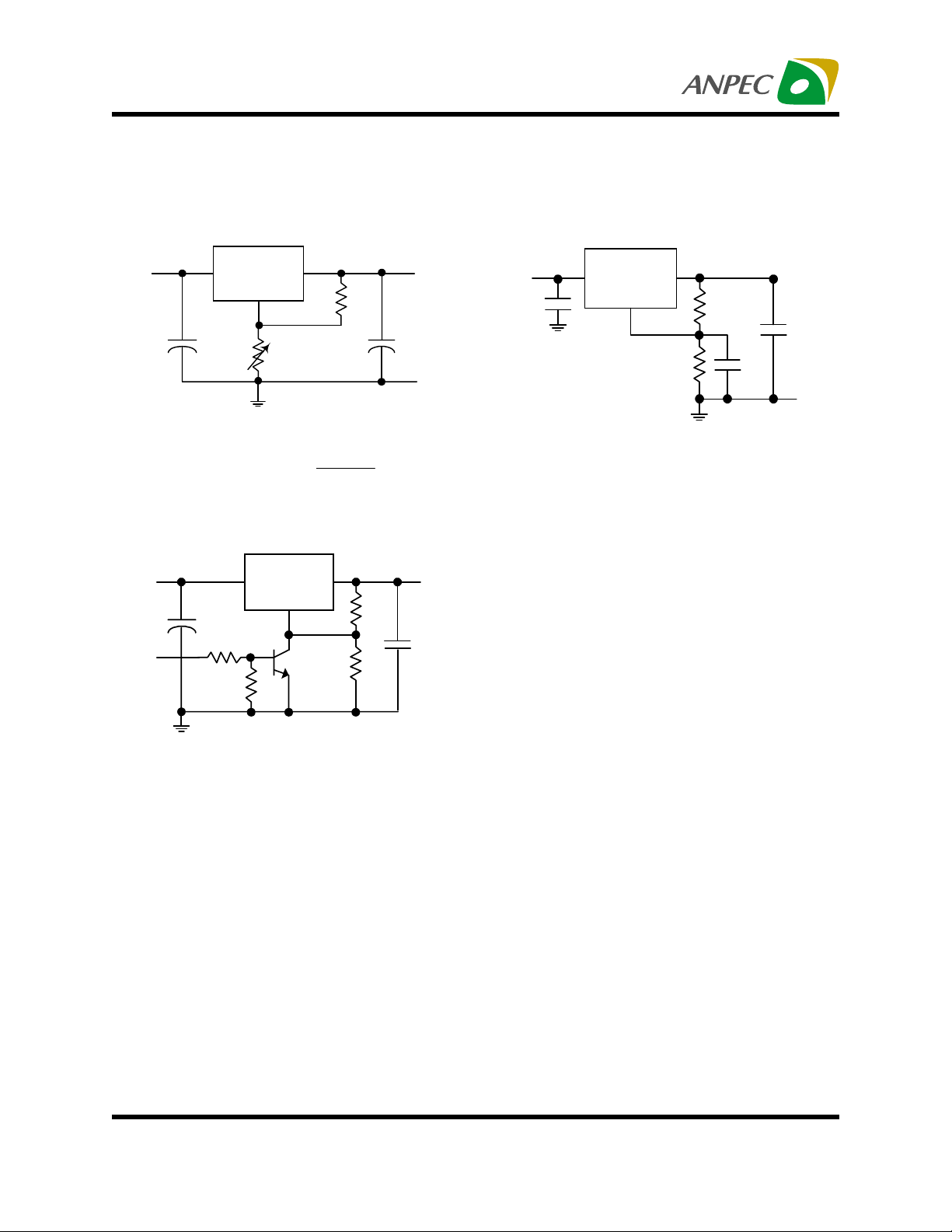
1.25V to 10.7V Adjustable Regulator Impro ving Ripple Rejection
V
IN
+
* Needed if device is far from filter capacitors
APL1117
F
10µ
C
1*
OUT
V
= 1.250V X
ADJ
OUTIN
R1
121
R2
1k
R1 + R2
5V Regulator with Shutdown
APL1117
V
IN
TTL
+
10µ
F
1k
OUTIN
ADJ
1k
V
OUT1
Ω
F
100µ
+
C
2
V
10µ
ADJ
OUTIN
R1
121
Ω
IN
+
F
1%
R2
365
Ω
C1
+
10µ
F
V
OUT
150µF
1%
APL1117
* C1 improves ripple rejection.
X
should be approximately
C
equal to R1 at ripple frequency
R1
5V
121
Ω
1%
365
+
Ω
100µ
F
1%
Copyright ANPEC Electronics Corp.
Rev. B.8 - Jun., 2003
5
www.anpec.com.tw
Page 6
APL1117
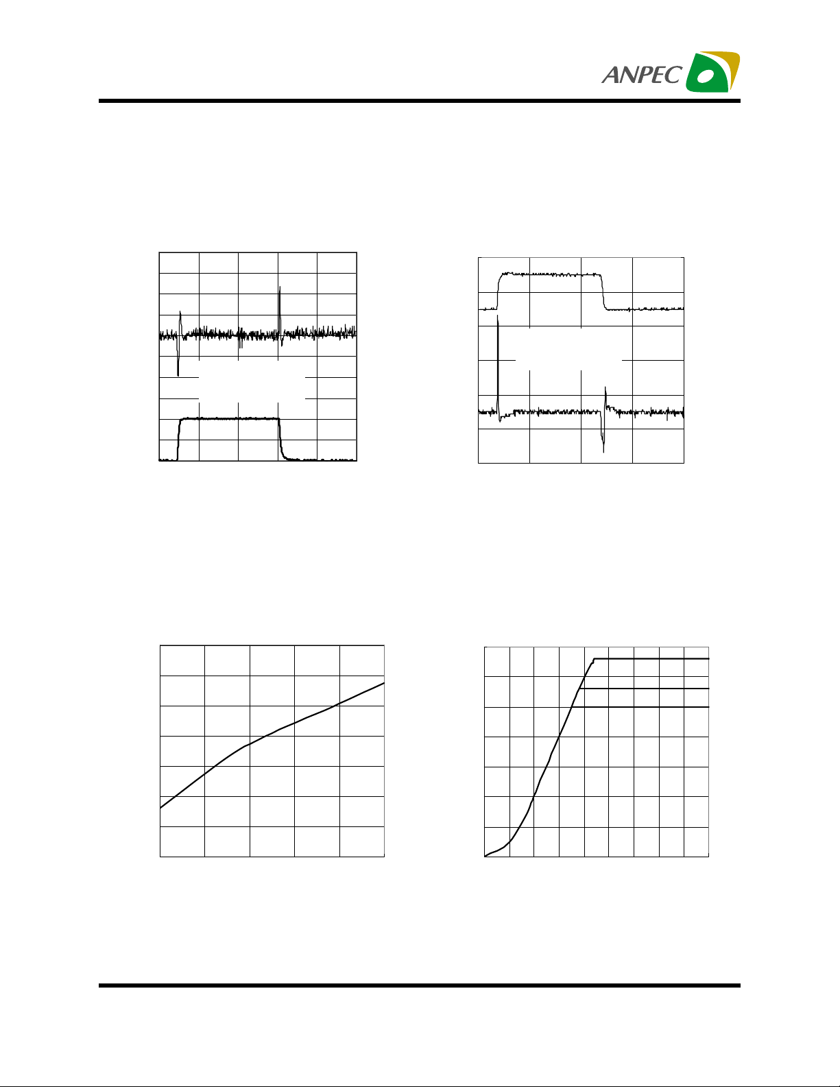
Typical Characteristics
Load Transietn Response
5
4.5
4
3.5
3
2.5
2
1.5
Output Current (A)
1
CIN=10µF
C
OUT=10µF T antalum
VIN=5V
0.5
0
-100 100 300 500 700 900
Time (µS)
Dropout Voltage vs. Output Current
1.25
APL1117-33
0.02
0.01
0
-0.01
-0.02
-0.03
APL1117-33
Line Transient Response
6
5
4
3
2
CIN=10µF
COUT=10µF T antalum
IOUT=0.1A
APL1117-33
Input Voltage (V)
1
0
-20 30 80 130 180
Time (µS)
Output Voltage vs. Input V oltage
3.5
0.15
0.1
0.05
0
-0.05
1.2
1.15
1.1
1.05
1
Dropout V oltage (V)
0.95
0.9
0 0.2 0.4 0.6 0.8 1
Output Current (A)
Copyright ANPEC Electronics Corp.
Rev. B.8 - Jun., 2003
6
3
2.5
2
1.5
1
Output Voltage (V)
0.5
0
0123456789
Input V oltage (V)
www.anpec.com.tw
Page 7

APL1117
Typical Characteristics Cont.
Input Current vs. Input Voltage
6
5
4
3
2
Input Current (mA)
1
0
024681012
Input V oltage (V)
Output Voltage vs. Temperature
2.6
2.5
2.4
2.3
2.2
2.1
2
1.9
Output Voltage (V)
1.8
1.7
1.6
-50 -25 0 25 50 75 100 125
Current Limit vs. Input Voltage
2.4
2.2
2
1.8
1.6
1.4
Current Limit (A)
1.2
1
5 7 9 11 13
APL1117-33APL1117-33
Input V oltage (V)
Output Voltage vs. Temperature
3.4
3.3
3.2
3.1
3
2.9
Output Voltage (V)
2.8
2.7
-50-250255075100125
T emperature (°C)
Copyright ANPEC Electronics Corp.
Rev. B.8 - Jun., 2003
Temperature (°C)
7
www.anpec.com.tw
Page 8

APL1117
Typical Characteristics Cont.
Adjustable Pin Current vs. T emperature
70
68
66
64
62
60
58
56
54
52
Adjustable Pin Current (µA)
50
-50 -25 0 25 50 75 100 125
Temperature (°C)
Current Limit vs. Temperature
1.9
1.8
1.7
1.6
1.5
1.4
1.3
Current Limit (A)
1.2
1.1
1
-50 0 50 100 150
VIN-VOUT=5V
APL1117-Adj
APL1117-33
Input Current vs. Tmeperature
8
7
6
5
4
APL1117-33
Input Current (mA)
3
2
-50 -25 0 25 50 75 100 125
Temperature (°C)
PSRR vs. Frequency
+0
Cadj=22µF
-10
IOUT=0.1A
Vripple=1Vp-p
-20
-30
-40
-50
-60
PSRR (dB)
-70
-80
-90
-100
10
20
VIN-VOUT>=Vdropout
VIN-VOUT>=3V
50 100 200 500 1k 2k 5k
10k 20k
50k
APL1117-33
200k
T emperature (°C)
Copyright ANPEC Electronics Corp.
$
Rev. B.8 - Jun., 2003
Frequency (Hz)
8
www.anpec.com.tw
Page 9

APL1117
Application Information
Output Voltage
The APL1117 develops a 1.25V reference voltage
between the output and the adjust terminal. By placing a resistor between these two terminals, a constant Current is caused to flow through R1 and down
through R2 to set the overall output voltage. Normally
this current is chosen to be the specified minimum
load current of 10mA. For fixed voltage devices R1
and R2 are included in the device.
OUT
APL1117
I
ADJ
60µA
= V
OUTIN
ADJ
REF
(1+ )+ I
R2
R1
ADJ
V
R2
REF
R1
R2
V
OUT
V
IN
V
Figure 1. Basic Adjustable Regulator
Rp
V
IN
APL1117
OUTIN
ADJ
PAR A SIT IC
LINE RESISTANCE
R1
CONNECT
R1 TO CASE
R2
CONNECT
R2 TO LOAD
R
Figure 2. Connections for Best Load Regulation
Input Capacitor
An input capacitor of 10µF or greater is
recommended. Tantalum, or aluminum electrolytic
capacitors can be used for bypassing. Larger Values will improve ripple rejection by bypassing the in-
L
Load Regulation
When the adjustable regulator is used. Load regulation will be limited by the resistance of the wire connecting the regulator to the load. The data sheet specification for load regulation is measured at the output
pin of the device. Best load regulation is obtained
when the top of the resistor divider (R1) is tied directly to the output pin of the device, not to the load.
For fixed voltage devices the top of R1 is internally
connected to the output, and the ground pin can be
connected to low side of the load. If R1 were connected to the load, RP is multiplied by the divider
ratio, the effective resistance between the regulator
and the load would be:
Rp X (1+ ), Rp = Parasitic L ine Resistance
R2
R1
put to the regulator.
Output Capacitor
The APL1117 requires an output capacitor to maintain stability and improve transient response. Proper
capacitor selection is important to ensure proper
operation. The APL1117 output capacitor selection
is dependent upon the ESR (equivalent series
resistance) of the output capacitor to maintain stability.
When the output capacitor is 10uF or greater, the
output capacitor should have an ESR less than 1Ω.
This will improve transient response as well as promote stability. A low-ESR solid tantalum capacitor
works extremely well and provides good transient response and stability over temperature.
Copyright ANPEC Electronics Corp.
Rev. B.8 - Jun., 2003
9
www.anpec.com.tw
Page 10

APL1117
Application Information (Cont.)
Output Capacitor (Cont.)
Aluminum electrolytics can also be used, as long as
the ESR of the capacitor is <1Ω. The value of the
output capacitor can be increased without limit. Higher
capacitance values help to improve transient response
and ripple rejection and reduce output noise.
Ripple Rejection
The curves for Ripple Rejection were generated using an adjustable device with the adjust pin bypassed.
With a 22µF bypassing capacitor 75dB ripple rejection is obtainable at any output level. The impedance
of the adjust pin capacitor, at the ripple frequency,
should be < R1. R1 is normally in the range of 100Ω-
200Ω. The size of the required adjust pin capacitor
is a function of the input ripple frequency. At 120Hz,
with R1=100Ω, the adjust pin capacitor should be
13µF. For fixed voltage devices, and adjustable de-
Figure 3&4 shows for the TO-252 and SOT-223 the
measured values of θ(J-A) for different copper area
sizes using a 2 layers, 1.6mm, and 6Sq. cm FR-4
PCB with 2oz. copper and a ground plane layer on
the backside area used for heatsinking. It can be
used as a rough guideline in estimating thermal
resistance.
50
TA=25°C
45
40
35
Thermal Resistance
30
(Juntion to Ambient) (°C/W)
25
02468101214
Top Copper Area (cm2)
vices without an adjust pin capacitor, the output ripple
will increase as the ratio of the output voltage to the
reference voltage (VOUT /VREF ).
Thermal Considerations
APL1117 has thermal protection which limits junction
temperature to 150°C. However, device functionality
is only guaranteed to a maximum junction temperature of +125°C.
Both the TO-220, TO-252, TO-263 and SOT-223
packages use a copper plane on the PCB and the
PCB itself as a heatsink. To optimize the heat sinking
ability of the plane and PCB, solder the tab of the
package to the plane.
Copyright ANPEC Electronics Corp.
Rev. B.8 - Jun., 2003
Figure 3.
θ(J-A) vs. copper area for the SOT-252 package
10
www.anpec.com.tw
Page 11

APL1117
Application Information (Cont.)
Thermal Considerations (Cont.)
60
TA=25°C
55
50
45
40
Thermal Resistance
35
(Juntion to Ambient) (°C/W)
30
0 2 4 6 8 10 12 14
Top Copper Area (cm2)
Figure 4.
θ(J-A) vs. copper area for the SOT-223 package
The thermal resistance for each application will be
affected by thermal interactions with other components on the board. Some experimentation will be
necessary to determine the actual value.
The power dissipation of APL1 117 is equal to :
PD = (VIN - VOUT) x IOUT
Maximum junction temperature is equal to :
TJUNCTION = TAMBIENT + (PD x θJA)
Note: TJUNCTION must not exceed 125°C
Copyright ANPEC Electronics Corp.
Rev. B.8 - Jun., 2003
11
www.anpec.com.tw
Page 12

APL1117
Package Information
TO-220 ( Reference JEDEC Registration TO-220)
D
Q
R
E
L1
b
e
b1
e1
H1
A
F
L
c
J1
Millimeters Inches
Dim
Min. Max. Min. Max.
A 3.56 4.8 3 0.1 4 0 0.19 0
b1 1.14 1.78 0.04 5 0.070
b 0.51 1.14 0.0 2 0 0.04 5
c 0.31 1 .14 0 .012 0.045
D 14.23 16.51 0.560 0.650
e 2.29 2.79 0.0 9 0 0 .110
e1 4.83 5.33 0.19 0 0.210
E 9.65 10.67 0.380 0.420
F 0.51 1.40 0.02 0 0.05 5
H1 5.84 6.86 0.230 0.270
J1 2.03 2.92 0.080 0.115
L 12.7 14.73 0.500 0.580
L1 3.65 6.35 0.14 3 0.250
R 3.53 4 .09 0.1 3 9 0.16 1
Q 2.54 3.43 0.1 0 0 0.13 5
Copyright ANPEC Electronics Corp.
Rev. B.8 - Jun., 2003
12
www.anpec.com.tw
Page 13

APL1117
Package Informaion
TO-252( Reference JEDEC Registration TO-252)
E
b2
L2
L1
A
C1
D
H
L
Dim
b
e1
D1
E1
Millimeters Inches
Min. Max. Min. Max.
C
A1
A 2.18 2.39 0.086 0.094
A1 0.89 1.27 0.035 0.050
b 0.508 0.89 0. 020 0.035
b2 5.2 07 5.461 0.205 0. 215
C 0.46 0.58 0.018 0.023
C1 0.46 0.58 0.018 0.023
D 5.334 6.2 2 0.210 0.2 45
D1 5.2 REF 0.205 REF
E 6.35 6.73 0.250 0.265
E1 5.3 REF 0.2 09 REF
e1 3.96 5.18 0.156 0.204
H 9.398 10.41 0.370 0.410
L 0.51 0.020
L1 0.64 1.02 0.025 0.040
L2 0.89 2.032 0.035 0. 080
Copyright ANPEC Electronics Corp.
Rev. B.8 - Jun., 2003
13
www.anpec.com.tw
Page 14

APL1117
Package Information
TO-263 ( Reference JEDEC Registration TO-263)
E
e
e1
A
c
c2
b2
b
L2
D
L
L3
Φ 1
L4
R
L1
DE T A IL "A "R O T E D
E1
TERMINAL 4
D1
Millim e t er s Inch e s
Dim
Min. Max. Min. Max.
A 4.06 4.83 0.160 0.190
b
0.51 1.016
0.02 0.040
b2 1.14 1.651 0.045 0.065
c 0.38 TYP. 0.015 TYP.
c2
1.14 1.40
0.045 0.055
D 8.64 9.65 0.340 0.380
e 9.65 10.54 0.380 0.415
e1
2.54 TYP
0.100 TYP
L 14.60 15.88 0.575 0.625
L1 2.24 2.84 0.090 0.110
L2
1.02 2.92
0.040 0.112
L3 1.20 1.78 0.050 0.070
Copyright ANPEC Electronics Corp.
Rev. B.8 - Jun., 2003
14
www.anpec.com.tw
Page 15

APL1117
Package Information
SOT-223( Reference JEDEC Registration SOT-223)
D
B1
H E
K
e
e1
B
A
A1
b
a
c
L
Millimeters InchesDim
Min. Max. Min. Max.
A 1.50 1.80 0.06 0.07
A1 0.02 0.08
B 0.60 0.80 0.02 0.03
B1 2.90 3.10 0.11 0.12
c 0.28 0.32 0.01 0.01
D 6.30 6.70 0.25 0.26
E 3.30 3.70 0.13 0.15
e 2.3 BSC 0.09 BSC
e1 4.6 BSC 0.18 BSC
H 6.70 7.30 0.26 0.29
L 0.91 1.10 0.04 0.04
K 1.50 2.00 0.06 0.08
α
β
Copyright ANPEC Electronics Corp.
Rev. B.8 - Jun., 2003
0
°
13
°
10
°
15
0
°
13
10
°
°
www.anpec.com.tw
Page 16

APL1117
Physical Specifications
Terminal Material Solder-Plated Copper (Solder Material : 90/10 or 63/37 SnPb
Lead Solderability Meets EIA Specification RSI86-91, ANSI/J-STD-002 Category 3.
Packaging 2500 devices per reel
Reflow Condition (IR/Convection or VPR Reflow)
Reference JEDEC Standard J-STD-020A APRIL 1999
Peak temperature
temperature
Pre-heat temperature
°
183 C
Time
Classification Reflow Profiles
Convection or IR/
Convection
Average ramp-up rate(183°C to Peak) 3°C/second max. 10°C /second max.
Preheat temperature 125± 25°C)
°
Temperature maintained above 183
Time within 5°C of actual peak temperature
Peak temperature range
Ramp-down rate
Time 25°C to peak temperature
C
120 seconds max.
60 ~ 150 seconds
10 ~ 20 seconds
°
220 +5/-0
°
C /second max. 10°C /second max.
6
6 minutes max.
C or 235 +5/-0°C 215~ 219°C or 235 +5/-0°C
60 seconds
VPR
Package Reflow Conditions
pkg. thickness
and all bags
Convection 220 +5/-0°C
VPR 215-219°C
IR/Convection 220 +5/-0
Copyright ANPEC Electronics Corp.
Rev. B.8 - Jun., 2003
2.5mm
≥≥≥≥
°
C IR/Convection 235 +5/-0
pkg. thickness < 2.5mm and
pkg. volume
≥≥≥≥
350 mm
16
pkg. thickness < 2.5mm and pkg.
volume <
°
Convection 235 +5/-0
VPR 235 +5/-0
°
C
C
°
C
www.anpec.com.tw
Page 17

APL1117
Re lia bility test p r o gram
Test item Method Description
SOLDERABILITY M IL-STD-883D-2003
HOLT MIL-STD-883D-1005.7
PCT JESD-22-B, A102
TST MIL-STD-883D-1011.9
ESD MIL-STD-883D-3015.7 VHBM > 2KV, VMM > 200V
Latch-Up JESD 78 10ms , Itr > 100mA
245°C , 5 SEC
1000 Hrs Bias @ 125 °C
168 Hrs, 100 % RH , 121°C
-65°C ~ 150°C, 200 Cycles
Carrier Tape & Reel Dimension
P
P1
Ao
J
C
W
E
Po
F
A
D
D1
t
Bo
Ko
T2
B
T1
Applica tio n
TO-252
Applica tio n
TO-263
Applica tio n
SOT-223
Copyright ANPEC Electronics Corp.
Rev. B.8 - Jun., 2003
A B C J T1 T2 W P E
330 ±3100 ± 213 ± 0. 5 2 ± 0.5
F D D1 Po P1 Ao Bo Ko t
7.5 ± 0 .1 1 .5 + 0 .1 1.5± 0.25 4.0 ± 0.1 2.0 ± 0 .1 6 .8 ± 0.1 10.4± 0 .1 2 .5± 0.1 0.3±0.05
A B C J T1 T2 W P E
380±380 ± 213 ± 0. 5 2 ± 0.5 24 ± 42± 0.3
F D D1 Po P1 Ao Bo Ko t
11 .5 ± 0 .1 1 .5 + 0 .1 1.5± 0.25 4.0 ± 0.1 2.0 ± 0.1 10.8 ± 0.1 16.1± 0 .1 5 .2± 0.1
A B C J T1 T2 W P E
330±162±1.5
F D D1 Po P1 Ao Bo Ko t
5.5 ± 0.05 1.5+ 0.1 1.5+ 0.1 4.0 ± 0 .1 2.0 ± 0.05 6.9 ± 0 .1 7 .5± 0 .1 2 .1± 0.1 0.3±0.05
12.75
0.15
16.4 + 0.3
-0.2
±
2 ± 0.6 12.4 +0.2 2± 0.2 12 ± 0.3 8 ± 0 .1 1 .7 5± 0.1
17
2.5± 0.5
16+ 0.3
- 0.1
24 + 0.3
- 0.1
8 ± 0.1
16 ± 0.1 1.75± 0.1
www.anpec.com.tw
1.75± 0.1
0.35±0.01
3
Page 18

APL1117
Cover Tape Dimensions
Application Carrier Width Cover Tape Width Devices Per Reel
TO- 252
TO- 263
SOT- 223
Customer Service
Anpec Electronics Corp.
Head Office :
5F, No. 2 Li-Hsin Road, SBIP,
Hsin-Chu, Taiwan, R.O.C.
Tel : 886-3-5642000
Fax : 886-3-5642050
Taipei Branch :
7F, No. 137, Lane 235, Pac Chiao Rd.,
Hsin Tien City, Taipei Hsien, Taiwan, R. O. C.
Tel : 886-2-89191368
Fax : 886-2-89191369
16 13.3 2500
24 21.3 1000
12 9.3 2500
Copyright ANPEC Electronics Corp.
Rev. B.8 - Jun., 2003
18
www.anpec.com.tw
 Loading...