

Page 1
APLUS INTEGRATED CIRCUITS INC.
API860G
GENERAL DESCRIPTION :
API860G is 63 seconds single chip high quality voice synthesizer IC which contains one 4-bit
Input port, three 4-bit I/O ports and a 4 bits CPU controller. By programming through the 4 bits CPU
controller, user's application includes section combination, trigger mode, control outputs, keyboard
matrix and other logic function can be easily implemented.
FEATURES :
• Single power supply.
• Crystal/Ring oscillator option.
• 63 seconds voice capacity.
• I/O port : 4 I + 12 I / O (But only P1 and P2 can wake up)
• Power down mode for saving power consumption.
• Reset pin available.
• Single ROM for voice program. Maximum 32 K program addressing size available.
• Readable ROM data.
• One 6 bit timer overflow control is provided.
• Two stack for subroutine call.
• 5 bits ASPCM synthesis.
• 38K Hz modulation for IR transmission.
• 15 steps volume control.
• Direct Drive/traditional DAC.
• 8 bits resolution D/A.
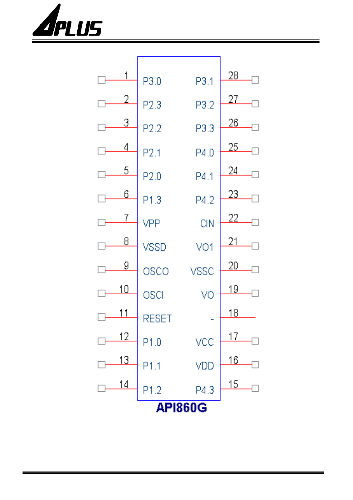
PIN DESCRIPTIONS :
Symbol I/O Function
P1.0
P1.1
P1.2
P1.3
P2.0
P2.1
P2.2
P2.3
P3.0
P3.1 I/O Bit 1 of Port 3.
P3.2 I/O Bit 2 of Port 3. The pin can generate 38KHz square wave.
P3.3 I/O Bit 3 of Port 3. The pin can be treated as an LED output flashing with volume
P4.0
P4.1
P4.2
P4.3
VDD I
OSCI I Ring oscillator/crystal input pin.
RESET I Reset Pin.
OSCO O Crystal output pin.
TEST I For testing only.
VSSD I Negative digital power supply.
VCC I Positive analog power supply.
VSSC I Negative analog power supply.
VO O Constant current output / Push Pull voice output.
VO1 O Push Pull voice output.
I
Bit 0 of Port 1.
I
Bit 1 of Port 1.
I
Bit 2 of Port 1.
I
Bit 3 of Port 1.
I/O Bit 0 of Port 2.
I/O Bit 1 of Port 2.
I/O Bit 2 of Port 2.
I/O Bit 3 of Port 2.
I/O Bit 0 of Port 3.
I/O Bit 0 of Port 4
I/O Bit 0 of Port 4
I/O Bit 0 of Port 4
I/O Bit 0 of Port 4
Positive digital power supply.
1
http:// www.aplusinc.com.tw
Page 2
APLUS INTEGRATED CIRCUITS INC.
API860G
2
http:// www.aplusinc.com.tw
Page 3

APLUS INTEGRATED CIRCUITS INC.
API860G
ABSOLUTE MAXIMUM RATINGS :
Items Sym. Min. Max. Unit
Supply Voltage VDD-VSS -0.3 6.0 V
Input Voltage VIN VSS -0.3 VDD+0.3 V
Operating Temperature TOP 0.0 70.0 oC
Storage Temperature TSTG -25.0 +125.0 oC
ELECTRICAL CHARACTERISTICS
Parameter Sym. Min. Typ. Max. Unit Condition
Operating voltage VDD 2.4 3.0 5.1 V
Standby current IDDS - - 2.0 µA VDD=3V
Operating current IDDO - 180 350 µA
Operating current IDDO - 3 6 mA
Drive current of
P2,P3,P4
Sink current of P2
(before KEYB)
Sink current of P2
(after KEYB)
IOD 2.0 3.0 - mA VDD=3V, VO=2.4V
IOS - 3.0 10.0 µA VDD=3V, VO=3V
IOS 2.3 3.5 - mA VDD=3V, VO=0.4V
Sink current of P3,P4 IOS 2.3 3.5 - mA VDD=3V, VO=0.4V
Input current of P1 IIH - 3.0 10.0 µA VDD=3V
Output current of VO IVO
Output current of
VO,VO1
120 150 - mA VDD IVO =3V, VO=V1=0.7V
Oscillation resistor R -
4.0 5.0 6.4 mA VDD=3V, VO=0.7V
4.0 5.3 6.7 mA VDD=4.5V, VO=0.7V
470 - KΩ VDD=3V
100 - KΩ VDD=3V
Oscillation frequency FOSC 1.08 1.2 1.32 MHz VDD=2.2~5.5V
(25oC, VDD=3.0 Volts unless otherwise specified)
VDD=3V, No load,
constant current D/A operate
VDD=3V, No load,
push-pull current D/A operate
APPLICATION CIRCUIT :
In the following application circuits:
*1 : For heavy loading application, adding an electrolytic capacitor between Vcc and Ground
is recommended.
The recommended value for button cell application is 10µF.
*2 : The recommended value for button cell application is 750,or less.
3
http:// www.aplusinc.com.tw
Page 4

APLUS INTEGRATED CIRCUITS INC.
20-key Application Circuit
API860G
64-key Application Circuit
4
http:// www.aplusinc.com.tw
Page 5

APLUS INTEGRATED CIRCUITS INC.
connect board
Download board operation :
1. Connect to the PC print port .
API860G
2.
Put a API860G IC on the socket .
3.
Power supple: 15V.
4. Turn on the power sw .
5.
Press the programming button to
burn the IC .
(Use the MTP Writer software.)
15 V
Power sw
API860G
To PC print port
5
http:// www.aplusinc.com.tw
 Loading...