

Page 1

PLUS MAKE YOUR PRODUCTION A-PLUS
A
APExx16 Series
DATA SHEET
PLUS INTEGRATED CIRCUITS INC.
A
Address:
3 F-10, No. 32, Sec. 1, Chenggung Rd., Taipei,
Taiwan 115, R.O.C.
(115)台北市南港區成功路㆒段 32 號 3 樓之 10.
TEL: 886-2-2782-9266
FAX: 886-2-2782-9255
WEBSITE : http: //www.aplusinc.com.tw
Sales E-mail:
sales@aplusinc.com.tw
Technology E-mail:
service@aplusinc.com.tw
Page 2
APExx16 Series
1.0 General Description
The APExx16 series are very low cost voice and melody synthesizer with 4-bits CPU. They have various
features including 4-bits ALU, ROM, RAM, I/O ports, timers, clock generator, voice and melody
synthesizer, and PWM (Direct drive) or D/A current outputs, etc. The audio synthesizer contains one
voice-channel and two melody-channels. Furthermore, they consist of 27 instructions in these devices.
With CMOS technology and halt function can minimize power dissipation. Their architectures are similar
to RISC, with two stages of instruction pipeline. They allow all instructions to be executed in a single
cycle, except for program branches and data table read instructions (which need two instruction cycles).
2.0 Features
(1) Single power supply can operate from 2.4V to 5.5V at 4MHz or 8MHz.
(2) Program ROM: 16k x 10 bits ( APE8416 /APE10616 /APE12716 are 64k x 10 bits )
(3) 1 set of 16-bits DPR can access up to 64k x 10 bits melody data memory space, and 1 set of 19-bits
VPR can access up to 512k x 10 bits voice data memory space.
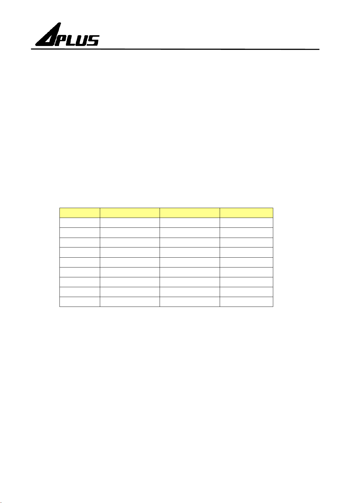
Product Voice Duration (sec) Voice Pointer (VPR) ROM Size (10-bits)
APE1016 10 15-bits 32k
APE1516 15 16-bits 48k
APE2016 20 16-bits 64k
APE3116 31 17-bits 96k
APE4116 41 17-bits 128k
APE6316 63 18-bits 192k
APE8416 84 18-bits 256k
APE10616 106 19-bits 320k
APE12716 127 19-bits 384k
(4) Data Registers:
a). 128 x 4-bits data RAM (00-7Fh)
b). Unbanked special function registers (SFR) range: 00h-2Fh
(5) I/O Ports:
a). PRA: 4-bits I/O Port A (10h) can be programmed to input/output individually. (Regist er control)
b). PRB: 4-bits I/O Port B (13h) can be configured to input/output individually. (Mask option)
c). PR C: 4-bits I/O Port C (14h) can be programmed to input/output individually. (Register control)
d). PRD: 4-bits I/O Port D (15h) can be programmed to input/output individually. (Register control)
(6) On-chip clock generator: Resistive Clock Drive
(7) Timer: 1-set Voice Interrupt (Timer0: a 9-bits auto-reload timer/counter).
(8) Stack: 2-level subroutine nesting.
(9) B uilt-in 4 Level Vol u me C ontrol can be prog r amm ed .
1
or Crystal oscillator
(RM)
(HM)
Rev 1.1 2003/9/2
Page 3
APExx16 Series
(10) Built-in 8 Level DAC current output can be configured. (Mask option)
(11) Built-in IR Carry Output: Port B[1] can be configured as IR pin by 38k / 56kHz. (Mask option)
(12) External Reset: Port B[3] can be configured as reset pin. (Mask opt on)
(13) HALT and Release from HALT function to reduce power consumpt ion
(14) Watch Dog Timer (WDT)
(15) Instruction: 1-cycle instruction except for table read and program branches which are 2-cycles
(16) Number of instruction: 27
(17) DAC: 1 channel voice and dual tone melody synthesizer (One 9-bits Cout or 8-bits PWM output).
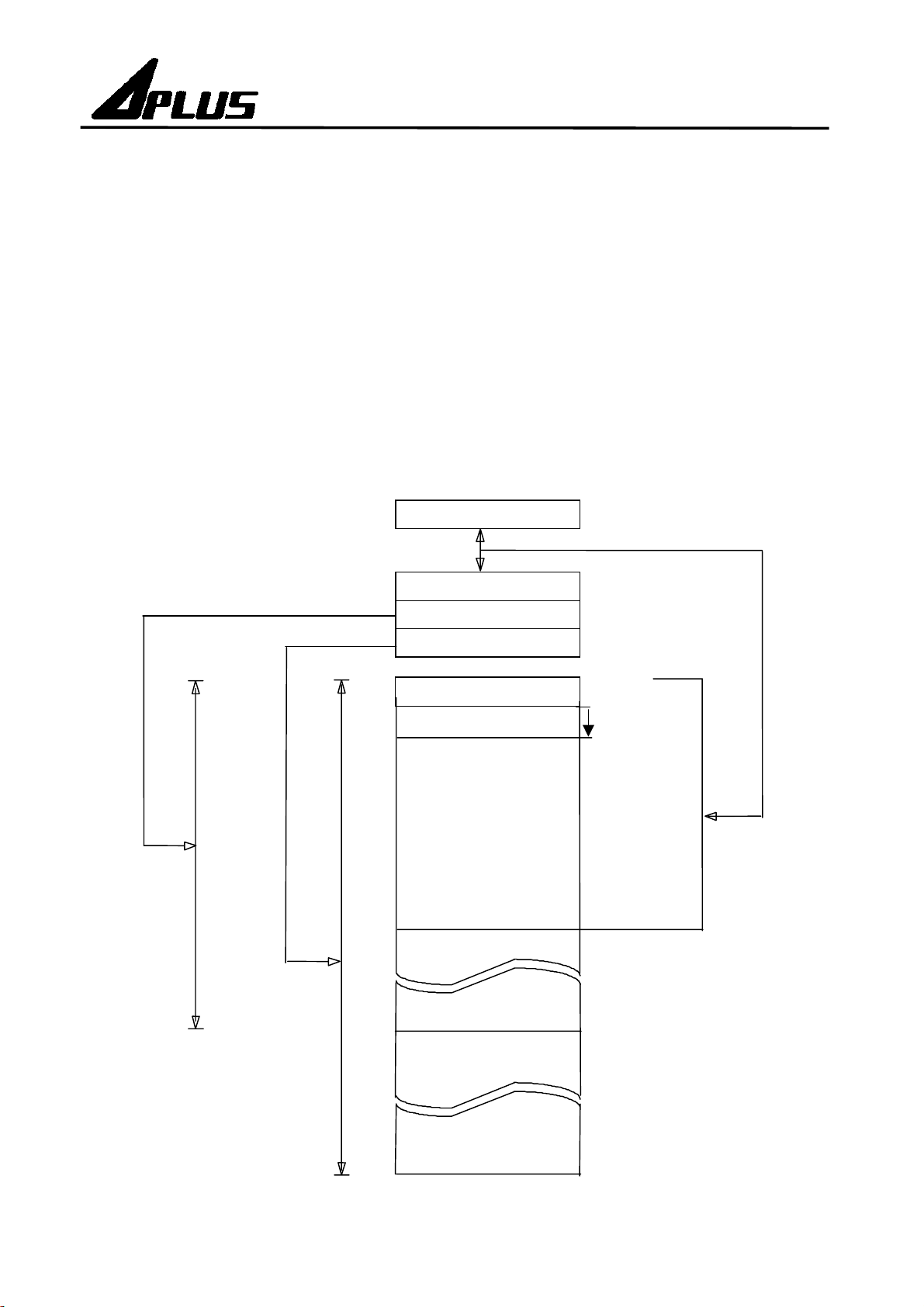
FIGURE 1 : ROM Map of APExx16 Series
00000h-0FFFFh
Data ROM for Melody
PC[13:0]
14-bit x 2 STACK
16-bit Data Pointer
19-bit Voice Pointer
Reserved for Test ing
Reset Vector
00000h
000FEh
000FFh-00400h
00401h
00000h-03FFFh
Program ROM
00000h-7FFFFh
Voice RO M for Vo ice
2
* APE8416 /APE10616 /APE12716 are 64k x 10 bits
Rev 1.1 2003/9/2
Page 4

3.0 Pin Description
Pad Name Pin Attr. Description
PWM2/Cout
PWM1
Vdd1~3
PRA0~3
PRC0~3
PRD0~3
PRB0 / OSC2
PRB1 / IR
PRB2
PRB3 / Reset
OSC1
GND1~4
Power
Power
O
O PWM1 output.
I/O
I/O
I/O
I/O
I/O
I
PWM2 output, or Current Output of Audio.
Power supply during operation.
I/O port can be programmed to input/output individually.
Input type with weak pull-low or fix-input-floating capability.
Buffer Output type.
I/O port can be configured to input/output individually or HM OSC pad.
Input type with weak pull-low or fix-input-floating capability.
Buffer Output type.
I/O port can be configured to input/output individually.
Input type with weak pull-low or fix-input-floating capability.
Buffer Output type.
Mask option selected as an IR Carrier Output with 38k / 56kHz
I/O port can be configured to input/output individually.
Input type with weak pull-low or fix-input-floating capability.
Buffer Output type.
I/O port can be configured to input/output individually.
Input type with weak pull-low or fix-input-floating capability.
Buffer Output type.
Mask option selected as an external RESET pin with weak pull-low
capability.
RM/HM mode Oscillator input
Ground Potential
APExx16 Series
4.0 DC Characteristics
Symbol Parameter Vdd Min. Typ. Max. Unit Condition
Vdd Operating voltage 2.4 3 5.5 V depending on Freq.
Isb Standby
Iop
Iih
Ioh Output-high current
Iol Output-low current
Cout
dF/F Frequency stability -5 5 %
dF/F Fosc lot variation -10 10 %
Supply
current
Input current
(Inter n al pu l l lo w)
DAC output current
(8-level option)
Operating
3 1
4.5 1
3 2
4.5 7
3 3
4.5 10
3 -3
4.5 -10
3 7
4.5 19
3 0.8 ~ 4.8
4.5 0.9 ~ 6.5
uA
mA
uA
mA
mA
4MHz, RM,
in HALT Mode
4MHz, RM,
IO Floating
Input ports with weak
pull-low
4MHz, RM
(IO ports)
4MHz, RM
(Full s cale)
Fosc(3v- 2.4v)
Fosc (3v)
Vdd=3V, Rosc=180k,
4MHz
3
Rev 1.1 2003/9/2
Page 5

APExx16 Series
FIGURE 2 : Frequency vs. Rosc (at 3V)
Resistor (Rosc ohms) 110k 200k 300k 430k
Frequency (MHz)
20
15
14.84 8.25 5.54 3.92
Rosc vs Freq.
14.84
10
Freq. (MHz)
5
0
0 100 200 300 400 500
5.0 Application Circuit
8.25
Rosc (k ohm)
5.54
3.92
4
Rev 1.1 2003/9/2
Page 6

6.0 Bonding Diagram of APE1016 /APE1516 /APE2016
X
Y
APExx16 Series
25
GND1
PRD0
24
ROM
PRD1
PRD2
PRD3
PRC0
23
22
21
20
Vdd3 1
Chip Size : 1432 um x 1650 um
Pad Size : 80 um x 80 um
* The IC substrate must be connected to GND.
2
PWM2/Cout
Vdd2
3
PWM1
4
GND3
5
PRA3
PRA2
6 7
PRA1
8
PRA0
PRB3
PRB2
9
10
11
PRC1
PRC2
PRC3
PRB0
OSC1
GND2
PRB1
12
19
18
17
16
15
14
Vdd1
13
(0,0)
Pad # Pad Name X Y Pad # Pad Name X Y
1
2
3
4
5
6
7
8
9
10
11
12
13
Vdd3 56 647
PWM2/Cout 58 466
Vdd2 58 182
PWM1 145 58
GND3 293 58
PRA3 413 87
PRA2 533 87
PRA1 653 87
PRA0 773 87
PRB3/Reset 893 87
PRB2 1013 87
PRB1/IR 1133 87
Vdd1 1253 87
5
14
15
16
17
18
19
20
21
22
23
24
25
GND2 1261 235
OSC1 1261 350
PRB0/OSC2 1261 465
PRC3 1261 580
PRC2 1261 695
PRC1 1261 810
PRC0 1261 925
PRD3 1261 1040
PRD2 1261 1155
PRD1 1261 1270
PRD0 1261 1385
GND1 1261 1500
Rev 1.1 2003/9/2
Page 7

6.1 Bonding Diagram of APE3116 /APE4116 /APE6316
X
Y
APExx16 Series
GND1
25
PRD0
24
ROM
PRD1
PRD2
PRD3
PRC0
23
22
21
20
PRC1
PRC2
19
18
Chip Size : 1408 um x 2556 um
PRC3
Pad Size : 80 um x 80 um
* The IC substrate must be connected to GND.
PRB0
17
16
Vdd3 1
PWM2/Cout
2
OSC1
PRB1
15
14
(0,0)
Vdd2
3
PWM1
4
GND3
5
PRA3
PRA2
6 7
PRA1
8
PRA0
PRB3
10
9
GND2
PRB2
11
13
Vdd1
12
Pad # Pad Name X Y Pad # Pad Name X Y
1
2
3
4
5
6
7
8
9
10
11
12
13
Vdd3 56 647
PWM2/Cout 58 466
Vdd2 58 182
PWM1 145 58
GND3 293 58
PRA3 430 87
PRA2 563 87
PRA1 696 87
PRA0 829 87
PRB3/Reset 962 87
PRB2 1095 87
Vdd1 1228 87
GND2 1248 272
6
14
15
16
17
18
19
20
21
22
23
24
25
PRB1/IR 1248 405
OSC1 1248 570
PRB0/OSC2 1248 733
PRC3 1248 896
PRC2 1248 1056
PRC1 1248 1218
PRC0 1248 1379
PRD3 1248 1540
PRD2 1248 1700
PRD1 1248 1861
PRD0 1248 2022
GND1 1248 2310
Rev 1.1 2003/9/2
Page 8

APExx16 Series
X
Y
6.2 Bonding Diagram of APE8416 /APE10616 /APE12716
26
Vdd1
25
PRB3
24
PRC3
23
PRC2
22
PRC1
21
PRC0
20
PRD3
19
PRD2
18
PRD1
17
PRD0
16
GND1
ROM
Chip Size : 2288 um x 2364 um
Pad Size : 80 um x 80 um
* The IC substrate must be connected to GND.
1
2
3
1
2
3
4
5
6
7
8
9
10
11
12
13
GND4
GND3
PWM1
Vdd3
4
PWM2/Cout
5
Vdd2
6 7
GND4 76 404
GND3 59 294
PWM1 59 146
Vdd3 183 59
PWM2/Cout 467 59
Vdd2 815 76
OSC1 976 76
PRB0/OSC2 1140 76
PRB1/IR 1304 76
PRB2 1465 76
PRA0 1626 76
PRA1 1787 76
PRA2 1948 76
OSC1
PRB0
8
14
15
16
17
18
19
20
21
22
23
24
25
26
PRB1
PRB2
10
9 12
PRA1 PRA0
11
PRA3 2109 76
GND2 2128 212
GND1 1927 2204
PRD0 1765 2204
PRD1 1603 2204
PRD2 1441 2204
PRD3 1279 2204
PRC0 1117 2204
PRC1 955 2204
PRC2 739 2204
PRC3 631 2204
PRB3/Reset 469 2204
Vdd1 307 2204
(0,0)
Pad # Pad Name X Y Pad # Pad Name X Y
GND2
15
PRA3 PRA2
13 14
7
Rev 1.1 2003/9/2
 Loading...