

Page 1
APA4835
Stereo 2.8W Audio Power Amplifier with DC Volume Control
and Selectable Gain
Features General Description
•
Operating Voltage : 3.3V to 5V
• Stereo switchable bridged/single-ended
power amplifiers
• DC Volume Control Interface , 0dB to –105dB
• Low Supply Current , I
• Low Shutdown Current , I
= 13mA at Stereo BTL
DD
= 0.7µA
DD
• Bridge-Tied Load (BTL) or Single-Ended-(SE)
Modes Operation
• Output Power at 1% THD+N , V
DD
=5V
–2.2W/Ch (typ) into a 3 Ω Load
–2.0W/Ch (typ) into a 4 Ω Load
–1.2W/Ch (typ) into a 8 Ω Load
• Output Power at 10% THD+N , V
DD
=5V
–2.8W/Ch (typ) into a 3 Ω Load
–2.3W/Ch (typ) into a 4 Ω Load
–1.5W/Ch (typ) into a 8Ω Load
• Single-ended mode at 1.0% THD+N
–95mW/Ch (typ) into 32Ω Load
• Depop Circuitry Integrated
• System Beep Detect
• Thermal shutdown protection circuitry
The APA4835 is a monolithic integrated circuit , which
provides DC volume control , and a stereo bridged
audio power amplifiers capable of producing 2.8W
(2.2W) into 3Ω with less than 10% (1.0%) THD+N.
APA4835 includes a DC volume control , stereo
bridge-tied and single-ended audio power amplifiers
, stereo docking outputs , and a selectable gain control , that makes it optimally fittable for notebook PC
, multimedia monitors , and other portable
applications. The attenuator range of the volume
control in APA4835 is from 0dB (DC_Vol=0.7VDD) to
–105dB (DC_Vol=0V) with 32 steps. Both of the
depop circuitry and the thermal shutdown protection
circuitry are integrated in APA4835 , that reduces
pops and clicks noise during power up or shutdown
mode operation , and protects the chip from being
destroyed by over temperature failure. To simplify
the audio system design , APA4835 combines a stereo bridge-tied loads (BTL) mode for speaker drive
and a stereo single-end (SE) mode for headphone
drive into a single chip , where both modes are easily
switched by the SE/BTL input control pin signal. Besides the low supply current design to increase the
efficiency of the amplifiers , APA4835 also features a
shutdown function which keeps the supply current
only 0.7µA (typ).
Pin Description
• High supply voltage ripple rejection
• Low Crossover Distortion
• PC99 Compliant
• 28-pin TSSOP-P (with enhanced thermal pad)
power package available
Applications
• Notebook and Desktop Computers
• Multimedia Monitors
GND
SHUTDOWN
Gain Select
Mode
Mute
V
DC Vol
GND
Right Dock
Right In
Beep In
Left In
Left Dock
GND
DD
1
2
3
4
5
6
7
8
9
10
11
12
13
14
28
27
26
25
24
23
22
21
20
19
18
17
16
15
Right Out +
V
DD
Right Out Right Gain 2
Right Gain 1
GND
BYPASS
HP Sense
GND
Left Gain 1
Left Gain 2
Left Out V
DD
Left Out +
• Portable Applications
ANPEC reserves the right to make changes to improve reliability or manufacturability without notice, and advise
customers to obtain the latest version of relevant information to verify before placing orders.
Copyright ANPEC Electronics Corp.
Rev. A.7 - Mar., 2003
www.anpec.com.tw1
Page 2
APA4835
Ordering Information
APA4835
APA4835 R :
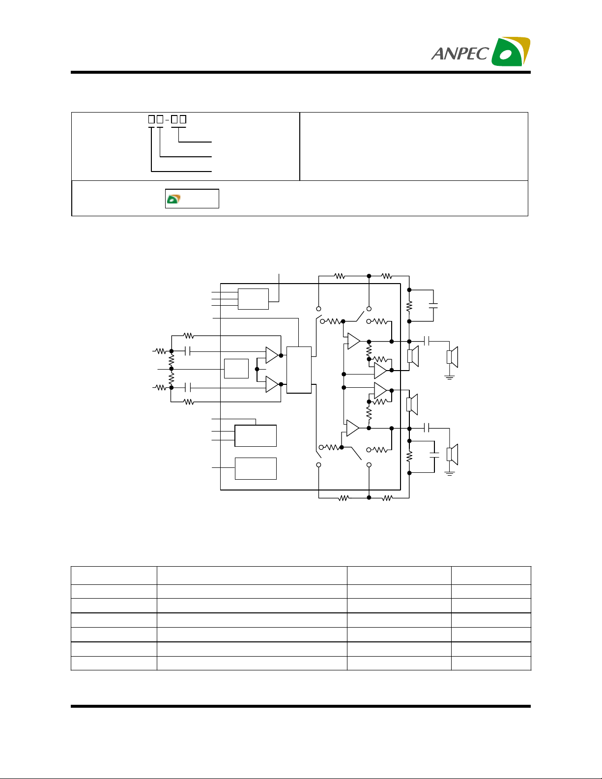
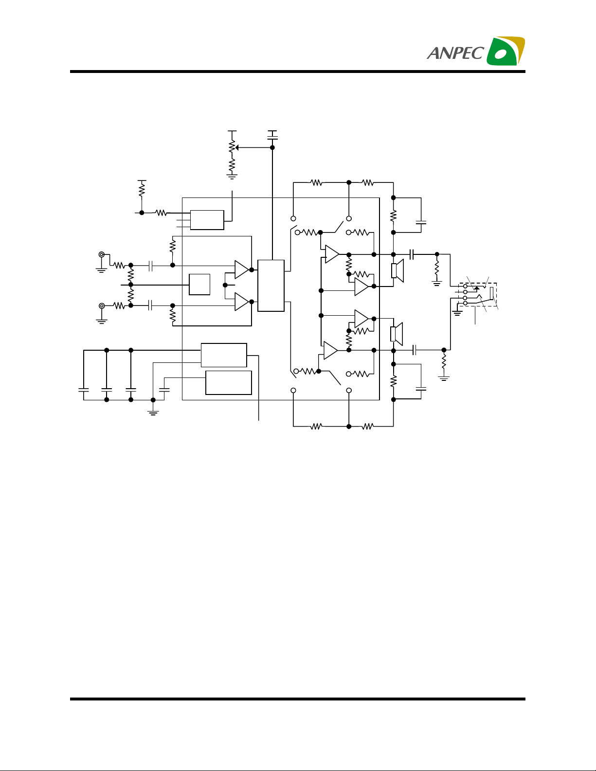
Block Diagram
DC Vol Control
Ω
20K
200K
Ω
200K
Ω
20K
Ω
APA4835
XXXXX
Mode
Mute
HP Sense
Left Dock
Ω
20K
Left In
µ
F
0.33
Beep In
µ
0.33
F
Right In
Right Dock
Ω
20K
Shutdown
V
DD
GND
Bypass
Handling Code
Temp. Range
Package C ode
Internal gain select
Mode
Control
Beep
Detect
Power
Management
Click and Pop
Suppression
Circuitry
+
Bias
+
-
Package C ode
R : T S S OP-P
Temp. Range
I : -40 to 85 C
Handling Code
TU : T u be TR : T a pe & R e e l
X X X X X - D a te Code
20K
10K
Ω
Volume
Control
32 steps
10K
Ω
°
Ω
-
+
20K
20K
+
20K
Ω
10K
Ω
Ω
20K
Ω
+
+
-
20K
Ω
Ω
10K
Ω
20K
Ω
- Left Out
+ Left Out
+ Right Out
- Right Out
Ω
20K
0.068µF
0.068µF
20K
Ω
20K
Ω
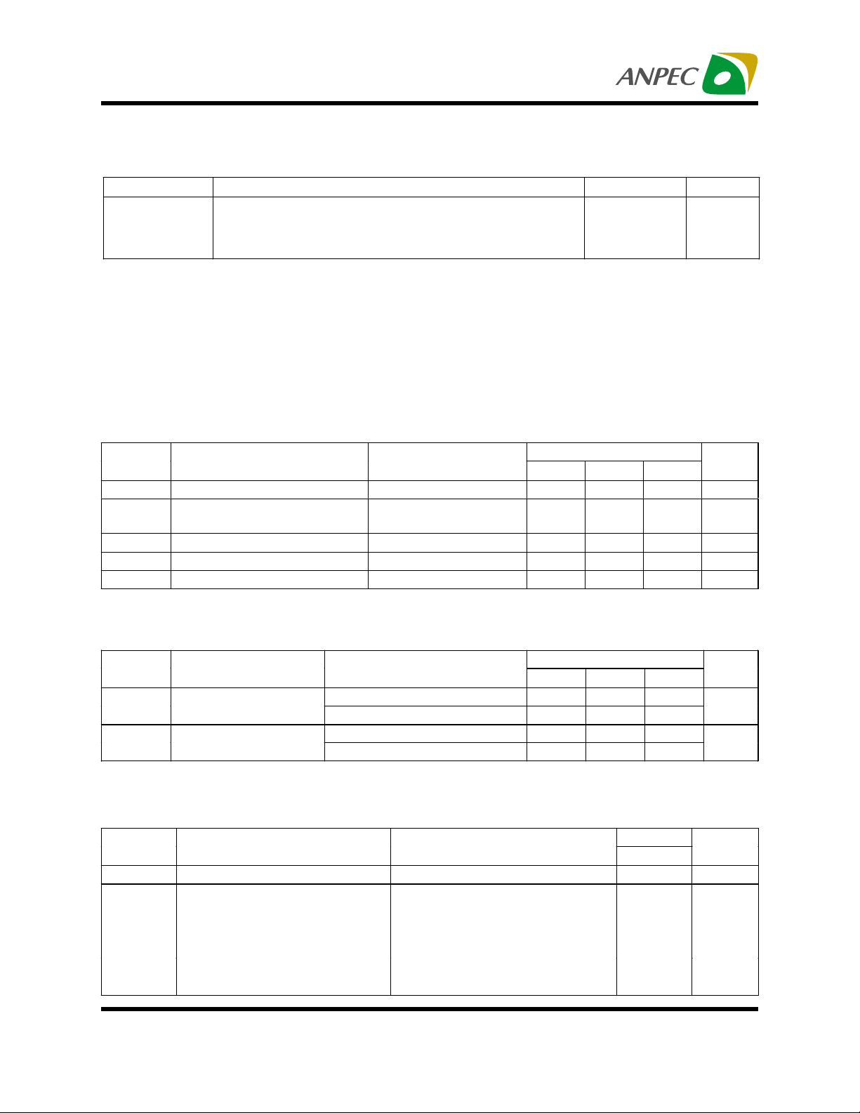
Absolute Maximum Ratings
(Over operating free-air temperature range unless otherwise noted.)
Symbol Parameter Rating Unit
V
DD
T
A
T
J
T
STG
T
S
V
ESD
Note :*1. APA4835 integrates internal thermal shutdown protection when junction temperature ramp up to 150°C.
*2. Human body model : C=100pF, R=1500Ω, 3 positive pulses plus 3 negative pulses
Copyright ANPEC Electronics Corp.
Rev. A.7 - Mar., 2003
Supply Voltage 6 V
Operating Ambient Temperature Range -40 to 85
Maximum Junction Temperature Internally limited*
1
Storage Temperature Range -65 to +150
Soldering Temperature,10 seconds 260
Electrostatic Discharge -2000 to 2000*
2
www.anpec.com.tw2
C
°
C
°
C
°
C
°
V
Page 3
APA4835
Thermal Characteristics
Symbol
R
THJA
*5in2 printed circuit board with 2oz trace and copper pad through 12 25mil diameter vias. The thermal pad on the TSSOP_P package
without solder on the printed circuit board.
**5in2 printed circuit board with 2oz trace and copper pad through 12 25mil diameter vias. The thermal pad on the TSSOP_P package
with solder on the printed circuit board.
Thermal Resistance from Junction to Ambient in Free Air
Parameter Rating Unit
TSSOP-P*
TSSOP-P**
60
35
°C/W
Electical Characteristics
Electrical Characteristics for Entire IC
The following specifications apply for VDD= 5V unless otherwise noted. Limits apply for TA= 25°C
APA4835Symbol Parameter Test Conditions
Min. Typ. Max.
V
I
Supply Voltage 3.3 5.5 V
DD
Quiescent Power Supply
DD
VIN=0V, IO=0A 13 25 mA
Current
I
V
V
Shutdown Current V
SD
SE/BTL High Input Voltage 4 V
IH
SE/BTL Low In put Voltage 0.8 V
IL
PIN 2
= V
DD
0.7 2.0
Unit
A
µ
Electrical Characteristics for Volume Attenuators
The following specifications apply for VDD= 5V. Limits apply for TA= 25°C
Min. Typ. Max.
RANGE
M
Attenuator Range
Mute Attenuation
Gain with V
Attenuation with V
V
=5V, Bridged Mode -88A
PIN 5
=5V, Single-Ended Mode -88
V
PIN 5
PIN 7
=5V ±0.5C
=0V -90 -105
PIN 7
Electrical Characteristics for BTL Mode Operation
The following specifications apply for VDD= 5V unless otherwise noted. Limits apply for TA= 25°C
V
P
Output Offset Voltage VIN=0V 5 mV
OS
O
Output Power
THD=1%, f=1kHz
R
=3
Ω
L
R
=4
Ω
L
R
=8
Ω
L
THD=10%, f=1kHz
=8
R
Ω
L
Copyright ANPEC Electronics Corp.
Rev. A.7 - Mar., 2003
APA4835Symbol Parameter Test Conditions
Unit
dB
dB
APA4835 UnitSymbol Parameter Test Conditions
Typ.
2.2
W
2.0
1.2
1.5
www.anpec.com.tw3
Page 4
APA4835
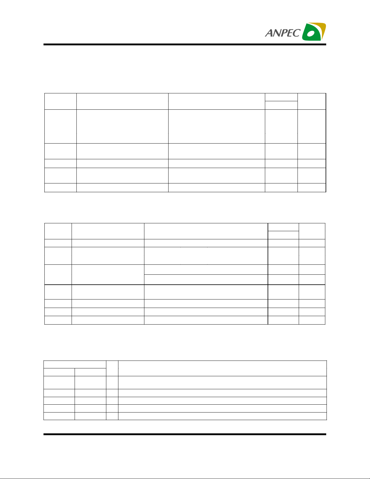
Electical Characteristics (Cont.)
Electrical Characteristics for BTL Mode Operation (Cont.)
The following specifications apply for VDD= 5V unless otherwise noted. Limits apply for TA= 25°C
THD+N Total Harmonic Distortion + Noise
PSRR Power Supply Rejection Ratio
X
TALK
Channel Separation
SNR Signal-to-Noise Ratio
V
Output Noise Voltage
N
Electrical Characteristics for SE Mode Operation
The following specifications apply for VDD= 5V unless otherwise noted. Limits apply for TA= 25°C
AVD=2, 20Hz<f<20kHz
R
=4Ω , PO =1W
L
R
=8Ω , PO=1W
L
=32Ω , PO =340mW
R
L
V
=200mV
RIPPLE
C
=2.2µF, f=120Hz
B
f=1kHz , C
V
=5V, PO =1.1W, RL=8Ω,A-Wtd
DD
B
Rms
=2.2µF
, RL=8
Ω
Filter
R
=8Ω,A-Wtd Filter
L
APA4835 UnitSymbol Parameter Test Conditions
Typ.
0.2
0.15
0.1
74 dB
95 dB
95 dB
30 uV
%
APA4835Symbol Parameter Test Conditions
Unit
Typ.
V
THD+N
PSRR Power Supply Rejectio n
Output Offset Voltage VIN=0V 5 mV
OS
P
Output Power
O
Total Harmonic Distortion
plus Noise
THD=1%, f=1kHz,
THD=10%, f=1kHz,
AV= 1 , V
=75mW, RL=32Ω, AV= 1, f=1kHz
P
O
V
RIPPLE
=1V
OUT
=200mV
RMS
RMS
R
=32
L
R
=32
L
, f=1kHz, RL=1k
, f=120Hz, CB=2.2µF
Ω
Ω
Ω
0.005 %
95
100
mW
0.01 %
58 dB
Ratio
X
SNR Signal-to-Noise Ratio
Channel Separation
TALK
V
Output Noise Voltage
N
f=1kHz , C
P
=75mW, RL=32Ω, A-Wtd Filter
O
=1kΩ, A-Wtd Filter
R
L
=2.2µF
B
95 dB
102 dB
40 uV
Pin Description
Pin
Name No
GND 1, 8, 14, 20,
23
Shutdown 2 I Shutdown mode control signal input, place entire IC in shutdown mode when held high, Idd=0.7u A
Gain Select 3 I Gain select input pin
Mode 4 I Mode select input pin
Mute 5 I Mute control input pin
I/O Description
Ground connection for circuitry.
Copyright ANPEC Electronics Corp.
Rev. A.7 - Mar., 2003
www.anpec.com.tw4
Page 5
APA4835
Pin Description
Pin
Name No
VDD 6, 16, 27 Supply voltage input pin
DC_Vol 7 I Volume control function input pin.
Right Dock 9 O Right docking out put pin
Right In 10 I Right channel audio input pin
Beep In 11 I Beep signal input pin
Left In 12 I Left channel audio input pin
Left Doc k 13 O Right docking output pin
Left Out + 15 O Left channel positive output pin
Left Out - 17 O Left channel negative output pin
Left Gain 2 18 Connect pin 2 of the external gain setting resistor for left channel
Left Gain 1 19 Connect pin 1 of the external gain setting resistor for left channel
HP Sense 21 I Headphone sense control pin
Bypass 22 Bypass pin
Right Gain 1 24 Connect pin 1 of the external gain setting resistor for right channel
Right Gain 2 25 Connect pin 2 of the external gain setting resistor for right channel
Right Ou t - 26 O Right channel negative output pi n
Right Ou t + 28 O Right channel po sitive out put pin
I/O Description
Truth Table for Logic Inputs
Mute Mode HP Sense DC Vol. Control Bridged Output
0 0 0 Fixed Level V ol. Fixed 0 0 1 Fixed Level Muted Vol. Fi xed
0 1 0 Adjusted Vol. Changes 0 1 1 Adjusted Muted Vol. Changed
1××-MutedMuted
Copyright ANPEC Electronics Corp.
Rev. A.7 - Mar., 2003
Single-Ended
www.anpec.com.tw5
Page 6
APA4835
Typical Application Circuit
To Control Pin on
Headphone Jack
Beep In
Right
Audio
Inpu t
20K
200KΩ
200KΩ
20KΩ
100K
Ω
V
DD
Ω
Left Dock
Left In
0.33
Righ t In
0.33
Right Dock
V
DD
1,8,14,20,23
GND
µF0.1µF0.1µF
0.1
100K
Mute
Mode
20K
+
µF
+
µF
20K
6,16,27
Bypass
HP Sense
Ω
21
5
4
13
Ω
12
11
10
Ω
9
22
2.2µF
R_var
Intern a l g a in select
Mode
Control
Beep
Detect
Power
Management
Click and Pop
Suppression
Circuitry
V
DD
r*=R_var/50
+
Bias
+
-
1 µF
V
DD
73
Volume
Control
32 steps
DC Vol Control
20K
19
10K
10KΩ
18
10K
20K
20KΩ20KΩ
10KΩ
25242
+
+
-
20KΩ
Ω
Ω20KΩ
17
15
28
26
Ω
20K
- Left Out
+
220µ F
+ Le ft O ut
+ Right Out
- Right Out
+
220µ F
20KΩ
0.068µ F
0.068µF
Ω
1K
To HP sense
Circuit
Control
Pin
Headphone Jack
1KΩ
Ring
Tip
Pin
Sleeve
Ω
Ω
+
+
-
Shutdown
20K
Ω20KΩ
* Add a resistor to avoid volume control gain error at power on status. For the R_var with 10KΩ variable resistor, the recommended
value of r is in range of 100~200Ω.
Copyright ANPEC Electronics Corp.
Rev. A.7 - Mar., 2003
www.anpec.com.tw6
Page 7
APA4835
Typical Characteristics
10
VDD=5V
5
RL=3Ω
Po=1.75W
2
1
0.5
0.2
0.1
0.05
0.02
0.01
BTL
20 20k50 100 200 500 1k 2k 5k 10k
THD+N-Total Harmonic Distortion+Noise (%)
10
VDD=5V
5
RL=8Ω
Po=1.0W
2
1
0.5
BTL
10
VDD=5V
5
RL=4Ω
Po=1.5W
2
BTL
1
0.5
0.2
0.1
0.05
0.02
0.01
20 20k50 100 200 500 1k 2k 5k 10k
THD+N-Total Harmonic Distortion+Noise (%)
Frequency (Hz)Frequency (Hz)
VDD=5V
5
RL=16Ω
Po=0.5W
2
1
0.5
BTL
0.2
0.1
0.05
0.02
0.01
20 20k50 100 200 500 1k 2k 5k 10k
AV=2AV=8
AV=4
THD+N-Total Harmonic Distortion+Noise (%)
Copyright ANPEC Electronics Corp.
Rev. A.7 - Mar., 2003
0.2
0.1
0.05
0.02
0.01
20 20k50 100 200 500 1k 2k 5k 10k
AV=4
AV=2
AV=8
THD+N-Total Harmonic Distortion+Noise (%)
Frequency (Hz)Frequency (Hz)
www.anpec.com.tw7
Page 8

APA4835
Typical Characteristics Cont.
10
VDD=5V
5
RL=3Ω
2
1
0.5
0.2
0.1
0.05
0.02
0.01
10m 320m 50m 100m 200m 500m 1 2
BTL
f=20kHz
f=1kHz
f=20Hz
THD+N-Total Harmonic Distortion+Noise (%)
10
VDD=5V
5
RL=8Ω
2
1
0.5
0.2
0.1
0.05
0.02
0.01
10m 220m 50m 100m 200m 500m 1
BTL
f=20kHz
f=1kHz
f=20Hz
10
VDD=5V
5
RL=4Ω
2
1
0.5
0.2
0.1
0.05
0.02
0.01
100m 3200m 300m 500m 800m 1 2
BTL
f=20kHz
f=1kHz
f=20Hz
THD+N-Total Harmonic Distortion+Noise (%)
Output Power (W)Output Power (W)
10
VDD=5V
5
RL=16Ω
2
1
0.5
0.2
0.1
0.05
0.02
0.01
10m 120m 50m 100m 200m 500m
BTL
f=20kHz
f=1kHz
f=20Hz
THD+N-Total Harmonic Distortion+Noise (%)
Copyright ANPEC Electronics Corp.
Rev. A.7 - Mar., 2003
THD+N-Total Harmonic Distortion+Noise (%)
Output Power (W)Output Power (W)
www.anpec.com.tw8
Page 9

APA4835
Typical Characteristics Cont.
10
VDD=5V
5
RL=8Ω
Po=0.25W
2
1
0.5
0.2
0.1
0.05
0.02
0.01
SE
AV=1
AV=4
AV=2
20 20k50 100 200 500 1k 2k 5k 10k
THD+N-Total Harmonic Distortion+Noise (%)
10
VDD=5V
5
RL=10kΩ
2
Vin=1Vrms
1
0.5
0.1
0.05
0.02
0.01
0.005
0.002
0.001
SE
AV=1
AV=4
AV=2
20 20k50 100 200 500 1k 2k 5k 10k
10
VDD=5V
5
RL=32Ω
2
Po=75mW
1
0.5
0.1
0.05
0.02
0.01
0.005
0.002
0.001
SE
AV=1
AV=4
AV=2
20 20k50 100 200 500 1k 2k 5k 10k
THD+N-Total Harmonic Distortion+Noise (%)
Frequency (Hz)Frequency (Hz)
10
VDD=5V
5
RL=8Ω
2
1
0.5
0.2
0.1
0.05
0.02
0.01
10m 500m20m 30m 50m 70m 200m
SE
f=20kHz
f=20Hz
f=1kHz
THD+N-Total Harmonic Distortion+Noise (%)
Copyright ANPEC Electronics Corp.
Rev. A.7 - Mar., 2003
THD+N-Total Harmonic Distortion+Noise (%)
Output Power (W)Froquency (Hz)
www.anpec.com.tw9
Page 10

APA4835
Typical Characteristics Cont.
10
VDD=5V
5
RL=32Ω
2
1
0.5
0.1
0.05
0.02
0.01
0.005
0.002
0.001
10m 200m20m 30m 50m 70m 100m
SE
f=20kHz
f=20Hz
f=1kHz
THD+N-Total Harmonic Distortion+Noise (%)
10
VDD=3.3V
5
RL=4Ω
Po=0.65W
2
1
0.5
0.2
0.1
0.05
0.02
0.01
BTL
AV=8
AV=2
AV=4
20 20k50 100 200 500 1k 2k 5k 10k
10
VDD=5V
5
RL=10kΩ
2
1
0.5
0.1
0.05
0.02
0.01
0.005
0.002
0.001
100m 3200m 300m 500m 800m1 2
SE
f=20kHz
f=1kHz
f=20Hz
THD+N-Total Harmonic Distortion+Noise (%)
Output Voltage (V)Output Power (W))
10
VDD=3.3V
5
RL=8Ω
Po=0.4W
2
1
0.5
0.2
0.1
0.05
0.02
0.01
BTL
AV=2
AV=8
AV=4
20 20k50 100 200 500 1k 2k 5k 10k
THD+N-Total Harmonic Distortion+Noise (%)
Copyright ANPEC Electronics Corp.
Rev. A.7 - Mar., 2003
THD+N-Total Harmonic Distortion+Noise (%)
Frequency (Hz)Frequency (Hz)
www.anpec.com.tw10
Page 11

APA4835
Typical Characteristics Cont.
10
VDD=3.3V
5
RL=16Ω
Po=0.2W
2
1
0.5
0.2
0.1
0.05
0.02
0.01
BTL
AV=2
AV=8
AV=4
20 20k50 100 200 500 1k 2k 5k 10k
THD+N-Total Harmonic Distortion+Noise (%)
10
VDD=3.3V
5
RL=8Ω
2
1
0.5
BTL
f=20kHz
10
VDD=3.3V
5
RL=4Ω
2
1
0.5
0.2
0.1
0.05
0.02
0.01
10m 120m 50m 100m 200m 500m
BTL
f=20kHz
f=1kHz
f=20Hz
THD+N-Total Harmonic Distortion+Noise (%)
Output Power (W)Output Power (W)
10
VDD=3.3V
5
RL=16Ω
BTL
2
1
0.5
f=20kHz
0.2
0.1
0.05
0.02
0.01
10m 800m20m 30m 50m 80m 200m 400m
f=1kHz
f=20Hz
THD+N-Total Harmonic Distortion+Noise (%)
Copyright ANPEC Electronics Corp.
Rev. A.7 - Mar., 2003
0.2
0.1
0.05
f=1kHz
f=20Hz
0.02
0.01
10m 500m20m 30m 50m 70m 200m
THD+N-Total Harmonic Distortion+Noise (%)
Output Power (W)Output Power (W)
www.anpec.com.tw11
Page 12

APA4835
Typical Characteristics Cont.
10
VDD=3.3V
5
RL=8Ω
Po=100mW
2
1
0.5
0.2
0.1
0.05
0.02
0.01
SE
AV=1
AV=4
AV=2
20 20k50 100 200 500 1k 2k 5k 10k
THD+N-Total Harmonic Distortion+Noise (%)
10
VDD=3.3V
5
RL=10kΩ
Vin=1Vp
2
1
0.5
SE
10
VDD=3.3V
5
RL=32Ω
Po=35mW
2
1
0.5
0.2
0.1
0.05
0.02
0.01
SE
AV=1
AV=4
AV=2
20 20k50 100 200 500 1k 2k 5k 10k
THD+N-Total Harmonic Distortion+Noise (%)
Frequency (Hz)Frequency (Hz)
10
VDD=3.3V
5
RL=8Ω
2
1
0.5
SE
f=20kHz
0.2
0.1
0.05
0.02
AV=1
AV=2
AV=4
0.01
20 20k50 100 200 500 1k 2k 5k 10k
THD+N-Total Harmonic Distortion+Noise (%)
Copyright ANPEC Electronics Corp.
Rev. A.7 - Mar., 2003
0.2
0.1
0.05
f=20Hz
f=1kHz
0.02
0.01
10m 200m20m 30m 50m 70m 100m
THD+N-Total Harmonic Distortion+Noise (%)
Output Power (W)Frequency (Hz)
www.anpec.com.tw12
Page 13

APA4835
Typical Characteristics Cont.
10
VDD=3.3V
5
RL=32Ω
2
1
0.5
0.2
0.1
0.05
SE
f=20kHz
f=1kHz
0.02
0.01
10m 55m12m 15m 20m 25m 30m 35m 42m
f=20Hz
THD+N-Total Harmonic Distortion+Noise (%)
10
VDD=5V
5
RL=10kΩ
2
docking
1
0.5
0.1
0.05
0.02
0.01
0.005
0.002
0.001
100m 3200m 300m 500m 800m1 2
f=20kHz
f=1kHz
f=20Hz
10
VDD=3.3V
5
RL=10kΩ
2
1
0.5
0.2
0.1
0.05
0.02
0.01
100m 2200m 300m 500m 700m 1
SE
f=1kHz
f=20kHz
f=20Hz
THD+N-Total Harmonic Distortion+Noise (%)THD+N-Total Harmonic Distortion+Noise (%)
Output Voltage (V)Output Power (W)
10
VDD=3.3V
5
RL=10kΩ
docking
2
1
0.5
0.2
0.1
0.05
0.02
0.006
100m 2200m 300m 500m 700m 1
f=20kHz
f=1kHz
f=20Hz
THD+N-Total Harmonic Distortion+Noise (%)
Output Voltage (V) Output Voltage (V)
Copyright ANPEC Electronics Corp.
Rev. A.7 - Mar., 2003
www.anpec.com.tw13
Page 14

APA4835
Typical Characteristics Cont.
100u
50u
20u
10u
5u
No filter
A_wtd filter
VDD=5V
-Output Noise Voltage( V)
N
V
RL=8Ω
2u
Av=2V/V
BTL
1u
20 20k50 100 200 500 1k 2k 5k 10k
Frequency (Hz) Frequency (Hz)
+0
VDD=5V
RL=8Ω
-20
Po=1W
Av=2V/V
-40
BTL
100u
No filter
50u
A_wtd filter
20u
10u
5u
VDD=5V
-Output Noise Voltage( V)
N
2u
RL=10kΩ
Av=1V/V
SE
1u
20 20k50 100 200 500 1k 2k 5k 10k
+0
VDD=5V
RL=32Ω
-20
Po=75mW
Av=1V/V
-40
SE
-60
-80
Crosstalk (dB)
-100
f=20kHz
-120
20 20k50 100 200 500 1k 2k 5k 10k
Frequency (Hz) Frequency (Hz)
Copyright ANPEC Electronics Corp.
Rev. A.7 - Mar., 2003
f=1kHz
-60
-80
Crosstalk (dB) V
f=1kHz
-100
f=20kHz
-120
20 20k50 100 200 500 1k 2k 5k 10k
www.anpec.com.tw14
Page 15

APA4835
4
Typical Characteristics Cont.
+12
+10
+8
Cf=0.068µF
+6
Gain (dBV)
+4
Cf=0.22µF
Cf=0.1µF
VDD=5V
+2
-0
20 20k50 100 200 500 1k 2k 5k 10k
Av=2V/V
Frequency (Hz)
0.7
0.6
0.5
0.4
RL=16Ω
0.3
0.2
0.1
-Power Disspation (W)
D
P
0
0 0.25 0.5 0.75 1 1.25 1.5
RL=32Ω
RL=8Ω
VDD=5V
THD<1%
RL=8Ω
BTL
BTL
2
1.8
1.6
1.4
1.2
1
0.8
0.6
-Power Disspation (W)P
D
0.4
P
0.2
0
0 0.5 1 1.5 2 2.5
RL=3Ω
RL=4Ω
VDD=5V
THD<1%
Output Power (W)
0.2
0.18
0.16
0.14
0.12
0.1
0.08
0.06
0.04
-Power Disspation (W)
D
0.02
0
0 0.05 0.1 0.15 0.2 0.25 0.3 0.35 0.
RL=16Ω
RL=32Ω
RL=8Ω
VDD=5V
THD<1%
BTL
SE
Output Power (W)Output Power (W)
Copyright ANPEC Electronics Corp.
Rev. A.7 - Mar., 2003
www.anpec.com.tw15
Page 16

APA4835
Typical Characteristics Cont.
20
No Load
17.5
15
12.5
10
7.5
-Supply Current (mA)
5
DD
I
2.5
0
11.522.533.544.555.5
BTL
SE
VDD-Supply Voltage (V) VDD-Supply Voltage (V)
0.16
0.14
0.12
0.1
VDD=5V
RL=32Ω
SE
2
1.8
1.6
1.4
1.2
0.8
0.6
Output Power (W)Output Power (W)
0.4
0.2
VDD=5V
RL=8Ω
BTL
1
THD=10%
THD=1%
0
2.5 3 3.5 4 4.5 5 5.5
3
VDD=5V
2.5
2
BTL
0.08
THD=10%
0.06
Output Power (W)
0.04
0.02
0
2.5 3 3.5 4 4.5 5 5.5
VDD-Supply Voltage (V)
Copyright ANPEC Electronics Corp.
Rev. A.7 - Mar., 2003
THD=1%
1.5
1
0.5
THD=1%
0
4 8 12 16 20 24 28 32 36 40 44 48 52 56 60 64
THD=10%
Load Resistance (Ω)
www.anpec.com.tw16
Page 17

APA4835
Typical Characteristics Cont.
0.8
VDD=5V
0.7
0.6
0.5
0.4
0.3
Output Power (W)
0.2
THD=1%
0.1
0
4 8 12 16 20 24 28 32 36 40 44 48 52 56 60 64
THD=10%
Load Resistance (Ω) Load Resistance (Ω)
0.34
0.32
0.3
0.28
0.26
0.24
0.22
0.2
0.18
0.16
0.14
0.12
0.1
Output Power (W)
0.08
0.06
0.04
0.02
THD=1%
0
4 8 12 16 20 24 28 32 36 40 44 48 52 56 60 64
THD=10%
VDD=3.3V
SE
SE
1.1
1
0.9
0.8
0.7
0.6
0.5
0.4
0.3
Output Power (W)
0.2
THD=1%
0.1
0
4 8 12 16 20 24 28 32 36 40 44 48 52 56 60 64
20
THD=10%
VDD=3.3V
VDD=5V
0
-20
-40
-60
SE
Gsin (dBV)
-80
-100
-120
0.0 0.5 1.0 1.5 2.0 2.5 3.0 3.5 4.0 4.5 5.0
BTL
Load Resistance (Ω)
Copyright ANPEC Electronics Corp.
Rev. A.7 - Mar., 2003
Voltage (V)
www.anpec.com.tw17
Page 18

APA4835
Typical Characteristics Cont.
+0
VDD=5V
-10
Vin=200mVp
-20
-30
-40
-50
PRSS (dBgA)
-60
-70
-80
RL=8Ω
Cb=2.2µF
SE/BTL
20 20k50 100 200 500 1k 2k 5k
Frequency (Hz)
Copyright ANPEC Electronics Corp.
Rev. A.7 - Mar., 2003
www.anpec.com.tw18
Page 19

APA4835
φ
φ
Packaging Information
TS SOP / T S SO P-P ( Re fe ren c e JE DE C R e g is tratio n MO-15 3 )
e
N
2 x E / 2
E1 E
12
3
e/2
EXPOSED THERMAL
PAD ZONE
D
b
D1
A2
A
A1
E2
0.25
(3)
S
(2)
(L1)
L
GAUGE
PLANE
1
BOTTOM VIEW
Millime te rs Inc h e s
Dim
(THERMALLY ENHANCED VARIATIONDS ONLY)
Min. Max. Min. Max.
A1.20.047
A1 0.00 0.15 0.000 0.006
A2 0.80 1.05 0.031 0.041
b 0.1 9 0.3 0 .0 07 0.0 12
D
D1
6.4 (N=20PIN)
7.7 (N=24PIN)
9.6 (N=28PIN)
4.2 BSC (N=20P IN)
4.7 BSC (N=24P IN)
3.8 BSC (N=28P IN)
6.6 (N=20PIN)
7.9 (N=24PIN)
9.8 (N=28PIN)
0.252 (N=20PIN)
0.303 (N=24PIN)
0.378 (N=28PIN)
0.165 BSC (N=20PIN)
0.188 BSC (N=24PIN)
0.150 BSC (N=28PIN)
0.260 (N=20PIN)
0.311 (N=24PIN)
0.386 (N=28PIN)
e 0.65 BS C 0.026 BS C
E 6.40 B S C 0.252 BS C
E1 4.30 4.50 0.169 0.177
E2 3.0 BSC (N=20PIN)
3.2 BSC (N=24P IN)
2.8 BSC (N=28P IN)
0.118 B S C (N=2 0P IN)
0.127 BSC (N=24PIN)
0.110 B S C (N=2 8P IN)
L 0.4 5 0.7 5 0 .0 18 0.03 0
L1 1.0 REF 0.039RE F
R 0.0 9 0.00 4
R1 0.09 0.004
S0.2 0.008
10°8
212
REF 12° REF
°
°
0
°
8
°
Copyright ANPEC Electronics Corp.
Rev. A.7 - Mar., 2003
www.anpec.com.tw19
Page 20

APA4835
Physical Specifications
Terminal Material Solder-Plated Copper (Solder Material : 90/10 or 63/37 SnPb)
Lead So ld e rability Meets EIA Specification RSI86-91 , A NSI/J-STD-002 Category 3.
Reflow Condition (IR/Convection or VPR Reflow)
Reference JEDEC Standard J-STD-020A APRIL 1999
Peak temperature
temperature
Pre-heat temperature
°
183 C
Classification R e flow Profiles
Convection or IR/
Convection
Average ramp-up rate(183°C to Peak) 3°C/second max. 10 °C /second max.
Preheat temperature 125 ± 25°C)
Temperature maintained above 183°C
Time within 5°C of actual peak temperature
Peak temperature range
Ramp-down rate
Time 25°C to peak temperature
120 seconds max
60 – 150 seconds
10 –20 seconds 60 seconds
220 +5/-0°C or 235 +5/-0°C 215-219°C or 235 +5/-0°C
6 °C /second max. 10 °C /second max.
6 minutes max.
VPR
Time
Package Reflow Conditions
pkg. thickness ≥≥≥≥ 2.5mm
and all bgas
Convection 220 +5/-0 °C Convection 235 +5/-0 °C
VPR 215-219 °C VPR 235 +5/-0 °C
IR/Convection 220 +5/-0 °C IR/Convection 235 +5/-0 °C
Copyright ANPEC Electronics Corp.
Rev. A.7 - Mar., 2003
pkg. thickness < 2.5mm and
pkg. volume ≥≥≥≥ 350 mm³
pkg. thickness < 2.5mm and pkg.
volume < 350mm³
www.anpec.com.tw20
Page 21

APA4835
Reliability test pro gram
Test item Method Description
SOLDERABILITY M IL-STD-883D-2003
HOLT MIL-STD-883D-1005.7
PCT JESD-22-B, A102
TST MIL-STD-883D-1011.9
ESD MIL-STD-883D-3015.7 VHBM > 2KV, VMM > 200V
Latch-U p JESD 78 10ms , Itr > 100mA
Carrier Tape & Reel Dimensions
245°C , 5 SEC
1000 Hrs Bias @ 125 °C
168 Hrs, 100 % RH , 121°C
-65°C ~ 150°C, 200 C y c les
t
E
Po
F
W
A
P
P1
Ao
J
D
Bo
Ko
D1
T2
C
B
Copyright ANPEC Electronics Corp.
Rev. A.7 - Mar., 2003
T1
www.anpec.com.tw21
Page 22

APA4835
Applic a tio n
TSSOP- 20
Applic a tio n
TSSOP- 24
Applic a tio n
TSSOP- 28
A B C J T1 T2 W P E
330 ±1 100 ref 13 ±0.5 2 ±0.5 16.4 ±0.2 2 ±0.2 16 ±0.3 8.0 ±0.1 1.75±0.1
F D D1 Po P1 Ao Bo Ko t
7.5 ±0 .1 1.5 + 0 .1 1 .5 m in 4 .0 ±0.1 2.0 ±0.1 6.8 ±0.1 6.9 ±0.1 1.6 ±0.1 0.3±0.05
A B C J T1 T2 W P E
330 ±1 100 ref 13 ±0.5 2 ±0.5 16.4 ±0.2 2 ±0.2 16 ±0.3 12 ±0.1 1.75±0.1
F D D1 Po P1 Ao Bo Ko t
7.5 ±0 .1 1.5 + 0 .1 1 .5 m in 4 .0 ±0.1 2.0 ±0.1 6.9 ±0.1 8.3 ±0.1 1.5 ±0.1 0.3±0.05
A B C J T1 T2 W P E
330 ±1 100 ref 13 ±0.5 2 ±0.5 16.4 ±0.2 2 ±0.2 16 ±0.3 12 ±0.1 1.75±0.1
F D D1 Po P1 Ao Bo Ko t
7.5 ±0 .1 1.5 + 0 .1 1 .5 m in 4 .0 ±0.1 2.0 ±0.1 6.9 ±0.1 10.2 ±0.1 1.8 ±0.1 0.3±0.05
(mm)
Cover Tape Dimensions
Application Carrier Width Cover Tape Width Devices Per Reel
TSSOP- 20 / 24 / 28
16 21.3 2000
Customer Service
Anpec Electronics Corp.
Head Office :
5F, No. 2 Li-Hsin Road, SBIP,
Hsin-Chu, Taiwan, R.O.C.
Tel : 886-3-5642000
Fax : 886-3-5642050
Taipei Branch :
7F, No. 137, Lane 235, Pac Chiao Rd.,
Hsin Tien City, Taipei Hsien, Taiwan, R. O. C.
Tel : 886-2-89191368
Fax : 886-2-89191369
Copyright ANPEC Electronics Corp.
Rev. A.7 - Mar., 2003
www.anpec.com.tw22
 Loading...