

Datasheet APA3544KI-TU, APA3544KI-TR, APA3544JI-TU, APA3544JI-TR, APA3541KI-TU Datasheet (ANPEC)
...Page 1
APA3541/4
Class AB Stereo Headphone Driver with Mute
Features
••
• High Signal-to-Noise Ratio
••
••
• High Slew Rate
••
••
• Low Distortion
••
••
• Large Output Voltage Swing
••
••
• Flexible Mute Function
••
••
• Excellent Power Supply Ripple Rejection
••
••
• Low Power Consumption
••
••
• Short-circuit Elimination
••
••
• Wide Temperature Range
••
••
• No Switch ON/OFF Clicks
••
••
• Integrated Voltage Divider (V
••
External Resistors
/2) to Eliminate
DD
Applications
••
• Portable Digital Audio
••
General Description
The APA3541/4 is an integrated class AB stereo
headphone driver contained in an SO-8 or a DIP-8
plastic package with Mute feature . Besides the common Mute feature , the APA3541/4 further integrates
a voltage divider inside the chip . Thus , the external
resistors can be eliminated . The APA3541 has a fixed
gain of 0dB and the APA3544 has a fixed gain of 6dB
so that external gain setting is unnecessary. The device is fabricated in a CMOS process and has been
primarily developed for portable digital audio applications .
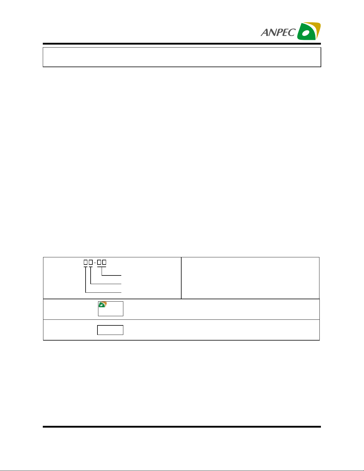
Ordering and Marking Information
APA3541/4
Handling Code
Temp. Range
Package Code
APA3541/4 J : APA3541/4
APA3541/4 K :
ANPEC reserves the right to make changes to improve reliability or manufacturability without notice, and advise
customers to obtain the latest version of relevant information to verify before placing orders.
Copyright ANPEC Electronics Corp.
Rev. B.1 - Apr., 2003
XXXXX
APA3541/4
XXXXX
Package Code
J : P D IP - 8 K : S O P - 8
Y : C h ip F ro m
Temp. Range
I : - 40 to 8 5 C
Handling Code
TU : Tube TR : Tape & Reel
XXXXX - Date Code
XXXXX - Date Code
°
www.anpec.com.tw1
Page 2
APA3541/4
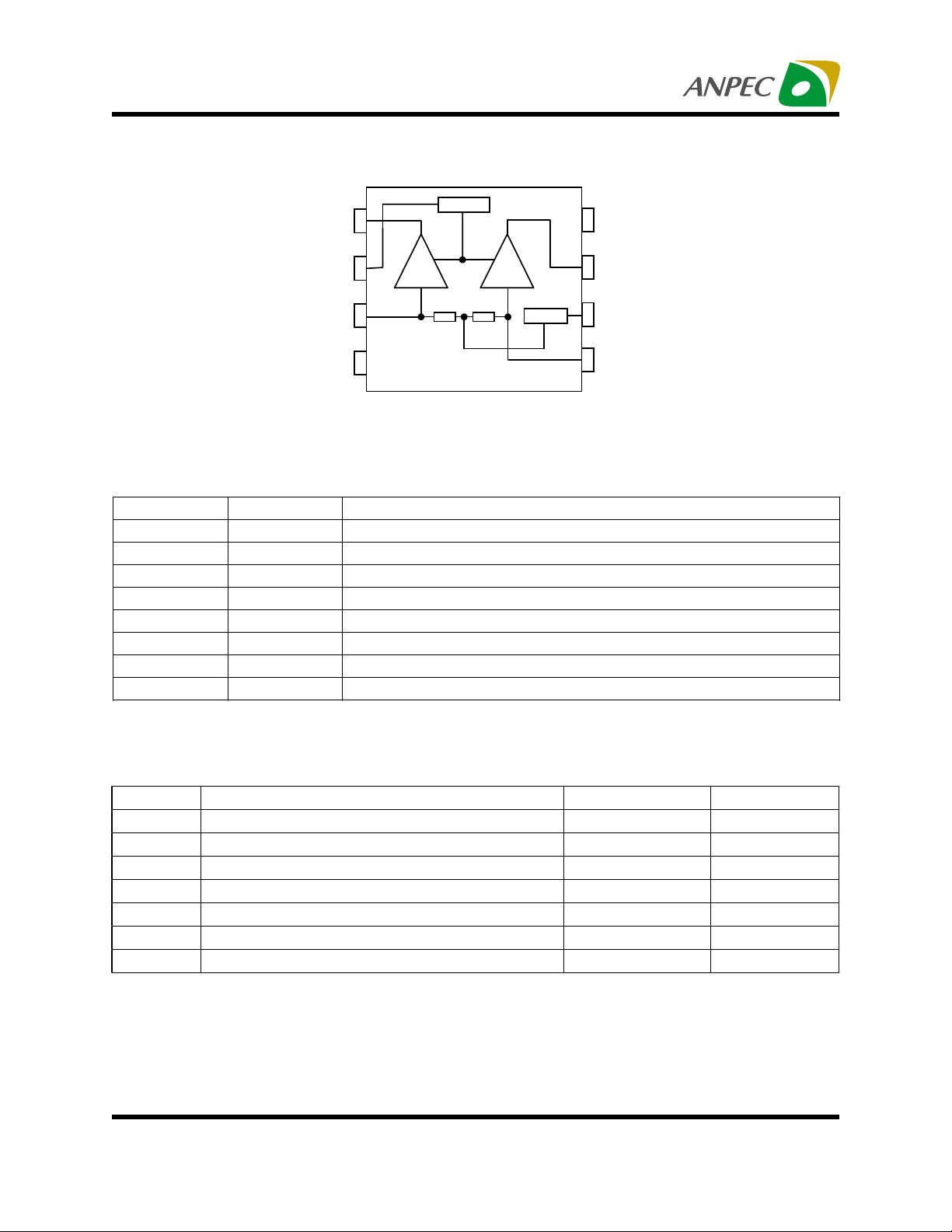
Block Diagram
Out A
Mute
Input A
V
MUTE
1
0dB
(6dB)
2
3
4
SS
* The values in parenthessis are for the APA3544.
A
+
180k
90k
(
Ω)
180k
Ω
90k
(
Ω)
0dB
(6dB)
B
+
BIAS
Ω
8
7
6
5
V
DD
Out B
BIAS
Input B
Function Pin Description
Pin Name I/O Function Description
Out A O A channel output pin
Mute I Chip disable control input, low active and high for normal operating
Input A I A channel input terminal
V
SS
Input B I B channel input terminal
BIAS I Right channel bias input pin
OUT B O B channel output pin
V
DD
Power ground pin
Power input pin
Absolute Maximum Ratings
Symbol Parameter Rating Unit
V
DD
t
SC(O)
T
T
T
STG
T
V
ESD
Note: 1. Human body model : C=100pF, R=1500Ω, 3 positive pulses plus 3 negative pulses
Copyright ANPEC Electronics Corp.
Rev. B.1 -Apr., 2003
Supply Voltage 7 V
Output Short-circuit Duration, at TA=25°C, P
Operating Ambient Temperature range -40 to 85
A
Maximum Junction Temperature 150
J
tot
=1W
20 S
Storage Temperature Range -65 to +150
Soldering Temperature,10 seconds 300
S
Electrostatic Discharge -3000 to 3000
*1
www.anpec.com.tw2
C
°
C
°
C
°
C
°
V
Page 3
APA3541/4
Thermal Characteristics
Symbol Parameter Rating Unit
R
THJA
R
THJC
Electrical Characteristics
VIN=0dBV, VCC=5V, TA=25°C, f=1kHz, RL=32Ω (unless otherwise noted)
Thermal Resistance from Junction to Ambient in Free Air
DIP-8
SOP-8
Thermal Resistance from Junction to Case
DIP-8
SOP-8
108
210
45
40
K/W
K/W
Symbol Parameter Test Condition
V
DD
Supply Voltage 3.0 5.0 6.0 V
I
Q
Quiescent Current VIN= 0 Vrms 3.5 5 mA
Imute
V
G
∆
G
Mute Current 200
Mute Terminal Voltage 0.3 0.7 1.6 V
TM
Differential Channel
VCL
Voltage Gain
VCL
Vin=1Vrms,f= 1kHz,RL=32
Voltage Gain
Ω
Vin=0.5Vrms, f=1kHz,Rl=32
THD
P
P
Total Harmonic Channel
Distortion Factor
U1
Rated Output Power1
U2
Rated Output Power2
BW<80k Hz 0.03 0.1 %
RL=32Ω,THD+N=0.1% ,BW<8
0kHz
RL=16Ω,THD+N=0.1% ,BW<8
0kHz
APM3541/4
Min. Typ. Max.
-0.5 0 0.5 dB
APA3541 -2 0 2
APA3544 4 6 8
Ω
APA3541 50 55
APA3544 75 80
APA3541 105 110
APA3544 140 145
Unit
A
µ
dB
mW
mW
V
NO
Output Noise Voltage BW=20~20kHz , Vin=0Vrms -93 -85 dBV
CS
ATT
RR
Copyright ANPEC Electronics Corp.
Rev. B.1 -Apr., 2003
Channel Separation F=1kHz
Mute Attenuation VIN=1Vrms,f=1kHz,Mute=L 65 70 dB
Ripple Rejection F
APA3541 -90 -95
APA3544 -65 -70
=100Hz,VRR=-20dB V 50 60 dB
RR
www.anpec.com.tw3
dB
Page 4
APA3541/4
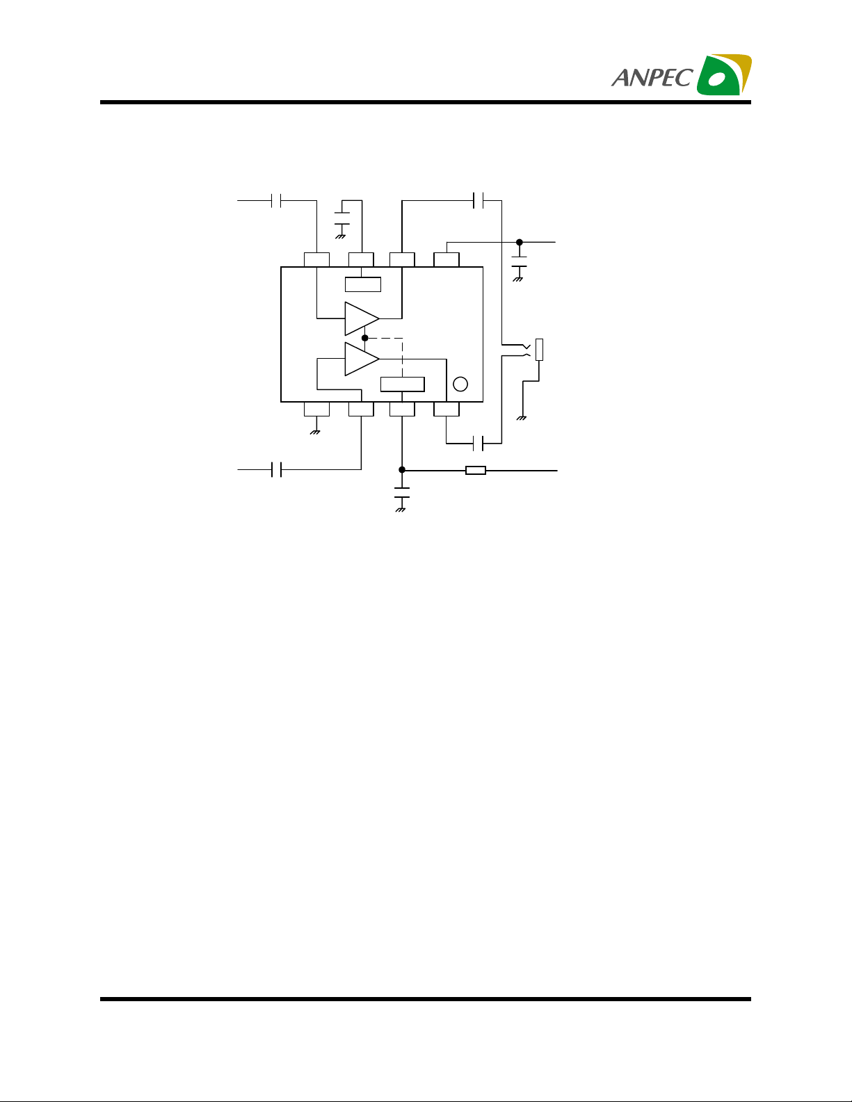
Test and Application Circuit
µ
F
1
V
INB
10µ
F
57
4
V
SS
µ
1
F
V
INA
68
BIAS
0dB(6dB)
+
B
0dB(6dB)
+
A
32 1
Input A
Mute
µ
1
Out BInput B
BIAS
V
(APA3544)
MUTE
Out A
F
DD
APA3541
220µF
220µF
100k
V
DD
100µF
Ω
V
MUTE
H : Speaker Action
L : Mute on
Copyright ANPEC Electronics Corp.
Rev. B.1 -Apr., 2003
www.anpec.com.tw4
Page 5

APA3541/4
Typical Characteristics
8
ΩΩ
RL=32
Ω
7
6
(mA)
Q
5
4
3
2
Quiescent Current : I
1
0
ΩΩ
MUTE : OFF
MUTE : ON
02467531
Figure 1 : Supply Voltage : V
10
0
-10
VDD=5V
(dBV)
OUT
Output Voltage : V
VIN=0dBv
-20
f =1 kHz
-30
ΩΩ
RL=32
Ω
-40
-50
-60
-70
-80
0 0.4 0.8 1.2 1.6 2
ΩΩ
DD
(V)
5
ΩΩ
RL=32
Ω
ΩΩ
4
(V)
bias
3
2
1
Bias DC Voltage :V
0
02467135
Figure 2 : Supply Voltage : V
+8
APA3541
+6
VDD=5V
+4
VIN=0dBv
+2
(dB)
VC
+0
-2
-4
-6
-8
Voltage Gain : G
-10
-12
10 100k100 1k 10k
DD
(V)
Figure 3 : Mute Control Voltage : VTM (V)
Copyright ANPEC Electronics Corp.
Rev. B.1 -Apr., 2003
Figure 4 : Frequency :f (Hz)
www.anpec.com.tw5
Page 6

APA3541/4
Typical Characteristics Cont.
10
5
VDD= 5V
ΩΩ
R
=32
Ω
ΩΩ
L
2
BW< 80kHz
1
0.5
(%)
0.2
f =10kHz
0.1
0.05
f =1kHz , 100Hz
0.02
Total Harmonic Distortion : THD+N
0.01
-40 +10-30 -20 -10 +0
Figure 5 : Output Voltage : V
OUT
(dBv)
10
5
2
1
0.5
0.2
(%)
0.1
0.05
0.02
0.01
Total Harmonic Distortion : THD+N
-40 +10-30 -20 -10 +0
Figure 6 :
VDD= 3V
ΩΩ
RL=32
Ω
ΩΩ
BW< 80kHz
f =10KHz
f =1KHz , 100Hz
Output Voltage : V
OUT
(dBv)
10
5
VDD= 5V
ΩΩ
RL=16
Ω
2
1
0.5
0.2
0.1
0.05
0.02
0.01
Total Harmonic Distortion : THD+N (%)
-40 +10-30 -20 -10 +0
Figure 7 : Output Voltage : V
ΩΩ
BW< 80kHz
f =10kHz
f =1kHz , 100Hz
OUT
(dBv)
10
5
2
1
0.5
0.2
0.1
0.05
0.02
0.01
Total Harmonic Distortion : THD+N (%)
Figure 8 : Output Voltage : V
VDD= 3V
ΩΩ
RL=16
Ω
ΩΩ
BW< 80kHz
f =10kHz
f =1kHz , 100Hz
-40 +10-30 -20 -10 +0
(dBv)
OUT
Copyright ANPEC Electronics Corp.
Rev. B.1 -Apr., 2003
www.anpec.com.tw6
Page 7

APA3541/4
Typical Characteristics Cont.
+0
VDD=5V
-20
RL=32
ΩΩ
Ω
ΩΩ
-40
-60
-80
-100
Channel Separation : CS (dB)
-120
Figure 9 : Frequency :f (Hz)
0
-10
fRR=100Hz
-20
VRR=-20dBv
-30
-40
-50
-60
-70
-80
-90
Ripple Rejection : RR (dB)
-100
02467531
+0
-10
-20
-30
VDD=5V
=0dBv
V
IN
R
=32
L
ΩΩ
Ω
ΩΩ
-40
-50
-60
-70
-80
-90
Mute Attenuationt : ATT(dB)
100k10 100 1k 10k
100
10 100k50100 1k 10k
Figure 10 : Frequency :f (Hz)
Figure 11 : Supply Voltage : V
Copyright ANPEC Electronics Corp.
Rev. B.1 -Apr., 2003
DD
(V)
www.anpec.com.tw7
Page 8

APA3541/4
Application Note
Input Capacitor , Ci
In the typical application an input capacitor , Ci , is
required to allow the amplifier to bias the input signal
to the proper DC level for optimum operation . In this
case , the external capacitor Ci and the internal resistance Ri form a high-pass filter with the corner frequency determined in the follow equation:
fc (highpass)= 1/ (2πRiCi) (1)
The value of Ci is important to consider as it directly
affects the low frequency performance of the circuit.
Consider the APA3541 where Ri is 180kΩ and
APA3544 is 90kΩ internal fixed . Equation is
reconfigured as follow:
Ci= 1/(2π*180kΩ*fc) for APA3541
Ci= 1/(2π*90kΩ*fc) for APA3544 (2)
And the ceramic capacitor is recommanded.
Bias Capacitor , Cb
As with any power amplifier , proper supply bypassing is critical for low noise performance and high
power supply rejection . The capacitor location on
both the bypass and power supply pins should be as
close to the device as possible . The effect of a larger
half supply bias capacitor is improved PSRR due to
increased half-supply stability . Typical applications
employ a 5V regulator with 10µF and a 0 . 1µF bias
capacitors which aid in supply filtering .
This does not eliminate the need for bypassing the
supply nodes of the APA3541/4 . The selection of
bias capacitors , especially Cb , is thus dependent
upon desired PSRR requirements , click and pop performance . The capacitor is fed from a 95kΩ source
inside the amplifier . To keep the start-up pop as low
as possible , the relationship shown in equation should
be maintained .
1/(Cb*95kΩ)≤ 1/{Ci*Ri} (3)
As an example , consider a circuit where Cb is
4.7µF, Ci is 1µF and APA3541 Ri is 180kΩ . Inserting
these values into the equation we get 2.24≤ 5.55
which satisfies the rule . Bias capacitor , Cb , values
of 2.2µF to 10µF ceramic or tantalum low-ESR ca-
pacitors are recommended for the best THD and
noise performance .
Output Coupling Capacitor, Cc
In the typical single-supply SE configuration , an output coupling capacitor (Cc) is required to block the
DC bias at the output of the amplifier thus preventing
DC currents in the load . As with the input coupling
capacitor , the output coupling capacitor and impedance of the load form a high-pass filter governed by
equation .
fc(highpass)= 1/(2πR
Cc) (4)
L
For example , a 220µF capacitor with an 32Ω speaker
would attenuate low frequencies below 22Hz . The
main disadvantage , from a performance standpoint
, is the load impedance is typically small , which drives
the low-frequency corner higher degrading the bass
response . Large values of Cc are required to pass
low frequencies into the load .
Optimizing Depop Circuitry
When the amplifier is in mute mode , both of the output stage and input bypass continues to be biased .
And no pop noise will be heard during the transition
out of mute mode .
Power Supply Decoupling, Cs
APA3541/4 is a high-performance CMOS audio amplifier that requires adequate power supply decoupling
to ensure the output total harmonic distortion (THD)
is as low as possible . Power supply decoupling also
prevents the oscillations causing by long lead length
between the amplifier and the speaker . The optimum
decoupling is achieved by using two different type
capacitors that target on different type of noise on
the power supply leads . For higher frequency transients , spikes , or digital hash on the line , a good
low equivalent-series-resistance (ESR) ceramic
capacitor, typically 0.1µF placed as close as possible
to the device VDD lead works best . For filtering lowerfrequency noise signals , a large aluminum electrolytic capacitor of 10µF or greater placed near the audio
power amplifier is recommended .
Copyright ANPEC Electronics Corp.
Rev. B.1 -Apr., 2003
www.anpec.com.tw8
Page 9

APA3541/4
φ
Packaging Information
PDIP-8 pin ( Reference JEDEC Registration MS-001)
D
E1
1
A
L
e2
e 3
A1
e 1
A2
Millimeters InchesDim
Min. Max. Min. Max.
A
A1
A2
D
e1
e2
e3
E
E1
0.38 0.015
2.92 3.68 0.115 0.145
9.02 10.16 0.355 0.400
2.54BSC 0.100BSC
0.36 0.56 0.014 0.022
1.14 1.78 0.045 0.070
7.62 BSC 0.300 BSC
6.10 7.11 0.240 0.280
E3
L
115
2.92 3.81 0.115 0.150
°
5.33 0.210
10.92 0.430
E
1
E3
15
°
Copyright ANPEC Electronics Corp.
Rev. B.1 -Apr., 2003
www.anpec.com.tw9
Page 10

APA3541/4
Packaging Information
SOP-8 pin ( Reference JEDEC Registration MS-012)
HE
0.015X45
e1 e2
D
A1
A
1
L
0.004max.
Dim
A 1.35 1.75 0.053 0.069
A1 0.10 0.25 0. 004 0.010
D 4.80 5.00 0.189 0.197
E 3.80 4.00 0.150 0.157
H 5.80 6.20 0.228 0.244
L 0.40 1.27 0.016 0.050
e1 0.33 0. 51 0.013 0.020
e2 1.27BSC 0.50BSC
18
φ
Millimeters Inches
Min. Max. Min. Max.
°
8
°
Copyright ANPEC Electronics Corp.
Rev. B.1 -Apr., 2003
www.anpec.com.tw10
Page 11

APA3541/4
Physical Specifications
Ter m ina l Mater ial Solder-Plated Copper (Solder Material : 90/10 or 63/37 Sn Pb)
Lead Solderab ility Me ets E IA Specification RSI86-91, ANSI/J-STD-002 Category 3.
Reflow Condition
Reference JEDEC Standard J-STD-020A APRIL 1999
temperature
Pre-heat temperature
(IR/Convection or VPR Reflow)
°
183 C
Peak temperature
Time
Classification Reflow Prof iles
Convection or IR/
Convection
Average ramp-up rate(183°C to Peak) 3°C/second max. 10 °C /second max .
Preheat temperature 125 ± 25°C)
Temperature maintained above 183°C
Time within 5°C of actual peak temperature
Peak temperature range
Ramp-down rate
Time 25°C to peak temperature
120 seconds max
60 – 150 seconds
10 –20 seconds 60 seconds
220 +5/-0°C or 235 +5/-0°C 215-219°C or 235 +5/-0°C
6 °C /second max . 10 °C /second max .
6 minutes max.
VPR
Package Reflow Conditions
pkg. thickness
and all bgas
Convection 220 +5/-0 °C Convection 235 +5/-0 °C
VPR 215-219 °C VPR 235 +5/-0 °C
IR/Convection 220 +5/-0 °C IR/Convection 235 +5/-0 °C
Copyright ANPEC Electronics Corp.
Rev. B.1 -Apr., 2003
2.5mm
≥≥≥≥
pkg. thickness < 2.5mm and
pkg. volume
350 mm³
≥≥≥≥
pkg. thickness < 2.5mm and pkg.
volume < 350mm³
www.anpec.com.tw11
Page 12

APA3541/4
Reliability test Program
Test item Method Description
SOLDERABILITY MIL-STD-883D-2003
HOLT MIL-STD-883D-1005.7
PCT JESD-22-B, A102
TST MIL-STD-883D-1011.9
ESD MIL-STD-883D-3015.7 VHBM > 2KV, VMM > 200V
Latch-Up JESD 78 10ms , Itr > 100mA
Carrier Tape & Reel Dimensions
°
C , 5 SEC
245
1000 Hrs Bias @ 125
168 Hrs, 100 % RH , 121
°
C ~ 150°C, 200 Cycles
-65
t
°
C
°
C
D1
D
Bo
Ko
T2
B
T1
E
F
W
A
Po
P
P1
Ao
J
C
Application
Copyright ANPEC Electronics Corp.
Rev. B.1 -Apr., 2003
A B C
330 ± 162 +1.5
F D
5.5± 1 1.55 +0.1 1.55+ 0.25 4.0 ± 0.1 2.0 ± 0.1 6.4 ± 0.1 5.2± 0. 1 2.1± 0.1 0.3±0.013
12.75+
0.15
D1 Po P1 Ao Bo Ko tSOP- 8
J T1 T2 W P E
2 ± 0.5 12.4 ± 0.2 2 ± 0.2 12± 0. 3 8± 0.1 1.75±0.1
www.anpec.com.tw12
Page 13

APA3541/4
Cover Tape Dimensions
Application Ca rr ier Width Cover Tape Width Devices P er Reel
SOP- 8
Customer Service
Anpec Electronics Corp.
Head Office :
5F, No. 2 Li-Hsin Road, SBIP,
Hsin-Chu, Taiwan, R.O.C.
Tel : 886-3-5642000
Fax : 886-3-5642050
Taipei Branch :
7F, No. 137, Lane 235, Pac Chiao Rd.,
Hsin Tien City, Taipei Hsien, Taiwan, R. O. C.
Tel : 886-2-89191368
Fax : 886-2-89191369
12 9.3 2500
Copyright ANPEC Electronics Corp.
Rev. B.1 -Apr., 2003
www.anpec.com.tw13
 Loading...