

Page 1
AP562
3.3-3.8 GHz WiMAX 8W Power Amplifier
Product Features
• 3.3 – 3.8 GHz
• +39.4 dBm P1dB
• 11.5 dB Gain
• 2.0% EVM @ 30 dBm Pout
• +12 V Supply Voltage
• Lead-free/green/RoHS-compliant
5x6 mm power DFN package
Applications
• WiMAX CPE/BTS
Specifications
Parameter Units Min Typ Max
Operational Bandwidth GHz 3.3 3.8
Test Frequency GHz 3.5
Output Channel Power dBm +30
Power Gain dB 11.5
Input Return Loss dB 15
Output Return Loss dB 6.7
Error Vector Magnitude % 1.9
Operating Current, Icc mA 685
RF Switching Speed ns 50
Collector Efficiency % 11.7
Output P1dB dBm 39.4
Quiescent Current, Icq mA 400
(4)
Vpd
V +5
Vcc V +12
Notes:
1. Test conditions unless otherwise noted: T = 25ºC, Vpd = +5V, Vcc = +12, Icq = 400mA at Pout = +30
dBm and f = 3.5 GHz.
2. Using an 802.16-2004 OFDMA, 64QAM-1/2,1024-FFT, 20 symbols, 30 subchannels signal, 9.5 d B
PAR @ 0.01%.
3. Switching speed: 50% TTL to 100/0% RF.
4. Vpd used for device power down. (low=RF off)
5. Capable of handling 10:1 VSWR @ 12 V
, WiMax signal, Pout
DC
The AP562 is a high dynamic range broadband power
amplifier in a surface mount package. The single-stage
amplifier has 11.5 dB gain, while being able to achieve
high performance for 3.3–3.8 GHz WiMAX applications
with up to 39.4 dBm of compressed 1dB power.
The AP562 uses a high reliability +12V InGaP/GaAs HBT
process technology. The device incorporates proprietary
bias circuitry to compensate for variations in linearity and
current draw over temperature. The device does not require
any negative bias voltage; an internal active bias allows the
AP562 to operate directly off a commonly used +12V
supply and has the added feature of a +5V power down
control pin. RoHS-compliant 5x6mm DFN package is
surface mountable to allow for low manufacturing costs to
the end user.
The AP562 is targeted for use in a balanced or single ended
configuration for WiMAX applications where high linearity
and high power is required.
Absolute Maximum Rating
Parameter Rating
Pin max (CW into 50Ω load)
Storage Temperature -55 to +125 ºC
Max Junction Temperature, T
Thermal Resistance, Θ
Operation of this device above any of these parameters may cause permanent damage.
TriQuint Semiconductor, Inc • Phone 1-800-9 51- 44 01 • FAX: 408-577-6633 • e-mail: info-sales@tqs.com • Web site: www.TriQuint.com Page 1 of 8 May 2009
JC
158 ºC
J,max
+33 dBm
8.4 °C / W
Product Description
Typical Performance
Parameter Units Typical
Test Frequency GHz 3.4 3.5 3.6
Channel Power dBm +30 +30 +30
Power Gain dB 11.5 11.5 11.3
Input Return Loss dB 11 15 15
Output Return Loss dB 5.6 6.7 5.9
Error Vector Magnitude % 2.2 1.9 1.7
Operating Current, Icc mA 720 685 670
Collector Efficiency % 11.1 11.7 12.2
Output P1dB dBm 39.5 39.4 38.7
Quiescent Current, Icq mA 400
Vpd V +5
Vcc V +12
= 30dBm.
AVG
Ordering Information
Part No. Description
AP562-F WiMAX 12V 8W HBT Amplifier
AP562-PCB3500 3.4-3.6 GHz Fully Assembled Evaluation Board
Standard T/R size = 500 pieces on a 7” reel.
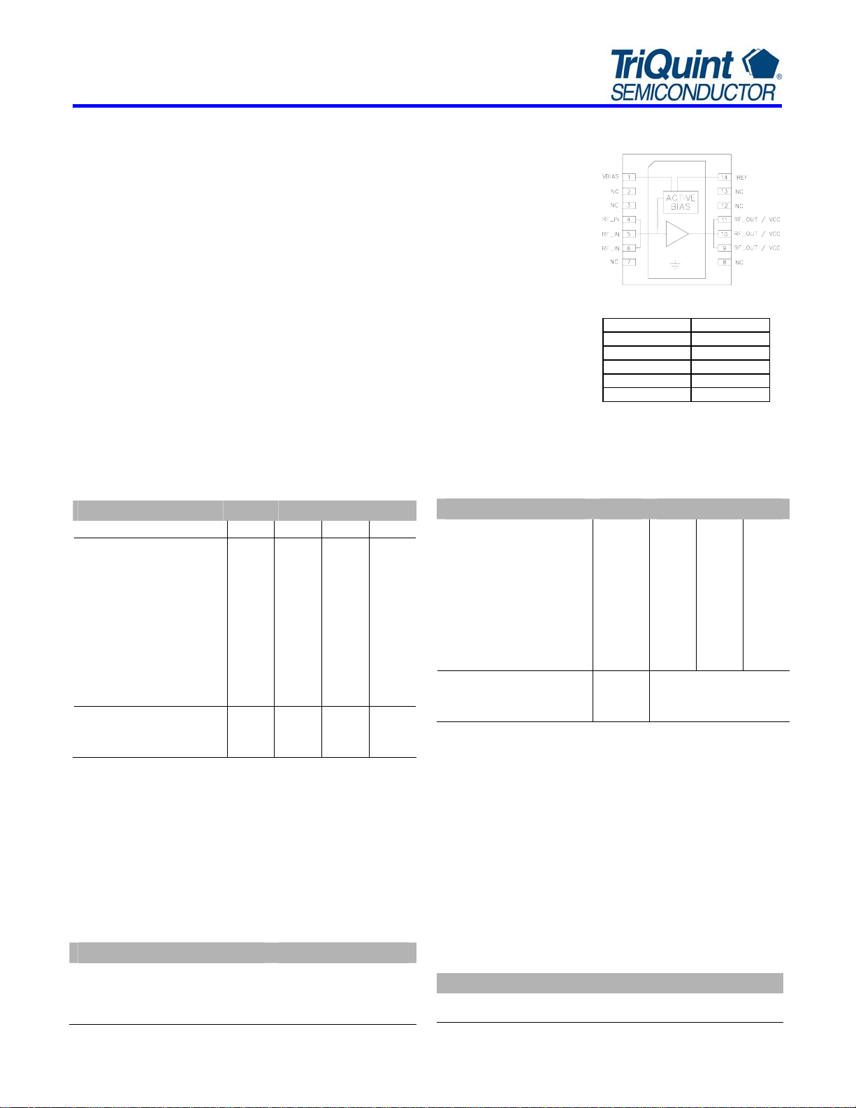
Functional Diagram
Function Pin No.
RFIN 4,5,6
RF
9,10,11
OUT
I
14
REF
V
1
BIAS
NC 2,3,7,8,12,13
Specifications and information are subject to change without notice
Page 2
AP562
3.3-3.8 GHz WiMAX 8W Power Amplifier
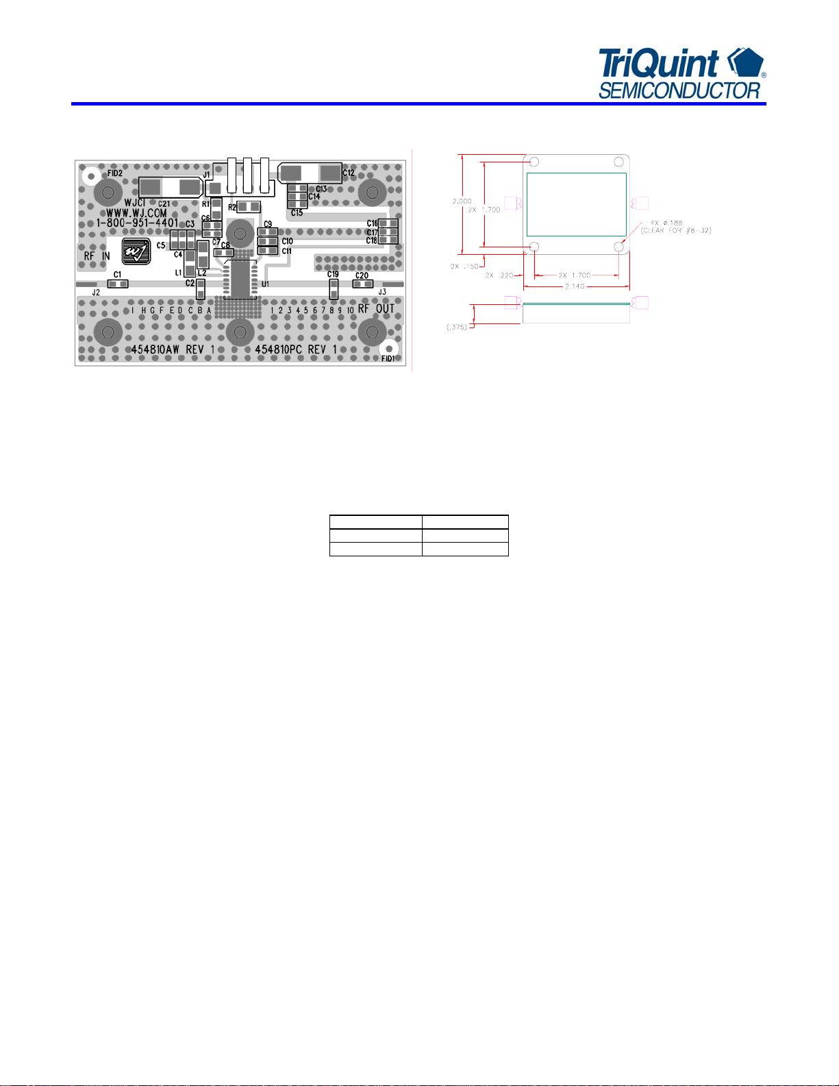
Application Circuit PC Board Layout
Vcc
Vpd
GND
Circuit Board Material: 0.0147” Rogers Ultralam 2000, single layer, 1 oz
copper, ε
= 2.45, Microstrip line details: width = .042”, spacing = .050”
r
Notes:
1. Please note that for reliable operation, the evaluation board will have to be mounted to a much
2. The area around the module underneath the PCB should not contain any soldermask in order to
3. For proper and safe operation in the laboratory, the power-on sequencing is recommended.
Baseplate Configuration
larger heat sink during operation and in laboratory environments to dissipate the power
consumed by the device. The use of a convection fan is also recommended in laboratory
environments.
maintain good RF grounding.
Evaluation Board Bias Procedure
Following bias procedure is recommended to ensure proper functionality of AP562 in a laboratory environment. The sequencing is not
required in the final system application.
Turn-on Sequence:
1. Attach input and output loads onto the evaluation board.
2. Turn on power supply Vcc = +12V.
3. Turn on power supply Vpd = +5V.
4. Turn on RF power.
Turn-off Sequence:
1. Turn off RF power.
2. Turn off power supply Vpd = +5V.
3. Turn off power supply Vcc = +12V.
Bias. Voltage (V)
Vcc +12
Vpd +5
TriQuint Semiconductor, Inc • Phone 1-800-9 51- 44 01 • FAX: 408-577-6633 • e-mail: info-sales@tqs.com • Web site: www.TriQuint.com Page 2 of 8 May 2009
Specifications and information are subject to change without notice
Page 3
AP562
3.3-3.8 GHz WiMAX 8W Power Amplifier
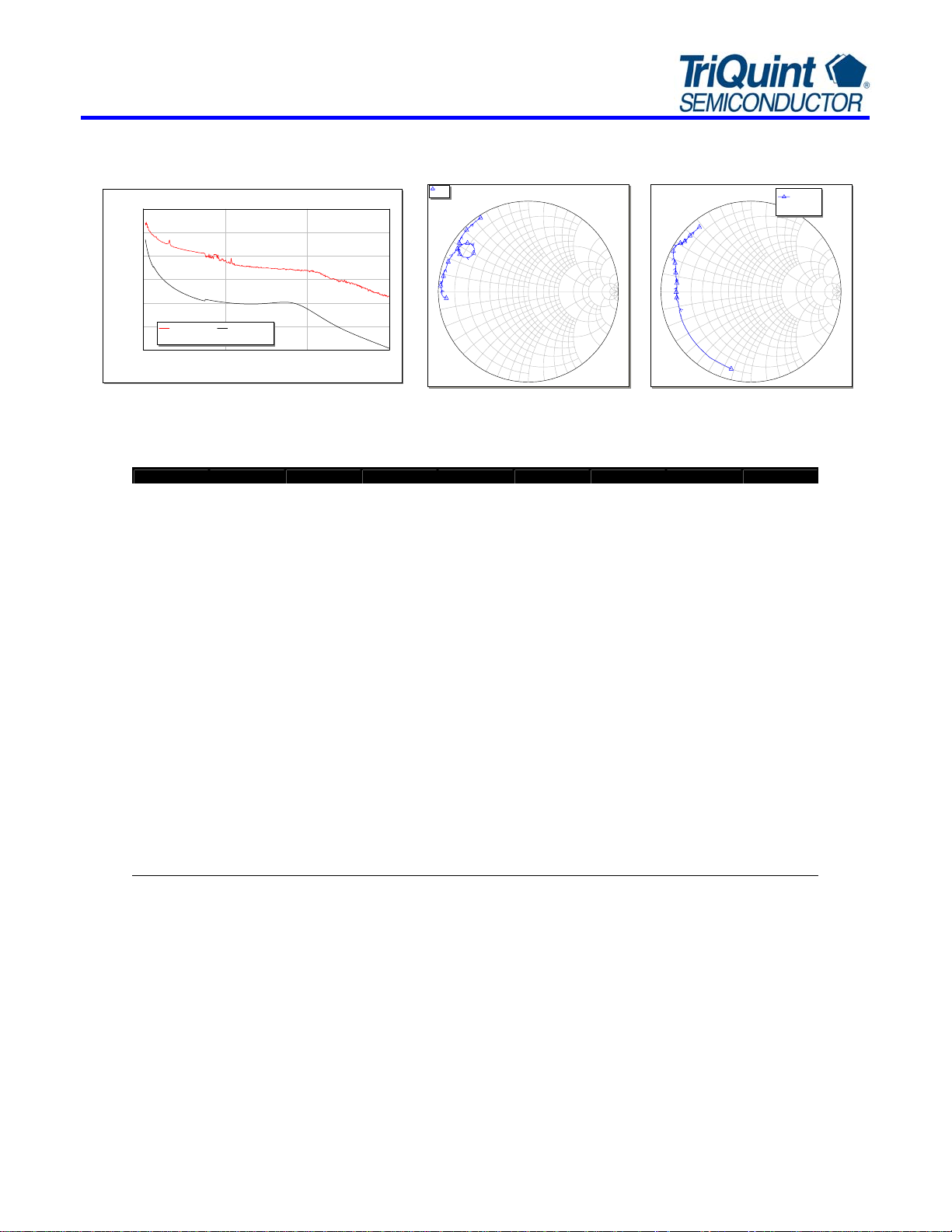
Typical Device Data
S-Parameters (VCC= +12 V, ICC = 400 mA, 25 °C, unmatched 50 ohm system)
S(1,1)
40
Gain / Maximum Stable Gain
30
20
10
Gain (dB)
0
-10
-20
DB(GMax())
AP562
0246
DB(|S(2,1)|)
AP562
Frequency (GHz)
AP562
4
.
0
2
.
0
0
0.2
2
.
0
-
4
.
0
-
Notes:
The gain for the unmatched device in 50 ohm system is shown as the trace in black color. For a tuned circuit for a particular frequency, it is expected that
actual gain will be higher, up to the maximum stable gain. The maximum stable gain is shown in the red line.
S-Parameters (VCC = +12 V, ICQ = 400 mA, 25 °C, unmatched 50 ohm system, calibrated to device leads)
Freq (MHz) S11 (dB) S11 (ang) S21 (dB) S21 (ang) S12 (dB) S12 (ang) S22 (dB) S22 (ang)
50 -0.79 -175.42 27.05 124.23 -41.01 40.51 -1.10 -104.38
100 -0.40 -177.67 22.28 107.37 -41.94 16.01 -1.53 -137.35
300 -0.31 179.53 14.07 90.92 -41.94 2.09 -1.68 -163.78
500 -0.29 177.89 9.72 82.63 -41.62 0.94 -1.77 -171.20
700 -0.29 175.84 6.87 75.39 -41.31 8.79 -1.81 -175.14
900 -0.34 173.80 4.76 69.22 -41.51 0.79 -1.71 -177.04
1100 -0.36 171.63 3.14 62.91 -41.31 -1.63 -1.63 -178.74
1300 -0.37 168.83 1.85 56.68 -41.31 -5.01 -1.60 179.84
1500 -0.35 165.93 0.86 50.02 -41.31 -8.04 -1.57 178.03
1700 -0.47 161.85 0.96 41.71 -40.35 -13.12 -1.66 174.97
1900 -0.50 158.09 0.45 34.33 -40.35 -18.22 -1.61 172.45
2100 -0.60 154.55 0.05 26.46 -40.18 -24.14 -1.51 170.10
2300 -0.69 150.84 -0.24 17.89 -40.09 -31.86 -1.38 167.43
2500 -0.82 147.61 -0.40 9.26 -39.83 -40.50 -1.28 164.93
2700 -0.94 144.72 -0.44 -0.25 -39.58 -51.10 -1.17 162.74
2900 -1.16 142.23 -0.27 -11.07 -39.33 -65.09 -1.02 160.45
3100 -1.51 140.70 -0.02 -23.54 -38.79 -81.01 -0.81 158.40
3300 -2.02 140.58 0.25 -38.88 -38.06 -102.23 -0.59 156.27
3500 -2.49 142.81 0.36 -58.18 -37.59 -129.91 -0.33 153.91
3700 -2.56 147.66 -0.16 -80.37 -37.20 -160.59 -0.23 150.78
3900 -2.06 151.40 -1.53 -102.11 -37.33 169.42 -0.28 148.13
4100 -1.43 151.78 -3.50 -120.64 -37.79 144.14 -0.40 146.26
4300 -1.01 150.24 -5.66 -135.37 -38.27 122.49 -0.53 145.38
4500 -0.76 148.06 -7.78 -147.04 -38.56 107.83 -0.64 144.44
Device S-parameters are available for download off of the website at: http://www.tqs.com
S11
8
1.0-1.0
.
0
6
.
0
1.0
0.4
0.6
0.8
6
.
0
-
8
.
0
-
Swp Max
6GHz
0
.
2
0
.
3
0
.
4
0
.
5
0
.
0
1
10.0
5.0
2.0
3.0
4.0
0
.
0
1
-
0
.
5
-
0
.
4
-
0
.
3
-
0
.
2
-
Swp Min
0.05GHz
4
.
0
2
.
0
0
0.2
2
.
0
-
4
.
0
-
S22
8
.
0
6
.
0
0.4
0.6
0.8
6
.
0
-
8
.
0
-
S(2,2)
1.0-1.0
AP562
0
.
2
1.0
5.0
2.0
3.0
4.0
0
.
2
-
Swp Max
0
.
3
4
0
0
.
3
-
Swp Min
0.05GHz
6GHz
0
.
0
.
5
0
.
0
1
10.0
0
.
0
1
-
0
.
5
-
.
4
-
TriQuint Semiconductor, Inc • Phone 1-800-9 51- 44 01 • FAX: 408-577-6633 • e-mail: info-sales@tqs.com • Web site: www.TriQuint.com Page 3 of 8 May 2009
Specifications and information are subject to change without notice
Page 4

AP562
3.3-3.8 GHz WiMAX 8W Power Amplifier
3.4-3.6 GHz Application Circuit (AP562-PCB3500)
Typical O-FDMA Performance at 25°C
Frequency (GHz) 3.4 3.5 3.6 Units
Channel Power +30 +30 +30 dBm
Power Gain 11.5 11.5 11.3 dB
Input Return Loss 11 15 15 dB
Output Return Loss 5.6 6.7 5.9 dB
EVM 2.2 1.9 1.7 %
Operating Current, Icc 720 685 670 mA
Collector Efficiency 11.1 11.7 12.2 %
Output P1dB 39.5 39.4 38.7 dBm
Quiescent Current, Icq 400
Vpd +5
Vcc +12
C21
C1
L3
R3
R1
D1
C6
C7
C8
C22
L3
C12
C13
D2
C14
C15
R2
C10
C11
C24
C23
3.4-3.6 GHz Application Circuit Performance Plots
802.16-2004 O-FDMA, 64QAM-1/2, 1024-FFT, 20 symbols and 30 subchannels. 9.5 dB PA R @ 0.01% , 5 MHz Carrier BW
Gain vs. Frequency
12
11
10
9
Gain (dB)
8
7
3 3.2 3.4 3.6 3.8 4
Efficiency vs Output Average Power vs. Frequency
20
15
10
5
Collector Efficiency (%)
0
20 22 24 26 28 30 32
T=25°C
Frequency (GHz)
T=25°C
3.4 GHz 3.5 GHz 3.6 GHz
Output Power (dBm)
mA
V
V
C16
C17
C18
C25
C20
Notes:
The primary RF microstrip line is 50 Ω.
Components shown on the silkscreen but not on the schematic are not used.
1. The edge of C23 is placed at 43mil from AP562 RFout pin.
2. The edge of C24 is placed right next to C23.
3. The edge of C22 is placed at 95mil from AP562 RFin pin.
4. The edge of L3 is placed right next to C22.
Return Loss
0
-5
-10
-15
S11, S22 (dB)
-20
-25
3 3.2 3.4 3.6 3.8 4
EVM vs. Output Average Power vs. Frequency
5
4
3
2
EVM (%)
1
0
20 22 24 26 28 30 32
T=25°C
S11 S22
Frequency (GHz)
T=25°C
3.4 GHz 3.5 GHz 3.6 GHz
Output Power (dBm)
Current vs Output Average Power vs. Frequency
800
750
700
650
600
550
500
Collector Current (mA)
450
400
20 22 24 26 28 30 32
13
12
Gain (dB)
11
10
-50-30-101030507090
T=25°C
3.4 GHz 3.5 GHz 3.6 GHz
Output Power (dBm)
Powe r Gain vs T e mperatu re
Pout = 30 dBm
3.4 GHz 3.5 GHz 3.6 GHz
Temperature (°C )
TriQuint Semiconductor, Inc • Phone 1-800-9 51- 44 01 • FAX: 408-577-6633 • e-mail: info-sales@tqs.com • Web site: www.TriQuint.com Page 4 of 8 May 2009
Specifications and information are subject to change without notice
Page 5

AP562
3.3-3.8 GHz WiMAX 8W Power Amplifier
Current vs Output Average Power vs Temperature
800
750
700
650
600
Icc (mA)
550
500
450
400
20 22 24 26 28 30 32
f=3.5 GHz
+25ºC -40ºC +85ºC
Output Power (dBm)
Efficiency vs Output Average Power vs Temperature
25
20
15
10
Efficiency (%)
5
0
20 22 24 26 28 30 32
f=3.5 GHz
+25ºC -40ºC +85ºC
Output Power (dBm)
EVM vs. Ou tput A verag e P ow e r vs Te m p erature
5
4
3
2
EVM (%)
1
0
20 22 24 26 28 30 32
f=3.5 GHz
+25ºC -40ºC +85ºC
Output Power (dBm)
TriQuint Semiconductor, Inc • Phone 1-800-9 51- 44 01 • FAX: 408-577-6633 • e-mail: info-sales@tqs.com • Web site: www.TriQuint.com Page 5 of 8 May 2009
Specifications and information are subject to change without notice
Page 6

AP562
3.3-3.8 GHz WiMAX 8W Power Amplifier
3.4 – 3.6 GHz Application Note: Changing Icq Biasing Configurations
The AP562 can be configured to operate with lower bias current by varying the bias-adjust resistor R2. (Table 1) The
recommended circuit configurations shown previously in this datasheet have the device operating with a 400 mA as the
quiescent current (I
upon the efficiency of the device, but degrade the EVM performance. Measured data shown in the plots below represents the
AP562 measured and configured for 3.5 GHz applications. It is expected that variation of the bias current for other frequency
applications will produce similar performance results.
Table 1 : Reduced Current Operation
Icq
(mA)
400
350
300
250
200
150
100
R2
(Ω)
270
275
320
380
473
616
857
). This biasing level represents a tradeoff in terms of EVM and efficiency. Lowering ICQ will improve
CQ
VPD
(V)
5
5
5
5
5
5
5
I
REF
(V)
2.92
2.88
2.83
2.8
2.73
2.66
2.6
EVM vs. Output Average Power vs. Icq
4
3
2
EVM (%)
1
100mA 150mA 200mA 250mA
300mA 350mA 400mA
0
28 29 30 31 32
f=3.5 GHz
Pout (dBm)
Efficiency vs. Output Average Power vs Icq
24
100mA 150mA 200mA 250mA
300mA 350mA 400mA
20
16
Efficiency (%)
12
8
28 29 30 31 32
f=3.5 GHz
Pout (dBm)
TriQuint Semiconductor, Inc • Phone 1-800-9 51- 44 01 • FAX: 408-577-6633 • e-mail: info-sales@tqs.com • Web site: www.TriQuint.com Page 6 of 8 May 2009
Specifications and information are subject to change without notice
Page 7

AP562
3.3-3.8 GHz WiMAX 8W Power Amplifier
Parameter Measurement Information
Switching Speed Test
Test Conditions:
Vcc = +12V at 25oC
Output Power = +30dBm @ 2.5 GHz
Rep Rate = 1 KHz, 50% duty cycle
Vpd amplitude = +5V
R2=200 ohms, C9=12pF
(C10, C11 removed for best switching
performance)
Xtal Detector Voltage =15mV (square law)
Test Result Waveforms:
Vpd = +5V
CW Signal Source
Vpd = +0V
Pulse Generator Oscilloscope
+ve
Vpd
AP56x Evaluation Brd
RF On
Cable Leng th = Lx
Cable Length = Lx
-ve
Cable Lengt h = Lx
Diode Detector
Attenuator
Vpd = +5V
RF Off
TriQuint Semiconductor, Inc • Phone 1-800-9 51- 44 01 • FAX: 408-577-6633 • e-mail: info-sales@tqs.com • Web site: www.TriQuint.com Page 7 of 8 May 2009
Delay = 50nS
Vpd = +5V
Delay = 50nS
RF On
Specifications and information are subject to change without notice
Page 8

AP562
3.3-3.8 GHz WiMAX 8W Power Amplifier
Mechanical Information
This package is lead-free/Green/RoHS-compliant. The plating material on the pins is annealed matte tin over copper. It is compatible with
both lead-free (maximum 260 °C reflow temperature) and leaded (maximum 245 °C reflow temperature) soldering processes.
Drawing
Outline Drawing
Product Marking
The component will be laser marked with a
“AP562-F” product label with an alphanumeric
lot code on the top surface of the package.
Tape and reel specifications for this part will be
located on the website in the “Application
Notes” section.
Functional Pin Layout
Mounting Configuration / Land Pattern
Pin Function
1 VBIAS
2, 3, 7, 8, 12, 13 N/C
4, 5, 6 RF IN
9, 10, 11 RF Output / Vcc
14 IREF
Backside paddle GND
MSL / ESD Rating
ESD Rating: Class 1A
Value: Passes 250V to <500V
Test: Human Body Model (HBM)
Standard: JEDEC Standard JESD22-A114
ESD Rating: Class IV
Value: Passes 1000V to <2000V
Test: Charged Device Model (CDM)
Standard: JEDEC Standard JESD22-C101
MSL Rating: Le vel 3 at +260 °C convection reflow
Standard: JEDEC Standard J-STD-020
TriQuint Semiconductor, Inc • Phone 1-800-9 51- 44 01 • FAX: 408-577-6633 • e-mail: info-sales@tqs.com • Web site: www.TriQuint.com Page 8 of 8 May 2009
Specifications and information are subject to change without notice
Page 9

 Loading...