

Page 1
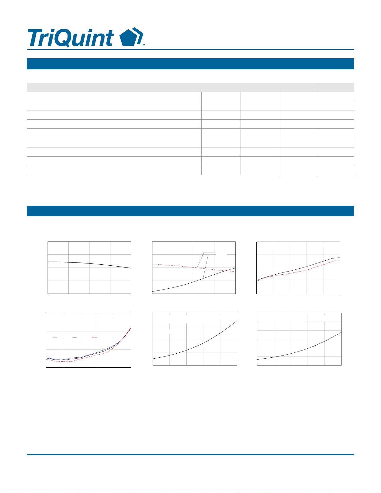
c
r
r
Applications
Small Cells / Repeaters / DAS
3G / 4G Wireless Infrastructure
Wireless Backhaul
Portable Radios
LTE / WCDMA / CDMA
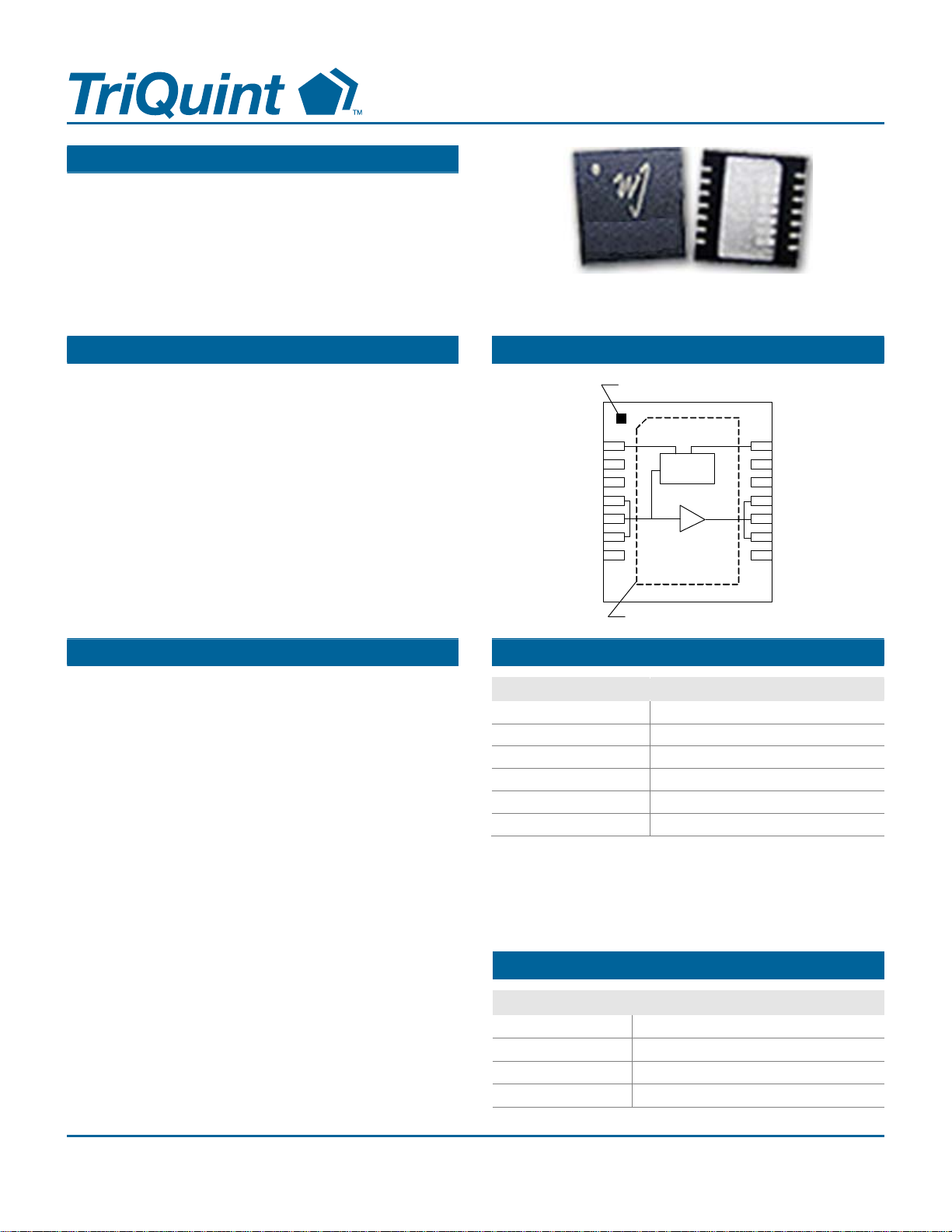
AP561-F
0.7-2.9 GHz 8W HBT Power Amplifier
14 Pin 5x6 mm DFN Package
Product Features
700-2900 MHz
+39 dBm P1dB
+12 V Supply Voltage
-50 dBc ACLR @ 28dBm Pout
1.5% EVM @ 30 dBm Pout
13 dB Gain @ 2.6GHz
Fast Shut-Down Capability
Internal Active Bias and Temp Compensation
Lead-free / RoHS-compliant
General Description
The AP561 is a high dynamic range broadband powe
amplifier in a surface mount package. The single-stage
amplifier has 13 dB Gain, while being able to achieve
high performance for 0.7–2.9 GHz applications with up
to +39 dBm of compressed 1dB power.
The AP561 uses a high reliability +12V InGaP/GaAs
HBT process technology. The device incorporates
proprietary bias circuitry to compensate for variations in
linearity and current draw over temperature. The device
does not require any negative bias voltage; an internal
active bias allows the AP561 to operate directly off a
commonly used +12V supply and has the added feature
of a +5V power down control pin. RoHS-compliant
5x6mm DFN package is surface mountable to allow fo
low manufacturing costs to the end user.
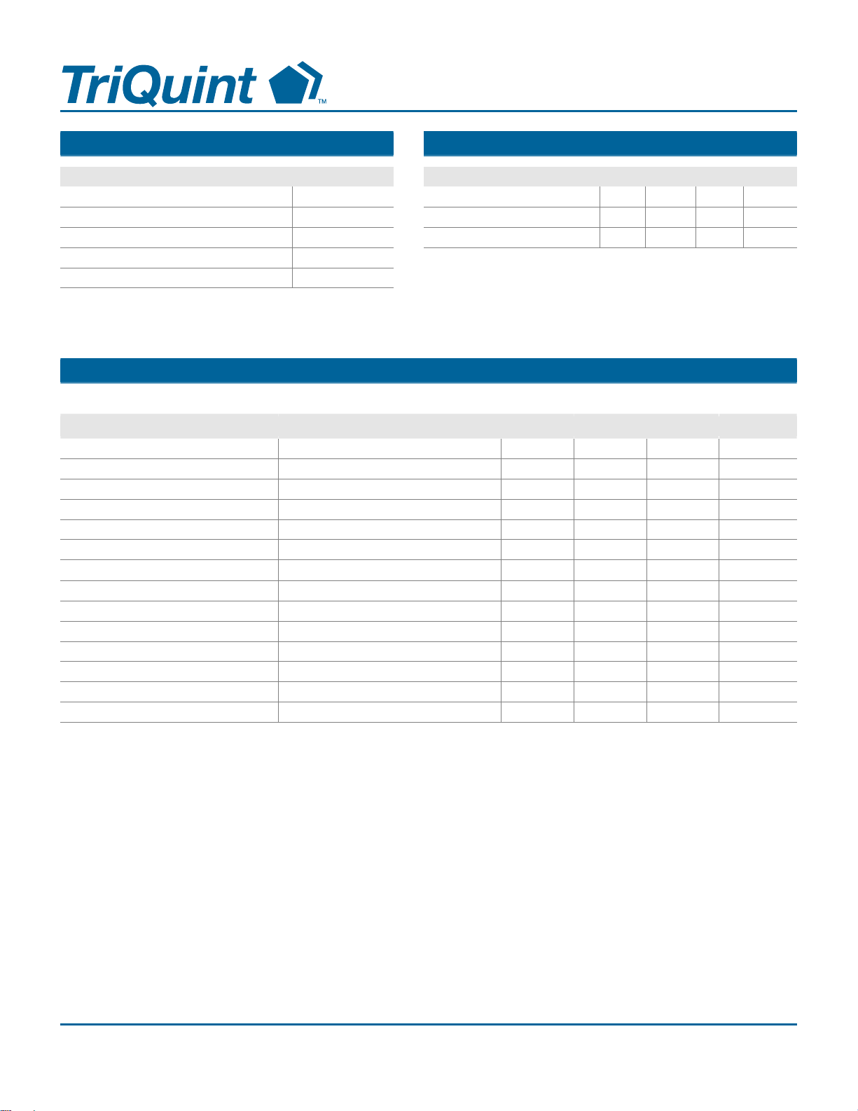
Functional Block Diagram
Pin 1 Reference Mark
1
PIN_Vbias
ACTIVE
BIAS
Backside Paddle - RF/DC GND
RFi n
RFi n
RFi n
2
NC
NC
3
4
5
6
NC
7
Pin Configuration
Pin No. Label
1 PIN_V
2, 3, 7, 8, 12, 13 N/C
4, 5, 6 RF IN
9, 10, 11 RF Output / VCC
14 PIN_VPD
Backside paddle RF / DC GND
BIAS
Ordering Information
14
13
12
11
10
9
8
PI N _ Vpd
NC
NC
RFout/ Vc
Rfout/ Vcc
Rfout/ Vcc
NC
Datasheet: Rev B 09-17-13
© 2013 TriQuint
Part No. Description
AP561-F 0.7-2.9 GHz 12V 8W Power Amplifier
AP561-PCB900 869-894 MHz Evaluation Board
AP561-PCB2140 2110-2170 MHz Evaluation Board
AP561-PCB2500 2.5-2.7 GHz Evaluation Board
Standard T/R size = 1000 pieces on a 7” reel
- 1 of 17 -
Disclaimer: Subject to change without notice
www.triquint.com
Page 2
Absolute Maximum Ratings
AP561-F
0.7-2.9 GHz 8W HBT Power Amplifier
Recommended Operating Conditions
Parameter Rating
Storage Temperature −55 to 150°C
RF Input Power, CW, 50Ω, T=25°C +33 dBm
Supply Voltage (VCC) +15 V
BV
cbo
Power Dissipation 14 W
Operation of this device outside the parameter ranges
given above may cause permanent damage.
+35 V
Parameter Min Typ Max Units
Supply Voltage (VCC) 12.0 V
T
−40 +85 °C
CASE
Tj for >106 hours MTTF 158 °C
Electrical specifications are measured at specified test conditions.
Specifications are not guaranteed over all recommended
operating conditions.
Electrical Specifications
Test conditions unless otherwise noted: VCC =+12V, VPD =+5V, Temp= +25°C, using AP561-PCB2600 application circuit
Parameter Conditions Min Typ Max Units
Operational Frequency Range
Test Frequency
Output Channel Power
Gain
Input Return Loss
Output Return Loss
Error Vector Magnitude
Collector Efficiency
RF Switching Speed
Output P1dB
Operating Current, ICC
Quiescent Current, ICQ
Reference Current, I
REF
Thermal Resistance, θjc
Notes:
1. Using an 802.16-2004 OFDMA, 64QAM-1/2, 1024-FFT, 20 symbols, 30 subchannels signal, 9.5 dB PAR @ 0.01%.
2. Switching speed: 50% TTL to 100/0% RF. Vpd used for device power down (low=RF off).
See note 1.
See note 2.
700 2900 MHz
2600
+30
13.0
14.5
6.5
1.7
16.2
50
+39
510
300
10
MHz
dBm
dB
dB
dB
%
%
ns
dBm
mA
mA
mA
Module (junction to case) 6.0 °C/W
Datasheet: Rev B 09-17-13
© 2013 TriQuint
- 2 of 17 -
Disclaimer: Subject to change without notice
www.triquint.com
Page 3
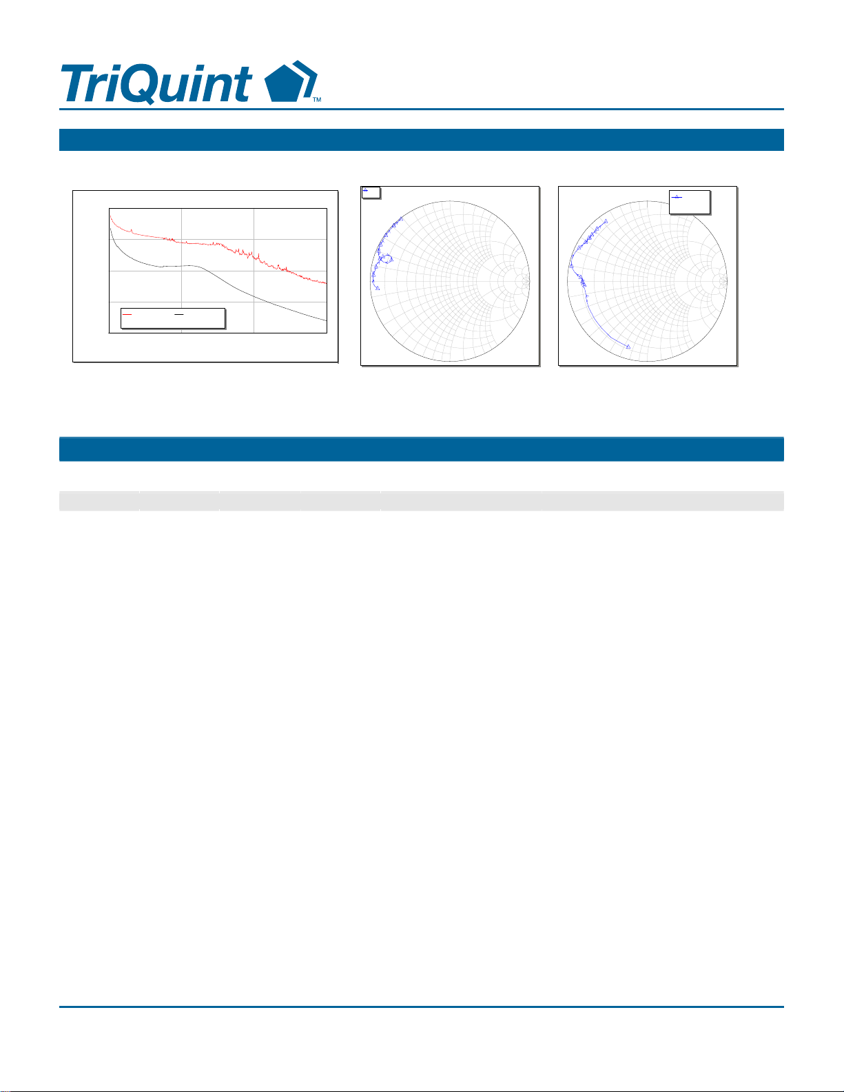
Device Characterization
AP561-F
0.7-2.9 GHz 8W HBT Power Amplifier
Test conditions unless otherwise noted: VCC =+12V, VPD =+5V, I
S(1,1)
40
Gain / Maximum Stable Gain
20
0
Gain (dB)
-20
DB(GMax())
AP561
-40
0246
DB(|S(2,1)|)
AP561
Frequency (GHz)
AP561
4
.
0
2
.
0
0
0.2
2
.
0
-
4
.
0
-
Notes:
= 300 mA (typ.), Temp= +25°C, calibrated to device pins
CQ
S11
8
1.0-1.0
.
0
6
.
0
1.0
0.4
0.6
0.8
6
.
0
-
8
.
0
-
Swp Max
6GHz
0
.
2
0
.
3
0
.
4
0
.
5
0
.
0
1
10.0
5.0
2.0
3.0
4.0
0
.
0
1
-
0
.
5
-
0
.
4
-
0
.
3
-
0
.
2
-
Swp Min
0.05GHz
4
.
0
2
.
0
0
0.2
2
.
0
-
4
.
0
-
S22
8
.
0
6
.
0
0.4
0.6
0.8
6
.
0
-
8
.
0
-
S(2,2)
1.0-1.0
AP561
1.0
2.0
Swp Max
6GHz
0
.
2
0
.
3
0
.
4
0
.
5
0
.
0
1
10.0
5.0
3.0
4.0
0
.
0
1
-
0
.
5
-
0
.
4
-
0
.
3
-
0
.
2
-
Swp Min
0.05GHz
The gain for the unmatched device in 50 ohm system is shown as the trace in black color. For a tuned circuit for a particular frequency,
it is expected that actual gain will be higher, up to the maximum stable gain. The maximum stable gain is shown in red.
S-Parameters
Test conditions unless otherwise noted: VCC =+12V, VPD =+5V, Temp= +25°C, 50 Ohm system
Freq (GHz) S11 (dB) S11 (ang) S21 (dB) S21 (ang) S12 (dB) S12 (ang) S22 (dB) S22 (ang)
50 -0.83 -174.19 27.09 122.75 -43.35 29.12 -1.38 -106.01
100 -0.43 -177.42 22.26 106.35 -43.10 8.71 -1.82 -138.64
300 -0.35 179.26 14.06 89.18 -41.21 1.08 -2.02 -164.78
500 -0.32 177.35 9.81 79.93 -40.63 0.69 -2.10 -172.01
700 -0.34 175.28 7.08 71.64 -40.35 3.54 -2.09 -176.13
900 -0.40 173.11 5.19 63.88 -40.26 -3.79 -1.99 -177.89
1100 -0.47 170.97 3.82 55.72 -40.09 -9.55 -1.86 -178.93
1300 -0.53 168.26 2.80 47.12 -39.83 -16.44 -1.78 -179.77
1500 -0.59 165.56 2.18 37.92 -39.58 -23.59 -1.68 179.34
1700 -0.87 161.87 2.75 25.71 -38.56 -35.47 -1.67 177.40
1900 -1.14 158.99 2.84 12.58 -37.79 -49.59 -1.45 176.17
2100 -1.58 157.33 3.04 -4.10 -37.20 -69.96 -1.07 174.50
2300 -2.07 158.08 3.08 -26.45 -36.71 -98.60 -0.57 171.36
2500 -2.11 161.67 2.27 -53.16 -36.83 -134.34 -0.20 166.20
2700 -1.52 163.86 0.21 -79.14 -37.65 -170.26 -0.18 160.52
2900 -0.93 162.94 -2.57 -100.12 -38.71 157.51 -0.38 155.92
3100 -0.60 161.26 -5.57 -115.90 -39.66 133.27 -0.55 152.79
3300 -0.44 159.75 -8.55 -127.57 -40.18 115.97 -0.68 150.56
3500 -0.30 157.96 -11.15 -136.15 -40.26 102.36 -0.77 148.63
3700 -0.20 156.27 -13.44 -143.55 -40.26 94.11 -0.84 147.06
3900 -0.16 154.67 -15.57 -150.57 -39.83 85.11 -0.87 145.70
4100 -0.14 152.82 -17.53 -157.27 -39.91 78.44 -0.87 144.40
4300 -0.15 150.80 -19.35 -163.61 -39.49 72.37 -0.86 143.38
4500 -0.13 148.32 -21.11 -170.25 -39.09 66.71 -0.89 142.13
Datasheet: Rev B 09-17-13
© 2013 TriQuint
- 3 of 17 -
Disclaimer: Subject to change without notice
www.triquint.com
Page 4
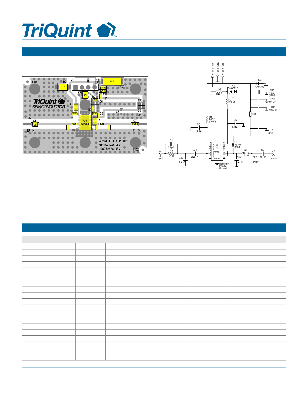
0.7-2.9 GHz 8W HBT Power Amplifier
AP561-PCB900 Evaluation Board (896−894 MHz)
Notes:
1. See Evaluation Board PCB Information section for material and stack-up.
2. All components are of 0603 size unless stated on the schematic.
3. The right edge of C20 is placed at 153 mil from the AP561 RFin pin.
4. The right edge of C21 is placed at 55 mil from the AP561 RFin pin.
5. The right edge of C24 is placed at 230 mil from the AP561 RFin pin.
6. The left edge of C22 is placed at 78 mil from the AP561 RFout pin.
7. The left edge of L2 is placed at 135 mil from the AP561 RFout pin.
8. The left edge of C23 is placed at 265 mil from the AP561 RFout pin.
9. Do not exceed 5.5V on Vpd or damage to D1 will occur. Do not exceed 13V on Vcc or damage to D2 will occur.
AP561-F
Bill of Material – AP561-PCB900
Reference Des. Value Description Manuf. Part Number
N/A N/A Printed Circuit Board – FR4
U1 N/A 0.7-2.9 GHz 8W Power Amplifier TriQuint AP561-F
C12 0.1 uF
C4, C11 1000 pF
C5, C18, C7 100 pF
C13 10 uF
R1 200 Ω
R7 330 Ω
R2 10 kΩ
R8 51 Ω
C1 22 pF
C20 10 pF
C21 1.5 Ω
C22 3.0 pF
C23, C24 6.8 pF
L2 1.5 nH
L1 18 nH
FB1 N/A
D1 N/A TVS Diode Array, 5V, SOT23, 2Ch
D2 N/A Diode TVS, 13V, 400W, 5% SMA On-Semiconductor
CAP, 0603,10%, 50V, X7R
CAP, 0603, 5%, 50V, NPO
CAP, 0603, 5%, 50V, NPO
CAP, 1206, 10%, 15V, Tantalum
RES, 0805, 5%, 1/10W. Chip.
RES, 0603,5%, 1/10W, Chip
RES, 0603, 5%,1/16W, Chip
RES, 0603, 5%, 1/16W, Chip
CAP, 0603, 5%, 50V, NPO/COG
CAP, 0603, 2%, ACCU-P, 50V
RES, 0603,5%, 1/10W, Chip
CAP, 0603, ± 0.05pF, ACCU-P, 50V
CAP, 0603, ± 0.05pF, ACCU-P, 50V
IND, 0603, ±0.3nH
IND, 0805, 5%, ceramic core
Filter EMI Ferrite Bead
various
various
various
various
various
various
various
various
various
AVX
various
AVX 06035J3R0ABSTR
AVX
Toko LL1608-FSL1N5S
Coilcraft
various
On-Semiconductor
06035J100GBSTR
0805HQ-18NXJC
SM05T1G
1SMA13AT3G
Datasheet: Rev B 09-17-13
© 2013 TriQuint
- 4 of 17 -
Disclaimer: Subject to change without notice
www.triquint.com
Page 5
Typical Performance – AP561-PCB900
AP561-F
0.7-2.9 GHz 8W HBT Power Amplifier
Test conditions unless otherwise noted: V
Parameter Typical Values
= +12 V, V
CC
= +5 V, I
PD
= 300 mA (typ.), Temp=+25°C
CQ
Units
Frequency 869 880 894 MHz
Gain 15.4 15.2 15.0 dB
Input Return Loss 18 15 13 dB
Output Return Loss 9 10 11 dB
ACLR @ 29dBm Output Power
IMD3 @ 29dBm Output Power
Operating Current, ICC @ 29dBm Output Power
Collector Efficiency @ 29dBm Output Power
[2]
-52 -52 -52 dBc
[1]
-46 -46.5 -47 dBc
[2]
470 465 460 mA
[2]
14 14.5 14.7 %
Output P1dB 39.2 39.1 38.9 dBm
Notes:
1. IMD3 is measured with 1 MHz tone spacing.
2. ACLR test set-up: 3GPP WCDMA, TM1+64DPCH, +5MHz Offset, PAR = 10.2 dB @ 0.01% Probability.
Performance Plots – AP561-PCB900
Test conditions unless otherwise noted: V
17
16
Gain vs. Frequency
Temp : +25 C
Vpd = 5V
= +12 V, V
CC
0
-5
= +5 V, I
PD
Return Loss vs. Frequency
Temp : +25 C
Vpd = 5V
= 300 mA (typ.), Temp=+25°C
CQ
-40
S22
S11
-45
IMD3 vs. Output Power
Frequency : 880 MHz
CW Signal
Temp.=+25oC
15
Gain (dB)
14
13
0.86 0.87 0.88 0.89 0.90
ACLR vs. Output Power vs. Frequency
-45
W-CDMA 3GPP Test Model 1+64 DPCH
PAR = 10.2dB @ 0.01% Probability
3.84 MHz BW
-50
869 MHz 880 MHz 894 MHz
ACLR (dBc)
-55
-60
20 22 24 26 28 30
Frequency (G Hz)
Temp.=+25oC
Output Power (dBm)
-10
Return Loss (dB)
-15
-20
0.86 0.87 0.88 0. 89 0.90
20
W-CDMA 3GPP Test Model 1+64 DPCH
PAR = 10.2dB @ 0.01% Probability
3.84 MHz BW
15
Temp.=+25oC
10
Efficiency (%)
5
0
20 22 24 26 28 30
Frequency ( GHz)
Efficiency vs. Output Power
Frequency : 880 MHz
Output Power (dBm)
-50
IMD3 (dBc)
-55
-60
20 22 24 26 28 30
600
W-CDMA 3GPP Test Model 1+64 DPCH
PAR = 10.2dB @ 0.01% Probability
3.84 MHz BW
550
500
450
Icc (mA)
400
350
300
20 22 24 26 28 30
Output Power/Tone (dBm)
Collector Current vs. Output Power
Frequency : 880 MHz
Output Power (dBm)
Datasheet: Rev B 09-17-13
© 2013 TriQuint
- 5 of 17 -
Disclaimer: Subject to change without notice
www.triquint.com
Page 6
0.7-2.9 GHz 8W HBT Power Amplifier
AP561-PCB2140 Evaluation Board (2110−2170 MHz)
FB1
AP561-F
R1
C20
Notes:
1. See Evaluation Board PCB Information section for material and stack-up.
2. All components are of 0603 size unless stated on the schematic.
3. The right edge of C20 is placed at 160 mil from the AP561 RFin pin.
4. The right edge of C21 is placed at 45 mil from the AP561 RFin pin.
5. The left edge of C22 is placed at 68 mil from the AP561 RFout pin.
6. The left edge of L2 is placed at 125 mil from the AP561 RFout pin.
7. The left edge of C23 is placed at 263 mil from the AP561 RFout pin.
8. Do not exceed 5.5V on Vpd or damage to D1 will occur. Do not exceed 13V on Vcc or damage to D2 will occur.
9. The primary RF microstrip line is 50. The RF trace is cut at component C21 and L2 for this particular reference design.
R7
C18
L1
C22
C23
Bill of Material – AP561-PCB2140
Reference Des. Value Description Manuf. Part Number
N/A N/A Printed Circuit Board – FR4
U1 N/A 0.7-2.9 GHz 8W Power Amplifier TriQuint AP561-F
C12 0.1 uF CAP, 0603,10%, 50V, X7R various
C4,C11 1000 pF CAP, 0603, 5%, 50V, NPO various
C5 100 pF CAP, 0603, 5%, 50V, NPO various
C13 10 uF CAP, 1206, 10%, 15V, Tantalum various
R1 200 Ω RES, 0805,5%,1/10W. CHIP. various
R7 280 Ω RES, 0603,5%, 1/10W, Chip various
R2 10 kΩ RES, 0603, 5%,1/16W, Chip various
C1, C7, C18 22 pF CAP, 0603, 5%, 50V, NPO/COG various
C20 2.4 pF CAP, 0603, ± 0.05 pF, ACCU-P, 50V AVX 06035J2R4ABSTR
C21 6.8 pF CAP, 0603, ± 0.1 pF, ACCU-P, 50V AVX 06035J6R8ABSTR
C22 3.9 pF CAP, 0603, ± 0.05pF, ACCU-P, 50V AVX 06035J3R9ABSTR
C23 2.0 pF CAP, 0603, ± 0.05pF, ACCU-P, 50V AVX 06035J2R0ABSTR
L2 1.2 nH IND, 0603, ±0.3nH Toko LL1608-FSL1N2S
L1 18 nH
IND, 0805, 5%, ceramic core
Coilcraft
FB1 N/A Filter EMI Ferrite Bead various
D1 N/A TVS Diode Array, 5V, SOT23, 2Ch
On-Semiconductor SM05T1G
D2 N/A Diode TVS, 13V, 400W, 5% SMA On-Semiconductor
0805HQ-18NXJC
1SMA13AT3G
Datasheet: Rev B 09-17-13
© 2013 TriQuint
- 6 of 17 -
Disclaimer: Subject to change without notice
www.triquint.com
Page 7

Typical Performance – AP561-PCB2140
AP561-F
0.7-2.9 GHz 8W HBT Power Amplifier
Test conditions unless otherwise noted: V
Parameter Typical Values
= +12 V, V
CC
= +5 V, I
PD
= 370 mA (typ.), Temp=+25°C
CQ
Units
Frequency 2110 2140 2170 MHz
Gain 12.4 12.4 12.3 dB
Input Return Loss 10 8 6.5 dB
Output Return Loss 6.3 8 11 dB
ACLR @ 28dBm Output Power
IMD3 @ 28dBm Output Power
Operating Current, ICC @ 28dBm Output Power
Collector Efficiency @ 28dBm Output Power
[2]
-48 -48 -48 dBc
[1]
-42.7 -42.3 -43.8 dBc
[2]
565 550 525 mA
[2]
9 9.5 10 %
Output P1dB 39.3 39.7 39.7 dBm
Notes:
1. IMD3 is measured with 1 MHz tone spacing.
2. ACLR test set-up: 3GPP WCDMA, TM1+64DPCH, +5MHz Offset, PAR = 10.2 dB @ 0.01% Probability.
Performance Plots – AP561-PCB2140
Test conditions unless otherwise noted: V
14
13
12
11
Gain (dB)
10
9
8
2.00 2.04 2.08 2.12 2.16 2. 20
-40
W-CDMA 3GPP Test Model 1+64 DPCH
PAR = 10.2dB @ 0.01% Probability
3.84 MHz BW
-45
-50
ACLR (dBc)
-55
-60
20 22 24 26 28 30 32
Gain vs. Frequency
Frequency ( GHz)
ACLR vs. Temperature
Frequency : 2.14 GHz
Output Power (dBm)
800
W-CDMA 3GPP Test Model 1+64 DPCH
PAR = 10.2dB @ 0.01% Probability
3.84 MHz BW
700
600
Icc(mA)
500
400
300
20 22 24 26 28 30
Temp : +25 C
Vpd = 5V
-40°C
+25
+85
Collector Current vs. Output Power
= +12 V, V
CC
Return Loss (dB)
°
C
°
C
ACLR (dBc)
Output Power (dBm)
= +5 V, I
PD
= 350 mA (typ.), Temp=+25°C
CQ
0
-3
-6
-9
-12
-15
2.00 2. 04 2.08 2.12 2.16 2. 20
-40
-45
-50
-55
-60
Return Loss vs. Frequency
Temp : +25 C
Vpd = 5V
Frequency ( GHz)
S22
S11
ACLR vs. Output Power vs. Frequency
W-CDMA 3GPP Test Model 1+64 DPCH
PAR = 10.2dB @ 0.01% Probability
3.84 MHz BW
2.11 GHz 2.14 GHz 2.17 GHz
20 22 24 26 28 30 32
Frequency : 2.14 GHz
Output Power (dBm)
Temp.=+25oC
-35
-40
-45
-50
IMD3 (dBc)
-55
-60
20 22 24 26 28 30
IMD3 vs. Output Power
Frequency : 2.14 GHz
CW Signal
41
40
39
38
37
P1dB (dBm)
36
35
2.11 2.12 2.13 2.14 2.15 2.16 2.17
20
W-CDMA 3GPP Test Model 1+64 DPCH
PAR = 10.2dB @ 0.01% Probability
3.84 MHz BW
15
Temp.=+25oC
10
Efficiency (%)
5
0
20 22 24 2 6 28 30 32
Output Power/Tone (dBm)
P1dB vs. Frequency
Temp.=+25oC
Frequency ( GHz)
Efficiency vs. Output Power
Frequency : 2.14 GHz
Output Power (dBm)
Temp.=+25oC
Datasheet: Rev B 09-17-13
© 2013 TriQuint
- 7 of 17 -
Disclaimer: Subject to change without notice
www.triquint.com
Page 8

0.7-2.9 GHz 8W HBT Power Amplifier
AP561-PCB2350 Evaluation Board (2300−2400 MHz)
R2
R1
200
10K
1
2
U
3
1
4
AP561
5
6
7
FB1
R1
C20
R7
C18
L1
C22
C23
C1
22 pF
R8
J2
RF
51
Input
2.0 pF
C20
C4
1000 pF
C21
5.6 pF
Notes:
1. See Evaluation Board PCB Information section for material and stack-up.
2. All components are of 0603 size unless stated on the schematic.
3. The right edge of C20 is placed at 123 mil from the AP561 RFin pin.
4. The right edge of C21 is placed at 45 mil from the AP561 RFin pin.
5. The left edge of C22 is placed at 30 mil from the AP561 RFout pin.
6. The left edge of C23 is placed at 280 mil from the AP561 RFout pin.
7. Do not exceed 5.5V on Vpd or damage to D1 will occur. Do not exceed 13V on Vcc or damage to D2 will occur.
8. The primary RF microstrip line is 50 . The RF trace is cut at component C21 for this particular reference design.
14
13
12
11
10
9
8
Backside
Paddle
Ground
AP561-F
D2
D1
SM05T1G
R7
280
C5
100 pF
L1
18 nH
(0805)
C22
3.0 pF
SMAJ33
FB1
C23
1.0 pF
C7
22 pF
C13
10 uF
6032
C12
0.1 uF
C11
1000 pF
C18
22 pF
Output
J3
RF
Bill of Material – AP561-PCB2350
Reference Des. Value Description Manuf. Part Number
N/A N/A Printed Circuit Board – FR4
U1 N/A 0.7-2.9 GHz 8W Power Amplifier TriQuint AP561-F
C1, C7, C18 22 pF Cap, Chip, 0603, 50V, 5%, NPO various
C5 100 pF Cap, Chip, 0603, 50V, 5%, NPO various
C4, C11 1000 pF Cap, Chip, 0603, 50V, 5%, NPO various
C12 0.1 uF Cap, Chip, 0603, 50V, 5%, NPO various
C13 10 uF Cap, Tantalum, 6032, 35V, 10% various
R2 10 KΩ Resistor, Chip, 0603, 5%, 1/16W various
R7 280 Ω Resistor, Chip, 0603, 1%, 1/16W various
R1 200 Ω Resistor, Chip, 0805, 1%, 1/16W various
FB1 N/A Ferrite Bead, 100 MHz various
C22 3.0 pF Cap, Chip, 0603, 50V, +/-0.05pF AVX 06035J3R0ABSTR
C21 5.6 pF Cap, Chip, 0603, 50V, +/-0.05pF AVX 06035J5R6ABSTR
C23 1.0 pF Cap, Chip, 0603, 50V, +/-0.05pF AVX 06035J1R0ABSTR
C20 2.0 pF Cap, Chip, 0603, 50V, +/-0.05pF AVX 06035J2R0ABSTR
L1 18 nH Ind, Chip, 0805, 5%, Ceramic Coilcraft
R8 51 Ω Resistor, Chip, 0603, 1%, 1/16W various
D1 N/A TVS Diode Array, 5V, SOT23, 2Ch On-Semiconductor SM05T1G
D2 N/A Diode TVS, 33V, 400W, 5% SMA On-Semiconductor 1SMA33AT3G
Datasheet: Rev B 09-17-13
© 2013 TriQuint
- 8 of 17 -
Disclaimer: Subject to change without notice
0805HQ-18NXJC
www.triquint.com
Page 9

Typical Performance – AP561-PCB2350
AP561-F
0.7-2.9 GHz 8W HBT Power Amplifier
Test conditions unless otherwise noted: V
Parameter Typical Values
= +12 V, V
CC
= +5 V, I
PD
= 340 mA (typ.), Temp=+25°C
CQ
Units
Frequency 2300 2350 2400 MHz
Gain 13.6 13.6 13.2 dB
Input Return Loss 21 23 14 dB
Output Return Loss 6.6 7 7 dB
EVM @ 28dBm Output Power
ACLR @ 28dBm Output Power
Operating Current, ICC @ 28dBm Output Power
Collector Efficiency @ 28dBm Output Power
[1]
1.6 1.4 1.1 %
[2]
-45.8 -47.0 -48.7 dBc
[2]
500 475 465 mA
[2]
10.7 11.1 11.5 %
Output P1dB 40.1 39.5 39.0 dBm
Notes:
1. 802.16-2004 O-FDMA, 64QAM-1/2, 1024-FFT, 20 symbols and 30 subchannels.10.2dB PAR @ 0.01%, 3.84 MHz Carrier BW
2. ACLR test set-up: 3GPP WCDMA, TM1+64DPCH, +5MHz Offset, PAR = 10.2 dB @ 0.01% Probability.
Performance Plots – AP561-PCB2350
Test conditions unless otherwise noted: V
16
14
12
Gain (dB)
10
8
2.30 2.32 2.34 2.36 2.3 8 2.40
-40
W-CDMA 3GPP Test Model 1+64 DPCH
PAR = 10.2dB @ 0.01% Probability
3.84 MHz BW
-45
-50
ACLR (dBc )
-55
-60
21 22 23 24 25 26 27 28 29 30
Gain vs. Frequency
Temp : +25 C
Vpd = 5V
Frequency (GHz)
ACLR vs. Frequency
Temp.=+25oC
2.3 GHz 2.35 GHz 2.4 GHz
Output Power (dBm)
= +12 V, V
CC
= +5 V, I
PD
= 340 mA (typ.), Temp=+25°C
CQ
0
-5
-10
-15
-20
Return Loss (dB)
-25
-30
2.30 2. 32 2.34 2.36 2.38 2.40
20
15
10
Efficiency (%)
5
0
20 22 24 26 28 30
2.5
2.0
Return Loss vs. Frequency
Temp : +25 C
Vpd = 5V
Frequency (GHz)
Efficiency vs. Output Power
W-CDMA 3GPP Test Model 1+64 DPCH
PAR = 10.2dB @ 0.01% Probability
3.84 MHz BW
Temp.=+25oC
Output Power (dBm)
EVM vs. Output Power
802.16-2004 O-FDMA, 64QAM-1/2, 1024FFT, 20 symbols and 30 subchannels.
10.2 dB PAR @ 0.01%, 3.84 MHz Carrier BW
S22
S11
Frequency : 2.35 GHz
41
40
39
38
37
P1dB (dBm)
36
35
2.30 2.32 2.34 2.36 2.3 8 2. 40
600
W-CDMA 3GPP Test Model 1+64 DPCH
PAR = 10.2dB @ 0.01% Probability
3.84 MHz BW
550
500
450
Icc (mA)
400
350
300
20 22 24 26 28 30
P1dB vs. Frequency
Temp.=+25oC
Frequency (GHz)
Collector Current vs. Output Power
Frequency : 2.35 GHz
Output Power (dBm)
Datasheet: Rev B 09-17-13
© 2013 TriQuint
1.5
1.0
EVM (%)
0.5
0.0
20 21 22 23 24 25 26 27 28 29 30
2.3GHz 2.35GHz 2.4GHz
Output Power (dBm)
- 9 of 17 -
Disclaimer: Subject to change without notice
www.triquint.com
Page 10

0.7-2.9 GHz 8W HBT Power Amplifier
AP561-PCB2500 Evaluation Board (2500−2700 MHz)
DNP
+ C12
D2
R4
C1
C2
R3
R2
R1
D1
C6
C7
C8
U1
AP561
C23
C24
C13
C14
C15
C16
C17
C10
C11
C25
C26
C27
C18
C28
C20
Notes:
1. See Evaluation Board PCB Information section for material and stack-up.
2. All components are of 0603 size unless stated on the schematic.
3. The right edge of C24 is placed at 85 mil from the AP561 RFin pin.
4. The left edge of C25 is placed at 55 mil from the AP561 RFout pin.
5. The left edge of C27 is placed at 175 mil from the AP561 RFout pin.
6. The DC bias feed is approximately a ¼ λ from output RF trace to C28.
7. Do not exceed 5.5V on Vpd or damage to D1 will occur. Do not exceed 13V on Vcc or damage to D2 will occur.
8. The primary RF microstrip line is 50. The RF trace is cut at component C21 for this particular reference design.
J1-2 Vpd
AP561-F
J1-3 GND
J1-4 Vcc
Bill of Material – AP561-PCB2500
Reference Des. Value Description Manuf. Part Number
N/A N/A Printed Circuit Board – Ultralam
U1 N/A 0.7-2.9 GHz 8W Power Amplifier TriQuint AP561-F
C6, C16 0.1 uF
C7, C10, C17 1000 pF
C8, C11, C18 100 pF
C12 10 uF
R1 200 Ω
R2 330 Ω
R3 10 kΩ
C1, C20, C28 22 pF
C23, C24, C25, C26 1.2 pF
C2 10 pF
C27 0.6 pF
R4 3.9 Ω
D1 N/A
D2 N/A
CAP, 0603,10%, 50V, X7R
CAP, 0603, 5%, 50V, NPO
CAP, 0603, 5%, 50V, NPO
CAP, 1206, 10%, 15V, Tantalum
RES, 0805, 5%, 1/10W. Chip
RES, 0603,5%, 1/10W, Chip
RES, 0603, 5%,1/16W, Chip
CAP, 0603, 5%, 50V, NPO/COG
CAP, 0603, ± 0.05 pF, ACCU-P, 50V
CAP, 0603, 5%, 50V, NPO
CAP, 0603, ± 0.05 pF, ACCU-P, 50V
RES, 0603, 5%, 1/16W, Chip
TVS Diode Array, 5V, SOT23, 2Ch
Diode TVS, 13V
various
various
various
various
various
various
various
various
AVX 06035J1R2ABSTR
various
AVX 06035J0R6ABSTR
various
On-Semiconductor SM05T1G
On-Semiconductor 1SMA33AT3G
Datasheet: Rev B 09-17-13
© 2013 TriQuint
- 10 of 17 -
Disclaimer: Subject to change without notice
www.triquint.com
Page 11

Typical Performance – AP561-PCB2500
AP561-F
0.7-2.9 GHz 8W HBT Power Amplifier
Test conditions unless otherwise noted: V
Parameter Typical Values
= +12 V, V
CC
= +5 V, I
PD
= 300 mA (typ.), Temp=+25°C
CQ
Units
Frequency 2500 2600 2700 MHz
Gain
Input Return Loss
Output Return Loss
EVM @ 30dBm Output Power
[1]
Operating Current, ICC @ 30dBm Output Power
Collector Efficiency @ 30dBm Output Power
[1]
Output P1dB
[1]
13.1 13.0 12.4
13 14.5 20
5.8 6.5 5
2.1 1.7 1.4
545 510 500
15.2 16.2 16.8
39.8 39.0 38.0
Notes:
1. 802.16-2004 O-FDMA, 64QAM-1/2, 1024-FFT, 20 symbols and 30 subchannels.PAR = 10.2dB@ 0.01%, 3.84 MHz Carrier BW
2. W-CDMA 3GPP, TM1+64DPCH, +5MHz Offset, PAR = 10.2 dB @ 0.01%, 3.84MHz BW
dB
dB
dB
%
mA
%
dBm
Performance Plots – AP561-PCB2500
Test conditions unless otherwise noted: V
15
14
13
12
Gain (dB)
11
10
9
2.50 2.55 2.60 2.65 2.70
-35
W-CDMA 3GPP Test Model 1+64 DPCH
PAR = 10.2dB @ 0.01% Probability
3.84 MHz BW
-40
-45
ACLR (dBc )
-50
-55
25 26 27 28 29 30 3 1
Gain vs. Frequency
Temp : +25 C
Frequency (GHz)
ACLR vs. Output Power vs. Frequency
Temp.=+25oC
2.5 GHz 2.6 GHz 2.7 GH z
Output Power (dBm)
= +12 V, V
CC
= +5 V, I
PD
= 300 mA (typ.), Temp=+25°C
CQ
0
-5
-10
-15
Return Loss (dB)
-20
-25
2.50 2.55 2.60 2.65 2.70
25
20
15
10
Efficiency (%)
5
0
25 26 27 28 29 30 3 1
3.0
2.5
2.0
1.5
EVM (%)
1.0
0.5
0.0
Return Loss vs. Frequency
Temp : +25 C
Frequency (GHz)
Efficiency vs. Output Power
W-CDMA 3GPP Test Model 1+64 DPCH
PAR = 10.2dB @ 0.01% Probability
3.84 MHz BW
Temp.=+25oC
Output Power (dBm)
EVM vs. Output Power
802.16-2004 O-FDMA, 64QAM-1/2, 10 24-FFT,
20 symbols and subchannels.
PAR = 10.2dB @ 0.01%, 3.84 MHz Carrier BW
2.5 GHz 2.6 GH z 2. 7 GHz
25 26 27 28 29 30 31
Output Power (dBm)
S22
S11
Frequency : 2.6 GHz
Temp.=+25oC
42
40
38
36
P1dB (dBm)
34
32
2.50 2.55 2.60 2.65 2.70
600
W-CDMA 3GPP Test Model 1+64 DPCH
PAR = 10.2dB @ 0.01% Probability
550
3.84 MHz BW
500
450
Icc (mA)
400
350
300
25 26 27 28 29 30 31
P1dB vs. Frequency
Temp.=+25oC
Frequency (GHz)
Collector Current vs. Output Power
Frequency : 2.6 GHz
Temp=+25 C
Output Power (dBm)
Datasheet: Rev B 09-17-13
© 2013 TriQuint
- 11 of 17 -
Disclaimer: Subject to change without notice
www.triquint.com
Page 12

AP561-F
0.7-2.9 GHz 8W HBT Power Amplifier
Reference Design 2500-2700 MHz: Changing Icq Biasing Configurations
The AP561 can be configured to operate with lower bias current by varying the bias-adjust resistor R2. (Error! Not a
valid bookmark self-reference.) The recommended circuit configuration has the device operating with a 300 mA as
the quiescent current (ICQ). This biasing level represents a tradeoff in terms of EVM and efficiency. Lowering ICQ will
improve upon the efficiency of the device, but degrade the EVM performance. Measured data shown in the plots
below represents the AP561-PCB2500 measured and configured for 2.6GHz applications. It is expected that variation
of the bias current for other frequency applications will produce similar performance results.
Table 1 : Reduced Current Operation
ICQ (mA) R2 (Ω) VPD (V) I
300 330 5 2.85
280 336 5 2.81
260 340 5 2.78
240 343 5 2.76
220 348 5 2.73
200 351 5 2.71
REF
(V)
EVM (%)
EVM vs. Output Average Power vs. Icq
5
200mA 220mA 240mA
4
260mA 280mA 300mA
3
2
1
0
20 22 24 26 28 30 32 34
Freq = 2.6 GHz, T= 25ºC
Output Power (dBm)
14
13
12
11
Gain (dB)
10
9
2.4 2.5 2.6 2.7 2.8
Datasheet: Rev B 09-17-13
© 2013 TriQuint
Power Gain vs.Frequency vs. Icq
Vcc = 12V, T= 25ºC
200mA 220mA 240mA
260mA 280mA 300mA
Frequency (GHz)
Efficiency vs. Output Average Power vs Icq
30
25
20
15
10
Efficiency (%)
5
0
20 22 24 26 28 30 32 34
Freq = 2.6 GHz, T= 25ºC
200mA 220mA 240mA
260mA 280mA 300mA
Output Power (dBm)
700
600
500
400
Icc (mA)
300
200
20 22 24 26 28 30 32 34
- 12 of 17 -
Power Gain vs. Output Average Power vs. Icq
14
13
12
11
Gain (dB)
10
9
20 22 24 26 28 30 32
Icc vs. Output Average Power vs. Icq
Freq = 2.6 GHz, T= 25ºC
200mA 220mA 240mA
260mA 280mA 300mA
Output Power (dBm)
Disclaimer: Subject to change without notice
Freq = 2.6GHz, T= 25ºC
200mA 220mA 240mA
260mA 280mA 300mA
Output Power (dBm)
www.triquint.com
Page 13

0.7-2.9 GHz 8W HBT Power Amplifier
e
-ve
d
Parameter Measurement Information: Switching Speed Test
AP561-F
Test Conditions:
Vcc = +12V at 25°C
Output Power = +30dBm at 2.5 GHz
Rep Rate = 1 KHz, 50% duty cycle
Vpd amplitude = +5V
R2 = 200Ω, C9 = 12pF
(C10, C11 removed for best switching
performance)
Xtal Detector Voltage =15mV (square law)
Test Result Waveforms:
Vpd = 5V
CW Signal Source
Vpd = 0V
Cable Length = Lx
Puls e Gene r ato r Oscillosco pe
+v
Cabl e L en gt h = Lx
Vp
AP56x Evaluation Brd
A ttenu ator
Cable Length = Lx
D io de Dete cto r
RF Off
Datasheet: Rev B 09-17-13
© 2013 TriQuint
Delay = 50nS
Vpd = 5V
RF On
- 13 of 17 -
Vpd = 5V
RF On
Delay = 50nS
Disclaimer: Subject to change without notice
www.triquint.com
Page 14

AP561-F
0.7-2.9 GHz 8W HBT Power Amplifier
Evaluation Board Bias Procedure
Following bias procedure is recommended to ensure proper functionality of AP561 in a laboratory environment. The
sequencing is not required in the final system application.
Bias. Voltage (V)
VCC +12
VPD +5
Turn-on Sequence:
1. Attach input and output loads onto the evaluation board.
2. Turn on power supply VCC = +12V.
3. Turn on power supply VPD = +5V.
4. Turn on RF power.
Turn-off Sequence:
1. Turn off RF power.
2. Turn off power supply VPD = +5V.
3. Turn off power supply VCC = +12V.
Datasheet: Rev B 09-17-13
© 2013 TriQuint
- 14 of 17 -
Disclaimer: Subject to change without notice
www.triquint.com
Page 15

Pin Configuration and Description
AP561-F
0.7-2.9 GHz 8W HBT Power Amplifier
Pin No. Label Description
1 PIN_V
2, 3, 7, 8, 12, 13 N/C
4, 5, 6 RF IN RF Input. DC Voltage present, blocking cap required. Requires matching for operation.
9, 10, 11 RF Output / VCC RF Output. DC Voltage present, blocking cap required
14 PIN_VPD
Backside Paddle RF/DC GND
Voltage supply for active bias for the amp. Connect to same supply voltage as Vcc.
BIAS
No internal connection. This pin can be grounded or N/C on PCB. Land pads should be provided for PCB
mounting integrity.
Reference current into internal active bias current mirror. Current into PIN_VPD sets device quiescent
current. Also, can be used as on/off control.
Multiple Vias should be employed to minimize inductance and thermal resistance. Use recommended via
pattern shown under mounting configuration and ensure good solder attach for optimum thermal and
electrical performance
Evaluation Board PCB Information
TriQuint PCB 1069110 Material and Stack-up
Ultralam
1 oz. Cu top layer
0.0147 ± 0.0015
Finished Board
Thickness
Ultralam 2000
=2.5 typ.
ε
r
TriQuint PCB 1080526 Material and Stack-up
0.021 ± 0.002
Finished Board
Thickness
Datasheet: Rev B 09-17-13
© 2013 TriQuint
FR4
Nelco N-4000-13
=3.7 typ.
ε
r
1 oz. Cu bottom layer
1 oz. Cu top layer
1 oz. Cu bottom layer
- 15 of 17 -
Disclaimer: Subject to change without notice
www.triquint.com
Page 16

Mechanical Information
Package Marking and Dimensions
Marking: Part number – AP561-F
Lot code – XXXX
AP561-F
0.7-2.9 GHz 8W HBT Power Amplifier
Notes:
1. All dimensions are in millimeters. Angles are in degrees.
2. Except where noted, this part outline conforms to JEDEC standard MO-220, Issue E (Variation VGGC) for thermally enhanced
plastic very thin fine pitch quad flat no lead package (QFN).
3. Dimension and tolerance formats conform to ASME Y14.4M-1994.
4. The terminal #1 identifier and terminal numbering conform to JESD 95-1 SPP-012.
PCB Mounting Pattern
Notes:
1. All dimensions are in millimeters. Angles are in degrees.
2. Use 1 oz. copper minimum for top and bottom layer metal.
3. Vias are required under the backside paddle of this device for proper RF/DC grounding and thermal dissipation. We
recommend a 0.35mm (#80/.0135") diameter bit for drilling via holes and a final plated thru diameter of 0.25 mm (0.10”).
4. Ensure good package backside paddle solder attach for reliable operation and best electrical performance.
Datasheet: Rev B 09-17-13
© 2013 TriQuint
- 16 of 17 -
Disclaimer: Subject to change without notice
www.triquint.com
Page 17

r
Product Compliance Information
AP561-F
0.7-2.9 GHz 8W HBT Power Amplifier
ESD Sensitivity Ratings
Caution! ESD-Sensitive Device
ESD Rating: Class 1A
Value: Passes ≥ 250 V to < 500 V
Test: Human Body Model (HBM)
Standard: JEDEC Standard JESD22-A114
ESD Rating: Class IV
Value: Passes 1000 V to <2000 V
Test: Charged Device Model (CDM)
Standard: JEDEC Standard JESD22-C101
MSL Rating
MSL Rating: Level 3
Test: 260°C convection reflow
Standard: JEDEC Standard IPC/JEDEC J-STD-020
Contact Information
Solderability
Compatible with both lead-free (260 °C max. reflow
temperature) and tin/lead (245 °C max. reflow
temperature) soldering processes.
Contact plating: Annealed Matte Tin over Cu
RoHs Compliance
This part is compliant with EU 2002/95/EC RoHS
directive (Restrictions on the Use of Certain Hazardous
Substances in Electrical and Electronic Equipment).
This product also has the following attributes:
Lead Free
Halogen Free (Chlorine, Bromine)
Antimony Free
TBBP-A (C15H12Br402) Free
PFOS Free
SVHC Free
For the latest specifications, additional product information, worldwide sales and distribution locations, and information
about TriQuint:
Web: www.triquint.com Tel: +1.503.615.9000
Email: info-sales@triquint.com Fax: +1.503.615.8902
For technical questions and application information: Email: sjcapplications.engineering@triquint.com
Important Notice
The information contained herein is believed to be reliable. TriQuint makes no warranties regarding the information
contained herein. TriQuint assumes no responsibility or liability whatsoever for any of the information contained
herein. TriQuint assumes no responsibility or liability whatsoever for the use of the information contained herein. The
information contained herein is provided "AS IS, WHERE IS" and with all faults, and the entire risk associated with
such information is entirely with the user. All information contained herein is subject to change without notice.
Customers should obtain and verify the latest relevant information before placing orders for TriQuint products. The
information contained herein or any use of such information does not grant, explicitly or implicitly, to any party any
patent rights, licenses, or any other intellectual property rights, whether with regard to such information itself o
anything described by such information.
TriQuint products are not warranted or authorized for use as critical components in medical, life-saving, or lifesustaining applications, or other applications where a failure would reasonably be expected to cause severe personal
injury or death.
Datasheet: Rev B 09-17-13
© 2013 TriQuint
- 17 of 17 -
Disclaimer: Subject to change without notice
www.triquint.com
Page 18

 Loading...