

Page 1

Low-Power Off-line Primary Side Regulation Controller AP3772
Advance Datasheet
General Description
The AP3772 is a high performance AC/DC power
supply controller for battery charger and adapter
applications. The device uses Pulse Frequency
Modulation (PFM) method to build discontinuous
conduction mode (DCM) flyback power supplies.
The AP3772 provides accurate constant voltage,
constant current (CV/CC) regulation without
requiring an opto-coupler and the secondary control
circuitry. It also eliminates the need of loop
compensation circuitry while maintaining good
stability. The AP3772 can achieve excellent
regulation and high average efficiency, yet meets
no-load consumption less than 30mW. It can also
achieve excellent dynamic performance while
maintaining 30mW standby power with AP4340.
The AP3772 has a built-in fixed cable voltage drop
compensation function. The magnitude of the cable
compensation voltage is set as 6%, 3% and 0 of the
rated output voltage respectively to meet various
cables with different length and gauge. It also has an
adjustable built-in line compensation function to
achieve tight CC.
The AP3772 is available in SOT-23-6 package.
Features
• Primary Side Control for Tight Constant Current
and Constant Voltage
• 30mW No-load Input Power
• Excellent Dynamic Performance with AP4340
• Bipolar Junction Transistor (BJT) Driving
• Proprietary Adjustable Line Compensation for
CC Variation
• Constant and Built-in 6%, 3% and No Cable
Voltage Drop Compensation
• Enhanced Audio Noise Suppression
• Open Circuit Protection
• Over Voltage Protection
• Short Circuit Protection
• SOT-23-6 package
Applications
• Adapters/Chargers for Cell/cordless Phones,
PDAs, MP3 and Other Portable Devices
• LED Driver
• Standby and Auxiliary Power Supplies
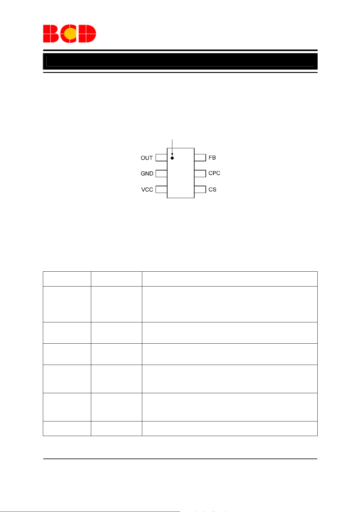
Figure 1. Package Type of AP3772
SOT-23-6
Dec. 2011 Rev. 1. 0 BCD Semiconductor Manufacturing Limited
1
Page 2
Advance Datasheet
Low-Power Off-line Primary Side Regulation Controller AP3772
Pin Configuration
K6 Package
(SOT-23-6)
Pin 1 Mark
1
2
34
Figure 2. Pin Configuration of AP3772 (Top View)
6
5
Pin Description
Pin Number Pin Name Function
The OUT pin is used to turn on and turn off the power switch. When
turning on the power switch, the OUT pin will output 30mA source
1 OUT
2 GND
3 VCC
4 CS
5 CPC
6 FB
current to support the base current of the power BJT. When turning
off the power switch, the resistance between the OUT and GND will
become to 5Ω
The GND pin is the ground of the IC. When the power BJT is turned
off, a fast reverse sinking current to the gate of BJT will flow out
from this pin. Attention should be paid to in the PCB layout
The VCC pin supplies the power for the IC. In order to get the
correct operation of the IC, a capacitor with low ESR should be
placed as close as possible to the VCC pin
The CS is the current sense pin of the IC. The IC will turn off the
power BJT according to the voltage on the CS pin. When the power
BJT is on, a current is output from the CS pin which is proportional
to the line voltage to realize the function of line compensation
A capacitor more than 10nF should be connected to this pin. The
voltage of CPC pin is linear to load of the system and it is used for
the functions of cable voltage drop compensation and audio noise
suppression
The CV and CC regulation are realized based on the voltage
sampling of this pin
Dec. 2011 Rev. 1. 0 BCD Semiconductor Manufacturing Limited
2
Page 3
Advance Datasheet
Low-Power Off-line Primary Side Regulation Controller AP3772
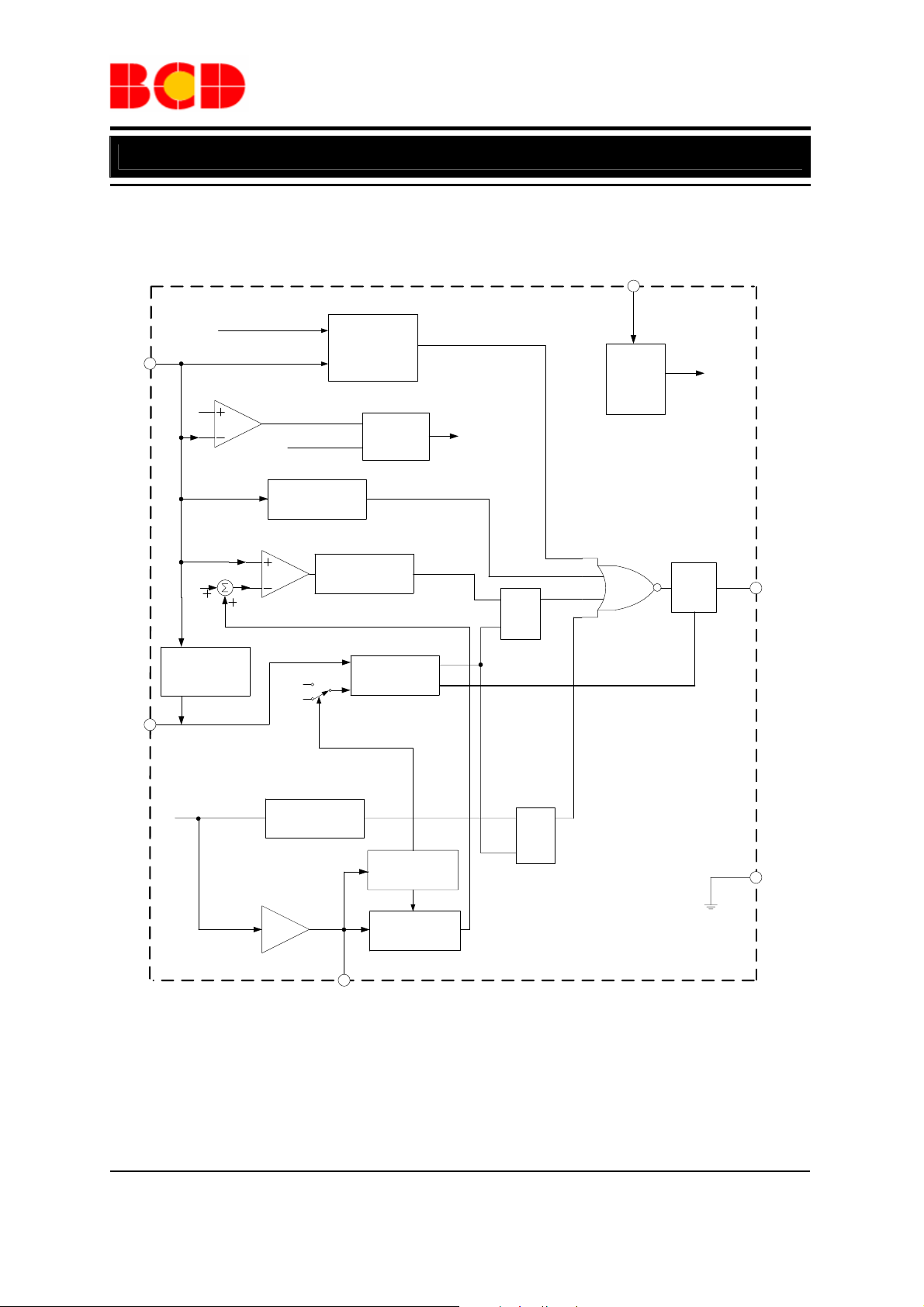
Functional Block Diagram
VCC
3
FB
UVLO
6
0.1V
COMP
PFM
OVP
&
OCKP
Tonsec
Detector
PRO
T
ONS
Regulator
&
Bias
UVLO
CS
V
FB
Line
Compensation
4
T
ONS
Dynamic
Response
Constant Voltage
EA
V
REF1
V
REF2
Constant Current
Control
Control
Peak Current
Control & LEB
Audio noise
Suppression
Cable
Compensation
Q
R
S
Shutdown
Pre_Shutdown
Q
R
S
CV_
CC_
CC
Pro
Dyn
ctrl
ctrl
_ctrl
PFM
Driver
1
OUT
2
GND
5
CPC
Figure 3. Functional Block Diagram of AP3772
Dec. 2011 Rev. 1. 0 BCD Semiconductor Manufacturing Limited
3
Page 4
Advance Datasheet
Low-Power Off-line Primary Side Regulation Controller AP3772
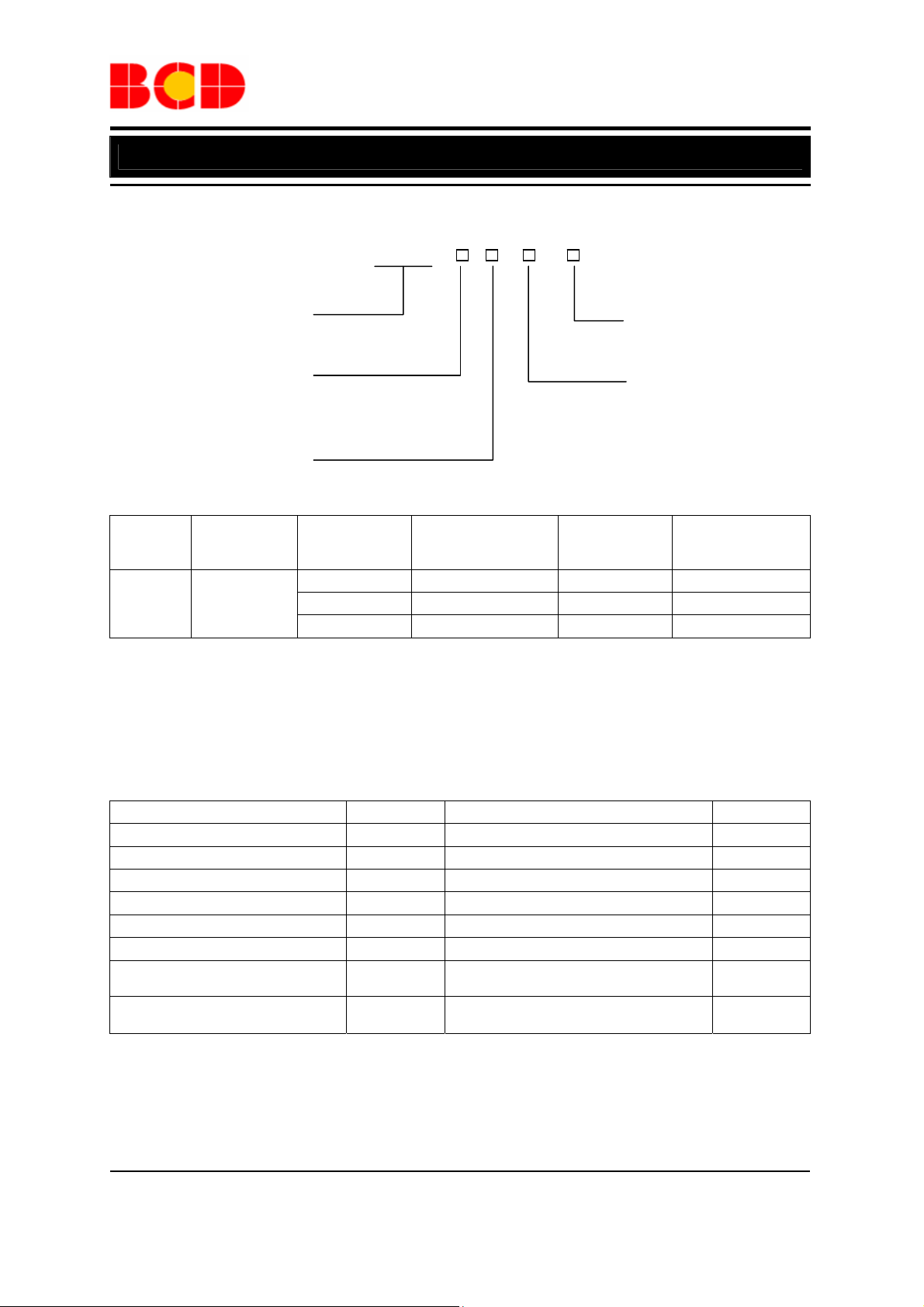
Ordering Information
AP3772 -
Circuit Type
G1: Green
Cable Compensation Voltage
A: 6%
B: 3%
C: 0
Package
K6: SOT-23-6
TR: Tape & Reel
Package
SOT-23-6
BCD Semiconductor's Pb-free products, as designated with "G1" suffix in the part number, are RoHS compliant
and green.
Temperature
Range
-40 to 85°C
Cable
Compensation
Voltage
6% AP3772AK6TR-G1 GKA Tape & Reel
3% AP3772BK6TR-G1 GKB Tape & Reel
0 AP3772CK6TR-G1 GKC Tape & Reel
Part Number Marking ID Packing Type
Absolute Maximum Ratings (Note 1)
Parameter Symbol Value Unit
Supply Voltage VCC -0.3 to 30 V
CS, CPC to GND -0.3 to 7 V
FB Input Voltage VFB -40 to 10 V
Source Current at OUT Pin I
Operating Junction Temperature TJ 150 ºC
Storage Temperature T
Lead Temperature (Soldering, 10
sec)
Thermal Resistance (Junction to
Ambient)
Internally Limited A
SOURCE
-65 to 150 ºC
STG
T
300 ºC
LEAD
θ
JA
200 ºC/W
Note 1: Stresses greater than those listed under “Absolute Maximum Ratings” may cause permanent damage to
the device. These are stress ratings only, and functional operation of the device at these or any other conditions
beyond those indicated under “Recommended Operating Conditions” is not implied. Exposure to “Absolute
Maximum Ratings” for extended periods may affect device reliability.
Dec. 2011 Rev. 1. 0 BCD Semiconductor Manufacturing Limited
4
Page 5

Advance Datasheet
Low-Power Off-line Primary Side Regulation Controller AP3772
Electrical Characteristics
V
=15V, TA=25°C, unless otherwise specified.
CC
Parameter Symbol Conditions Min Typ Max Unit
UVLO SECTION
Startup Threshold VTH (ST) 13 15.5 18
Minimal Operating Voltage V
(MIN) 3 3.5 6.5
OPR
STANDBY CURRENT SECTION
Startup Current IST
V
CC=VTH
Before startup
(ST)-1V,
0 0.2 0.6
Operating Current ICC(OPR) Static current 250 500 600
DRIVE OUTPUT SECTION
Output Current
Sink I
Source I
Maximum Off Time t
Apply 1V @OUT pin 150 330 500 mA
SINK
24 30 40 mA
SOURCE
(MAX) 18 ms
OFF
CURRENT SENSE SECTION
Current Sense Threshold
Voltage at Heavy Load
Leading Edge Blanking t
500 525 550 mV
V
CS1
The minimum power
LEB
switch turn on time
300 500 650 ns
FEEDBACK INPUT SECTION
Input Resistance of FB Pin RFB VFB=4V 1 1.6 2
Feedback Threshold VFB 3.98 4.04 4.1 V
LINE COMPENSATION SECTION
Line Compensation Current I
VFB=-5V 6
LINE
CABLE COMPENSA TION SECTION
Cable Compensation
Voltage
FB
_CABLE/VFB
%
AP3772B 2 3 4 %
AP3772C 0 %
AP3772A 5 6 7 %
∆V
DYNAMIC FUNCTION SECTION
Delay Time for Dynamic
Function
Trigger Voltage for
Dynamic Function
t
110 150 200 µs
D
V
120 150 180 mV
TRIGGER
PROTECTION SECTION
Over Voltage Protection VFB(OVP) 7 8 9 V
Maximum On Time of
Primary Side
tonp
(MAX)
14 18 30
V
V
µA
MΩ
µA
µs
Dec. 2011 Rev. 1. 0 BCD Semiconductor Manufacturing Limited
5
Page 6

Advance Datasheet
Low-Power Off-line Primary Side Regulation Controller AP3772
Typical Performance Characteristics
800
700
600
40
35
500
400
300
Operating Current (µA)
200
100
10 15 20 25 30
Supply Voltage (V)
30
Source Current (mA)
25
20
10 15 20 25 30
Supply Voltage (V)
Figure 4. Operating Current vs. Supply Voltage Figure 5. Source Current vs. Supply Voltage
5.0
500
4.5
4.0
3.5
450
400
3.0
Minimal Operating Voltage (V)
2.5
2.0
-40 -20 0 20 40 60 80 100 120 140
Ambient Temperature (oC)
Operating Current (µA)
350
300
-40-20 0 20406080100120140
Ambient Temperature (oC)
Figure 6. Minimal Operating Voltage vs.
Ambient Temperature
Figure 7. Operating Current vs.
Ambient Temperature
Dec. 2011 Rev. 1. 0 BCD Semiconductor Manufacturing Limited
6
Page 7

Advance Datasheet
Low-Power Off-line Primary Side Regulation Controller AP3772
Typical Performance Characteristics (Continued)
2.0
1.5
1.0
Start-up Current (µA)
0.5
Start-up Voltage (V)
0.0
-40 -20 0 20 40 60 80 100 120 140
Ambient Temperature (oC)
Figure 8. Start-up Current vs. Ambient Temperature
Figure 9. Start-up Voltage vs. Ambient Temperature
2.00
1.75
1.50
1.25
FB Input Resistance (MΩ)
1.00
-40 -20 0 20 40 60 80 100 120 140
Ambient Temperature (oC)
18
17
16
15
14
13
-40 -20 0 20 40 60 80 100 120 140
Ambient Temperature (oC)
30
28
26
24
Source Current (mA)
22
20
-40 -20 0 20 40 60 80 100 120 140
Ambient Temperature (oC)
Figure 10. FB Input Resistance
vs. Ambient Temperature
Figure 11. Source Current
vs. Ambient Temperature
Dec. 2011 Rev. 1. 0 BCD Semiconductor Manufacturing Limited
7
Page 8

gure
ature
Advance Datasheet
Low-Power Off-line Primary Side Regulation Controller AP3772
Typical Performance Characteristics (Continued)
600
155
575
550
525
Current Sense Voltage (mV)
500
-40 -20 0 20 40 60 80 100 120 140
Ambient Temperature (oC)
150
Delay Time (µs)
145
140
-20-100 1020304050607080
Ambient Temperature (oC)
Figure 12. Current Sense Voltage vs.
Ambient Temperature
Figure 13. Delay Time vs. Ambient Temperature
19.0
18.5
18.0
600
575
17.5
17.0
16.5
Primary Side Maximum On Time (µs)
16.0
-40-200 20406080100120140
Ambient Temperature (oC)
550
LEB (ns)
525
500
-40 -20 0 20 40 60 80 100 120 140
Ambient Temperature (oC)
Figure 14. Primary Side Maximum On Time
vs. Ambient Temperature
Fi
15. LEB vs. Ambient Temper
Dec. 2011 Rev. 1. 0 BCD Semiconductor Manufacturing Limited
8
Page 9

Advance Datasheet
Low-Power Off-line Primary Side Regulation Controller AP3772
Typical Performance Characteristics (Continued)
4
9
3.9
3.8
3.7
Feedback Voltage (V)
3.6
3.5
10 15 20 25 30
Supply Voltage (V)
8
7
Line Compensation Current (µA)
6
-40 -20 0 20 40 60 80 100 120 140
Ambient Temperature (oC)
Figure 16. Feedback Voltage vs. Supply Voltage
Figure 17. Line Compensation Current vs.
Ambient Temperature
Dec. 2011 Rev. 1. 0 BCD Semiconductor Manufacturing Limited
9
Page 10

Advance Datasheet
Low-Power Off-line Primary Side Regulation Controller AP3772
Typical Application
Figure 18. 5V/1A Output for Battery Charger of Mobile Phone
(The AP4340 Is Used to Achieve Fast Dynamic Response)
Dec. 2011 Rev. 1. 0 BCD Semiconductor Manufacturing Limited
10
Page 11

Advance Datasheet
Low-Power Off-line Primary Side Regulation Controller AP3772
Mechanical Dimensions
SOT-23-6 Unit: mm(inch)
0°
8°
0.200(0.008)
0.300(0.012)
0.400(0.016)
6
2.820(0.111)
3.020(0.119)
5
0.300(0.012)
0.600(0.024)
4
2.650(0.104)
2.950(0.116)
0.950(0.037)TYP
Pin 1 Mark
1.500(0.059)
1.700(0.067)
123
1.800(0.071)
2.000(0.079)
0.700(0.028)REF
0.000(0.000)
0.150(0.006)
0.900(0.035)
1.300(0.051)
0.100(0.004)
0.200(0.008)
1.450(0.057)
MAX
Dec. 2011 Rev. 1. 0 BCD Semiconductor Manufacturing Limited
11
Page 12

BCD Semiconductor Manufacturing Limited
IMPORTANT NOTICE
IMPORTANT NOTICE
BCD Semiconductor Manufacturing Limited reserves the right to make changes without further notice to any products or specifi-
BCD Semiconductor Manufacturing Limited reserves the right to make changes without further notice to any products or specifi-
cations herein. BCD Semiconductor Manufacturing Limited does not assume any responsibility for use of any its products for any
cations herein. BCD Semiconductor Manufacturing Limited does not assume any responsibility for use of any its products for any
particular purpose, nor does BCD Semiconductor Manufacturing Limited assume any liability arising out of the application or use
particular purpose, nor does BCD Semiconductor Manufacturing Limited assume any liability arising out of the application or use
of any its products or circuits. BCD Semiconductor Manufacturing Limited does not convey any license under its patent rights or
of any its products or circuits. BCD Semiconductor Manufacturing Limited does not convey any license under its patent rights or
other rights nor the rights of others.
other rights nor the rights of others.
http://www.bcdsemi.com
MAIN SITE
MAIN SITE
- Headquarters
BCD Semiconductor Manufacturing Limited
BCD Semiconductor Manufactur ing Limited
- Wafer Fab
No. 1600, Zi Xing Road, Shanghai ZiZhu Science-based Industrial Park, 200241, China
Shanghai SIM-BCD Semiconductor Manufacturing Limited
Tel: +86-21-24162266, Fax: +86-21-24162277
800, Yi Shan Road, Shanghai 200233, China
Tel: +86-21-6485 1491, Fax: +86-21-5450 0008
REGIONAL SALES OFFICE
Shenzhen Office
REGIONAL SALES OFFICE
Shanghai SIM-BCD Semiconductor Manufacturing Co., Ltd., Shenzhen Office
Shenzhen Office
Unit A Room 1203, Skyworth Bldg., Gaoxin Ave.1.S., Nanshan District, Shenzhen,
Shanghai SIM-BCD Semiconductor Manufacturing Co., Ltd. Shenzhen Office
China
Advanced Analog Circuits (Shanghai) Corporation Shenzhen Office
Tel: +86-755-8826 7951
Room E, 5F, Noble Center, No.1006, 3rd Fuzhong Road, Futian District, Shenzhen 518026, China
Fax: +86-755-8826 7865
Tel: +86-755-8826 7951
Fax: +86-755-8826 7865
- Wafer Fab
BCD Semiconductor Manufacturing Limited
Shanghai SIM-BCD Semiconductor Manufacturing Co., Ltd.
- IC Design Group
800 Yi Shan Road, Shanghai 200233, China
Advanced Analog Circuits (Shanghai) Corporation
Tel: +86-21-6485 1491, Fax: +86-21-5450 0008
8F, Zone B, 900, Yi Shan Road, Shanghai 200233, China
Tel: +86-21-6495 9539, Fax: +86-21-6485 9673
Taiwan Office
BCD Semiconductor (Taiwan) Company Limited
Taiwan Office
4F, 298-1, Rui Guang Road, Nei-Hu District, Taipei,
BCD Semiconductor (Taiwan) Company Limited
Tai wan
4F, 298-1, Rui Guang Road, Nei-Hu District, Taipei,
Tel: +886-2-2656 2808
Taiwan
Fax: +886-2-2656 2806
Tel: +886-2-2656 2808
Fax: +886-2-2656 2806
USA Office
BCD Semiconductor Corp.
USA Office
30920 Huntwood Ave. Hayward,
BCD Semiconductor Corporation
CA 94544, USA
30920 Huntwood Ave. Hayward,
Tel : +1-510-324-2988
CA 94544, U.S.A
Fax: +1-510-324-2788
Tel : +1-510-324-2988
Fax: +1-510-324-2788
Page 13

 Loading...