

Page 1
WJ Communications, Inc. • Phone: 1-800-WJ1-4401 • FAX:408-577-6620 • e-mail:sales@wj.com • Web site: www.wj.com
February 2002
AP3
Product Description
The AP3 is a high dynamic range FET packaged in a high frequency surface mount package. The combination of low noise figure and
high output IP3 at the same bias point makes it
ideal for receiver and transmitter applications.
The AP3 achieves +39 dBm OIP3 at a mounting temperature of 80˚C with an associated
MTBF of >100 years
4
. The package is a 3 X 3
Land Grid Array (LGA). All devices are 100%
RF and DC tested. The product is targeted for
applications where high linearity is required.
Product Features
•
100-6000 MHz
•
+
39 dBm Output IP3
•
2 dB Noise Figure
•
15 dB Gain
•
+
25 dBm P1dB
•
MTBF >100 Years
•
3 X 3 LGA SMT Package
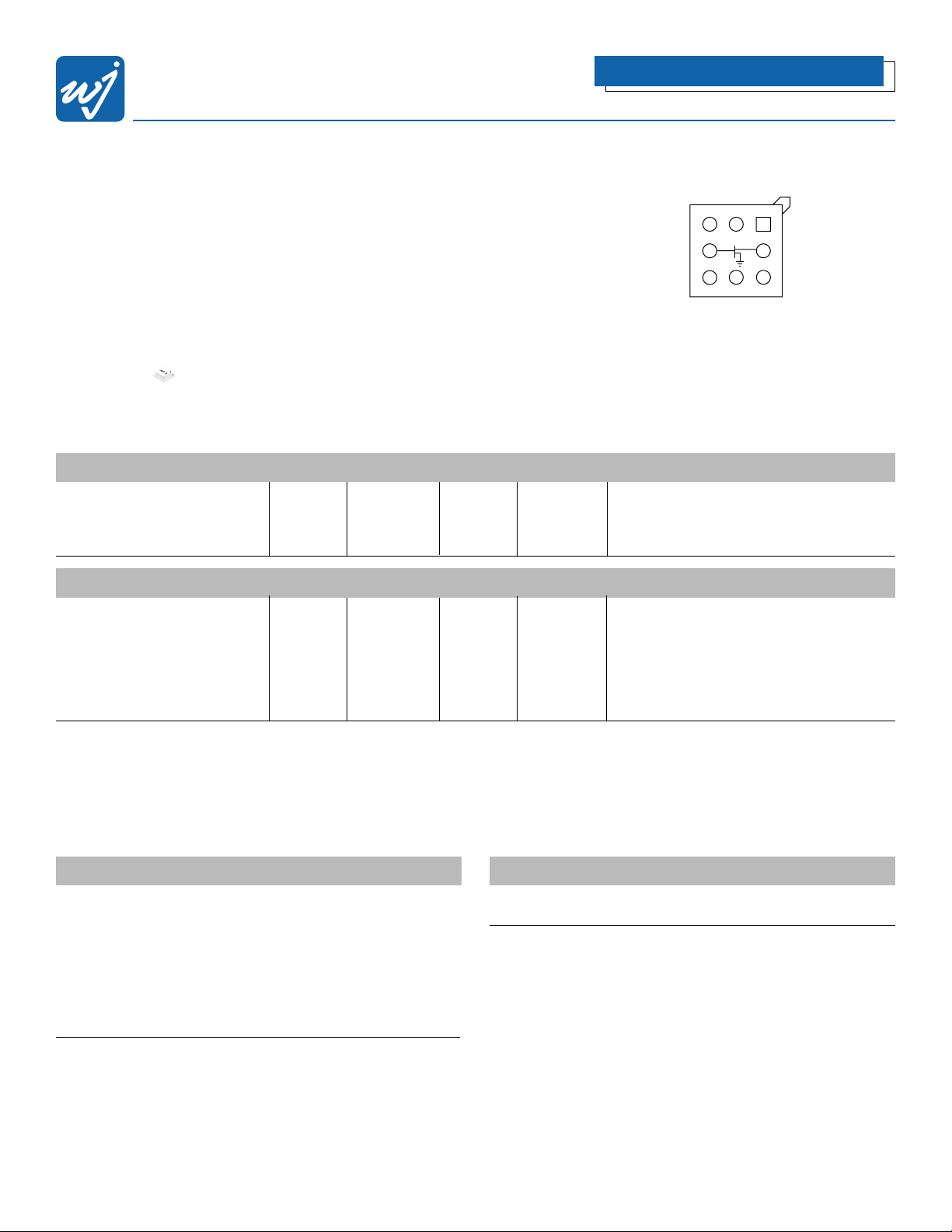
Functional Diagram
High Dynamic Range FET
Specifications
DC Electrical Parameter Units Minimum Typical Maximum Condition
Saturated Drain Current, Idss mA 220 340 380 Vgs = 0V
Transconductance, Gm mS 120
Pinch Off Voltage, Vp V -5.0 -3.7 Ids = 1.2 mA
RF Parameter Units Minimum Typical Maximum Condition
Small Signal Gain, Gss dB 13 15
Maximum Stable Gain, Gmsg dB 22.5
Output IP3 dBm 36 39
Output P1dB dBm 23.5 25
Noise Figure, NF dB 2
Notes:
1. DC and RF parameters measured under the following conditions unless otherwise noted.
22°C with Vds = 8.0 volts, Ids = 100 mA, Test frequency = 800 MHz, 50 Ω system.
2. Idss is measured with Vgs = 0 V.
3. Pinch off voltage is measured when Ids = 0.6 mA.
4. MTBF calculated with channel temperature at 155˚C.
Absolute Maximum Ratings
Parameter Rating
Drain to Source Voltage 9 V
Gate to Source Voltage -6.0 V
Operating Case Temperature -40 to +80 °C
Storage Temperature -55 to +125°C
Input RF Power (continuous) +12 dBm
Gate Current 6 mA
Maximum DC Power 0.9 W
Operation of this device above any of these parameters may cause per manent damage.
Ordering Information
Part No. Description
AP3 High Dynamic Range FET
(Available in tape and reel)
TOP VIEW
The Communications Edge
™
Advanced Product Information
Actual Size
Pin 1 indicator
Gate
(Neg bias)
All other pins including
center pin are grounded
Drain
(Pos bias)
Page 2
WJ Communications, Inc. • Phone: 1-800-WJ1-4401 • FAX:408-577-6620 • e-mail:sales@wj.com • Web site: www.wj.com
February 2002
AP3
Advanced Product Information
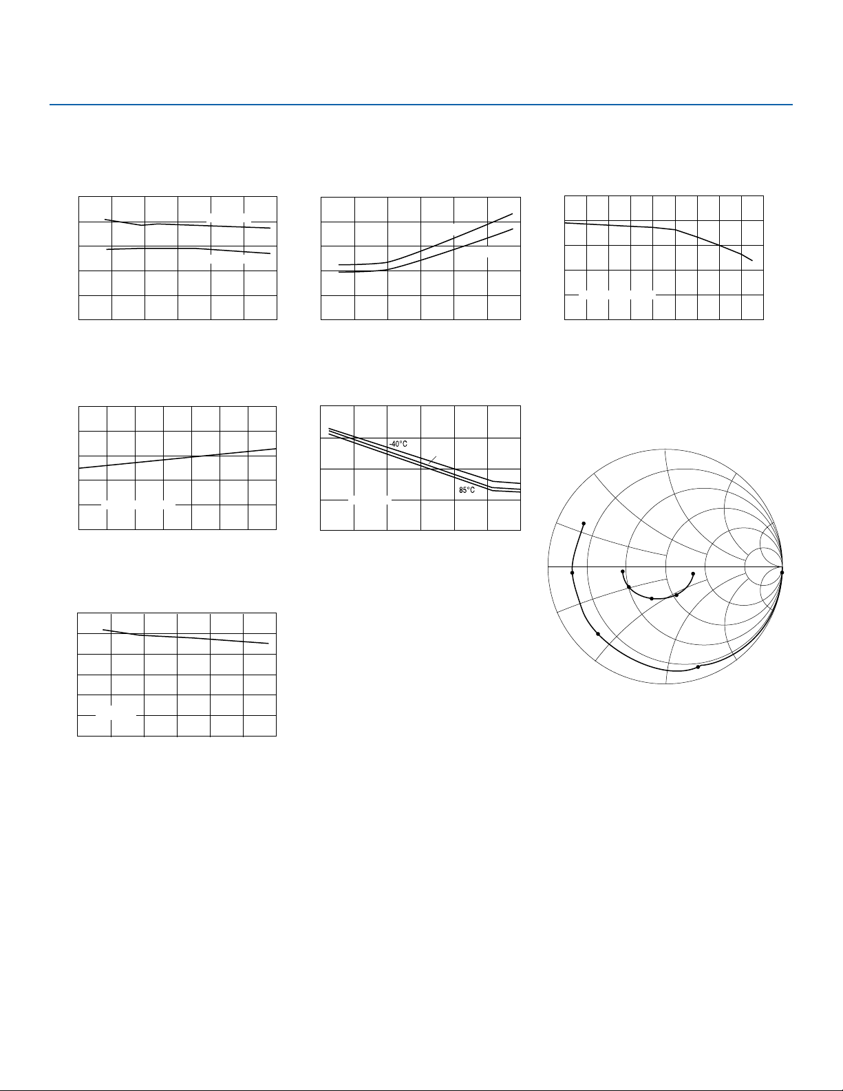
Performance Charts (Vds = 8 V, Ids = 100 mA, T = 22°C, unmatched 50 ohm system) unless noted
OIP3 vs. Frequency
45
40
35
30
OIP3 (dBm)
25
20
01234 65
Frequency (GHz)
8 V, 100 mA
5 V, 100 mA
OIP3 vs. Temperature
50
45
40
35
OIP3 (dBm)
8 V, 100 mA, 800 MHz
30
25
-40 -20 0 20 40 60 10080
Temperature (C)
P1dB vs. Frequency
30
25
20
15
P1dB (dBm)
10
8 V, 100 mA
5
0
01234 65
Frequency (GHz)
Noise Figure vs. Frequency
5
4
3
2
Noise Figure (dB)
1
0
0123456
8 V, 100 mA
5 V, 100 mA
Frequency (GHz)
45
40
35
30
OIP3 (dBm)
8 V, 100 mA, 800 MHz
25
20
02468 1210 14 1816
Gain vs. Frequency over Temperature
20
15
Room
10
Gain (dB)
5
8 V, 100 mA
S11
0
0231456
Frequency (GHz)
6.0
4.5
3.0
OIP3 vs. Power Out
Output Power (dBm)
S-Parameters
S22
1.5
Frequency (GHz)
Start 0.1; Stop 6.0
0.1
Page 3

WJ Communications, Inc. • Phone: 1-800-WJ1-4401 • FAX:408-577-6620 • e-mail:sales@wj.com • Web site: www.wj.com
February 2002
AP3
Advanced Product Information
Outline Drawing
This document contains information on a new product.
Specifications and information are subject to change without notice.
Caution! ESD sensitive device.
Land Pattern
Mounting Configuration
Page 4

WJ Communications, Inc. • Phone: 1-800-WJ1-4401 • FAX:408-577-6620 • e-mail:sales@wj.com • Web site: www.wj.com
February 2002
AP3
T ypical Test Data
S-Parameters (Vds = 5 V, Ids = 100 mA,T = 22°C, unmatched device in a 50 ohm system)
Freq (GHz) S11 (Mag) S11 (Ang) S21 (Mag) S21 (Ang) S12 (Mag) S12 (Ang) S22 (Mag) S22 (Ang) K Value
0.1 0.99965 -6.50407 6.44820 172.363 0.00380 79.4633 0.16645 -9.02007 0.0338
0.5 0.97741 -30.3703 6.00960 143.029 0.01908 57.0606 0.17642 -38.6303 0.2499
1.0 0.93840 -51.4107 5.39510 111.092 0.03281 28.1409 0.19838 -61.7507 0.4688
1.5 0.90982 -74.9390 5.22060 72.9401 0.04667 -5.67977 0.18747 -92.2131 0.5621
2.0 0.87125 -100.670 4.71260 38.6735 0.05538 -35.4865 0.24343 -116.930 0.7253
2.5 0.83724 -121.380 4.08080 7.94187 0.05966 -62.7289 0.30376 -126.030 0.9274
3.0 0.81879 -134.090 3.67820 -19.6747 0.06451 -87.2985 0.31343 -130.290 0.9819
3.5 0.80262 -147.010 3.41240 -48.0444 0.07048 -111.269 0.28259 -143.110 0.9491
4.0 0.79049 -163.730 3.04350 -77.1640 0.06845 -139.450 0.28898 -161.400 1.0019
4.5 0.80381 -177.160 2.62769 -104.632 0.06470 -158.872 0.35652 -164.760 0.9360
5.0 0.79493 176.260 2.37730 -128.416 0.06261 -177.019 0.38736 -160.340 0.8849
5.5 0.77739 170.650 2.36900 -152.963 0.06648 166.323 0.33766 -161.460 0.9299
6.0 0.77053 157.220 2.30970 178.884 0.06938 145.067 0.29808 -179.171 1.0124
S-Parameters (Vds = 8 V, Ids = 100 mA,T = 22°C, unmatched device in a 50 ohm system)
Freq (GHz) S11 (Mag) S11 (Ang) S21 (Mag) S21 (Ang) S12 (Mag) S12 (Ang) S22 (Mag) S22 (Ang) K Value
0.1 0.99997 -6.50607 6.13330 172.243 0.00420 82.9643 0.26433 -6.39707 0.0227
0.5 0.97747 -30.3603 5.71250 142.645 0.01878 56.6910 0.26392 -27.9603 0.3020
1.0 0.93820 -51.3707 5.11860 110.330 0.03311 28.3369 0.27280 -47.0407 0.5509
1.5 0.90978 -74.7510 4.97080 72.2901 0.04651 -6.17482 0.24395 -70.7840 0.6550
2.0 0.87271 -100.450 4.49270 37.5335 0.05442 -36.3184 0.27286 -96.3961 0.7998
2.5 0.83960 -120.960 3.88590 6.32887 0.05895 -64.3282 0.32398 -109.200 0.9605
3.0 0.82069 -133.800 3.49200 -21.5137 0.06254 -88.1869 0.33718 -114.270 0.9785
3.5 0.80499 -146.770 3.24230 -49.8954 0.06791 -113.262 0.30385 -124.920 0.9134
4.0 0.79343 -163.340 2.89680 -79.2840 0.06684 -140.253 0.29517 -142.450 0.9134
4.5 0.80655 -176.850 2.49519 -107.370 0.06142 -160.677 0.36664 -150.130 0.9548
5.0 0.80028 176.550 2.24440 -131.481 0.05933 -177.572 0.41133 -147.830 0.9109
5.5 0.78276 170.820 2.23290 -155.797 0.06176 164.915 0.37316 -147.530 0.9944
6.0 0.77528 157.310 2.18810 176.064 0.06490 145.070 0.32381 -162.310 1.1199
Advanced Product Information
 Loading...