

Page 1
A
V
Green
SINGLE SLEW RATE CONTROLLED LOAD SWITCH
Description
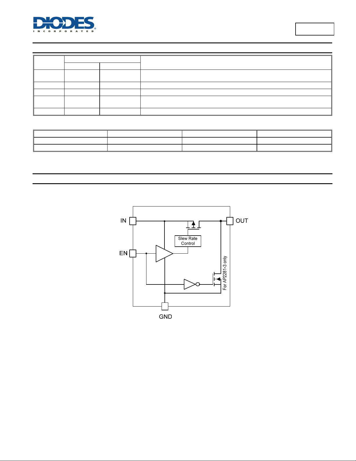
The AP2281 slew rate controlled load switch is a single P-channel
MOSFET power switch designed for high-side load-switching
applications. The MOSFET has a typical R
allowing increased load current handling capacity with a low forward
voltage drop. The turn-on slew rate of the device is controlled
internally.
The AP2281 load switch is designed to operate from 1.5V to 6V,
making it ideal for 1.8V, 2.5V, 3.3V, and 5V systems. The typical
quiescent supply current is only 0.01µA.
of 80m at 5V,
DS(ON)
Features
Wide input voltage range: 1.5V – 6V
Low R
Turn-on slew rate controlled
AP2281-1: 1ms turn-on rise time
AP2281-3: 100µs turn-on rise time with internal discharge
Very low turn-on quiescent current: << 1µA
Fast load discharge option
Temperature range -40°C to +85°C
Lead-Free Finish; RoHS Compliant (Notes 1 & 2)
Halogen and Antimony Free. “Green” Device (Note 3)
: 80mΩ typical @ 5V
DS(ON)
Applications
Smart Phones
PDA
Cell Phones
GPS Navigators
PMP/MP4
Notebook and Pocket PC
Notes: 1. EU Directive 2002/95/EC (RoHS) & 2011/65/EU (RoHS 2) compliant. All applicable RoHS exemptions applied.
2. See http://www.diodes.com/quality/lead_free.html for more information about Diodes Incorporated’s definitions of Halogen- and Antimony-free, "Green"
and Lead-free.
3. Halogen- and Antimony-free "Green” products are defined as those which contain <900ppm bromine, <900ppm chlorine (<1500ppm total Br + Cl) and
<1000ppm antimony compounds.
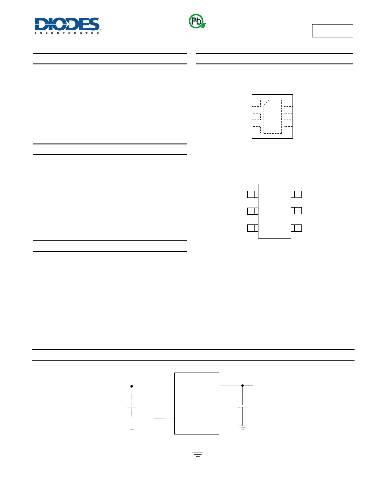
Pin Assignments
OUT
GND
EN IN
( Top View )
1
IN
2
IN
3
EN
U-DFN2018-6
1
2
7
(Top View)
SOT26
6
OUT
5
OUT
4
GND
IN
6
GND
5
43
P2281
Typical Applications Circuit
AP2281
Document number: DS31359 Rev. 7 - 2
IN
1uF
IN
Enable
EN
OUT
GND
OUT
V
0.1uF
1 of 11
www.diodes.com
November 2013
© Diodes Incorporated
Page 2
A
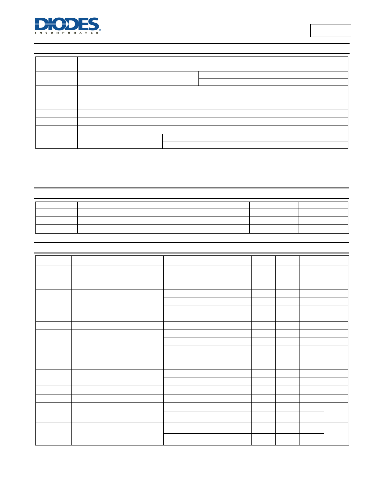
Pin Descriptions
P2281
Pin Name
OUT
GND 2, 5 4 Ground.
EN 3 3 Enable input, active high
IN
PAD 7 Thermal pad. Suggest connecting to ground plane to get better heat dissipation.
Pin Number
SOT26 U-DFN2018-6
1 5, 6
4, 6 1, 2
Voltage output pin. This is the pin to the P-channel MOSFET drain connection. Bypass to ground
through a 0.1uF capacitor.
Voltage input pin. This is the pin to the P-channel MOSFET source. Bypass to ground through a
1µF capacitor.
Function
Options
Part Number Slew Rate (typ) Active Pull Down Enable
AP2281-1 1ms No Active High
AP2281-3 100µs Yes Active High
Functional Block Diagram
AP2281
Document number: DS31359 Rev. 7 - 2
2 of 11
www.diodes.com
November 2013
© Diodes Incorporated
Page 3
A
P2281
Absolute Maximum Ratings (@T
= +25°C, unless otherwise specified.)
A
Symbol Parameter Ratings Unit
ESD HBM Human Body Model ESD Protection 5 KV
ESD MM Machine Model ESD Protection
V
IN
V
OUT
V
EN
I
load
T
J
T
ST
P
D
Notes: 4. TJ, max = +125°C.
5. Ratings apply to ambient temperature at +25°C.
Stresses greater than the 'Absolute Maximum Ratings' specified above, may cause permanent damage to the device. These are stress ratings only; functional
operation of the device at these or any other conditions exceeding those indicated in this specification is not implied. Device reliability may be affected by exposure to
absolute maximum rating conditions for extended periods of time.
Input Voltage 6.5 V
Output Voltage VIN +0.3 V
Enable Voltage 6.5 V
Maximum Continuous Load Current 2 A
Operating Junction Temperature Range -40 to +125 °C
Storage Temperature Range -65 to +150 °C
Power Dissipation
SOT26 (Note 4, 5, 6) 720 mW
U-DFN2018-6 (Note 4, 5, 7) 1410 mW
SOT26 500 V
U-DFN2018-6 450 V
Recommended Operating Conditions (@T
= +25°C, unless otherwise specified.)
A
Symbol Parameter Min Max Unit
V
I
OUT
T
IN
A
Input voltage 1.5 6.0 V
Output Current 0 2.0 A
Operating Ambient Temperature -40 +85 °C
Electrical Characteristics (@T
= +25°C, unless otherwise specified.)
A
Symbol Parameters Test Conditions Min Typ Max Unit
I
SHDN
I
LEAK
R
DS(ON)
V
V
I
SINK
T
D(ON)
T
T
D(OFF)
R
DISCH
θJA
θJC
I
ON
Q
Input Quiescent Current
Input Shutdown Current
Input Leakage Current
Switch on-resistance
V
= VIN, I
EN
V
= 0V, OUT open
EN
V
= 0V, OUT grounded
EN
= 5.0V
V
IN
OUT
= 0
VIN = 3.3V
VIN = 1.8V
VIN = 1.5V
IL
IH
EN Input Logic Low Voltage
EN Input Logic High Voltage
EN Input leakage
Output turn-on delay time
Output turn-on rise time
Output turn-off delay time
Discharge FET on-resistance
V
= 1.5V to 6V
IN
1.5V ≤ V
≤ 2.7V
IN
2.7V < VIN < 5.25V
V
≥ 5.25V
IN
V
= 5V
EN
R
= 10Ω
LOAD
AP2281-1, R
AP2281-3, R
R
= 10Ω
LOAD
LOAD
LOAD
= 10Ω
= 10Ω
For AP2281-3 only, V
= GND
EN
SOT26 (Note 6)
Thermal Resistance Junction-to-Ambient
U-DFN2018-6 (Note 7)
SOT26 (Note 6)
Thermal Resistance Junction-to-case
U-DFN2018-6 (Note 7)
— 0.01 1 μA
—
—
—
—
—
—
— —
1.4
1.6
1.7
— —
—
—
—
—
—
—
—
—
—
0.01 1 μA
0.01 1 μA
80 100 mΩ
95 120
160 210
mΩ
mΩ
210 280 mΩ
0.4 V
— —
— —
— —
1 μA
1 — μS
1000 1500 μS
100 150 μS
0.5 1 μS
65 100 Ω
153
78
29
19
—
—
—
—
°C/W
°C/W
V
V
V
Notes: 6. Test condition for SOT26: Device mounted on FR-4 substrate PC board, 2oz copper, with minimum recommended pad layout.
7. Test condition for U-DFN2018-6: Device mounted on FR-4 2-layer board, 2oz copper, with minimum recommended pad on top layer and 3 vias to bottom
layer 1.0"x1.4" ground plane.
AP2281
Document number: DS31359 Rev. 7 - 2
3 of 11
www.diodes.com
November 2013
© Diodes Incorporated
Page 4
A
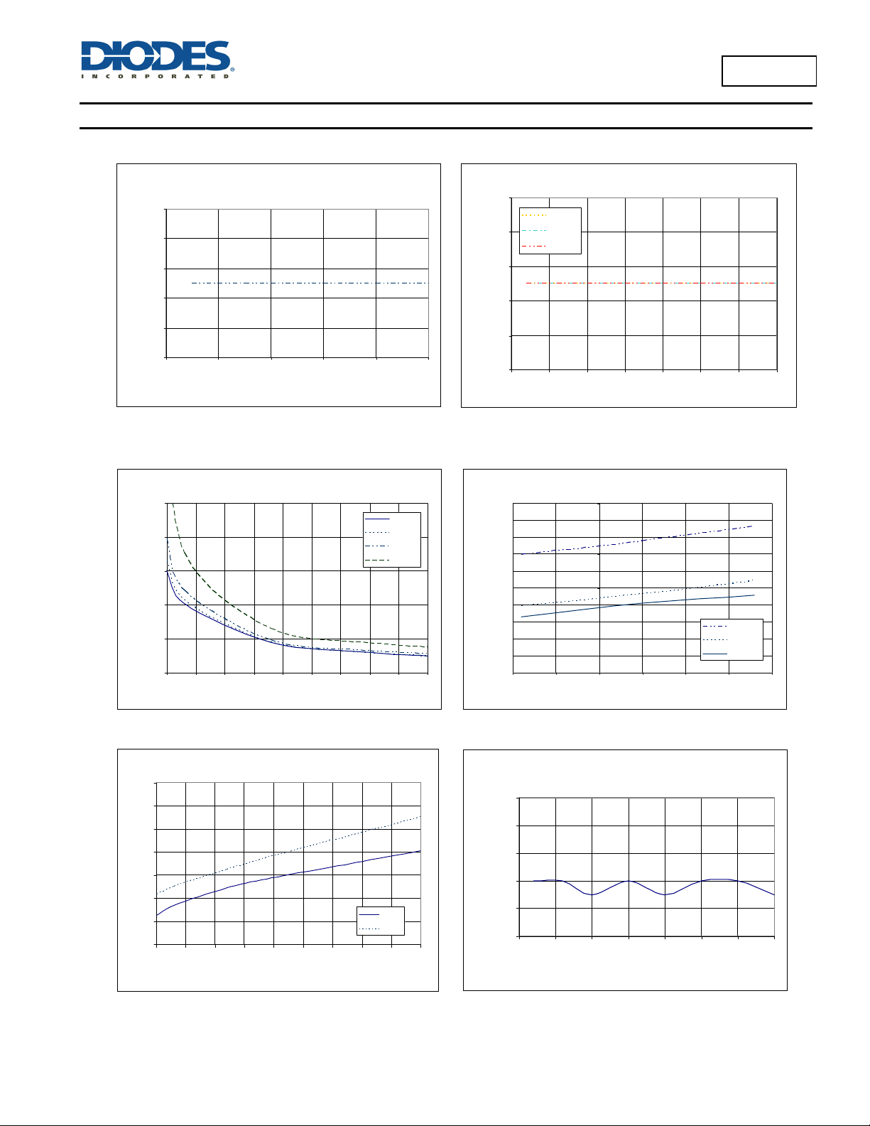
Typical Performance Characteristics
P2281
Quiescent Current vs. Input Voltage
0.01
A)
0.008
0.006
0.004
0.002
Quiescent Current (
0
1.02.0 3.04.0 5.06.0
Inpu t Voltage (V)
R
vs. Input Voltage
DS( ON)
I=100mA
I=500mA
I=1A
I=2A
)
300.00
250.00
200.00
(m
150.00
DS(ON)
R
100.00
50.00
1.522.533.544.555.56
Input Voltage (V)
Quiescent Current vs. Temperature
0.010
A)
0.008
0.006
0.004
0.002
VIN=1.8V
VIN=3.3V
VIN=5.0V
Quiescent Current (
0.000
-50 -25 0 25 50 75 100 125
Temperature (°C)
R
vs. Temperature
DS( ON)
200.00
180.00
160.00
140.00
)
120.00
(m
100.00
80.00
DS(ON)
R
60.00
40.00
20.00
0.00
-50 -25 0 25 50 75 100
Temperature (°C)
VIN =1.8V
VIN =3.3V
VIN =5V
ENABLE Threshold vs. Input Voltage
1.8
1.6
1.4
1.2
1.0
0.8
ON/OFF Threshold (V)
0.6
0.4
1.5 2.0 2.5 3.0 3.5 4.0 4.5 5.0 5.5 6.0
AP2281
Document number: DS31359 Rev. 7 - 2
Input Voltage (V )
VIL (V)
VIH (V)
4 of 11
www.diodes.com
Input Shutdown Current vs. Temperature
0.010
0.008
A)
0.006
(
0.004
SHDN
I
0.002
0.000
-50 -25 0 25 50 75 100 125
Temperature (°C)
November 2013
© Diodes Incorporated
Page 5

A
Typical Performance Characteristics (cont.)
AP2281-1 Turn-On
= 3.3V, RL = 7Ω)
(V
IN
AP2281-1 Turn-Off
(V
= 3.3V, RL = 7Ω)
IN
P2281
V
(5V/div)
EN
V
(2V/div)
OUT
I
(500mA/div)
IN
Time (500μs/div)
VEN (5V/div)
V
OUT
IIN (500mA/div)
(2V/div)
Time (50μs/div)
V
V
EN
OUT
(5V/div)
(2V/div)
AP2281-1 Turn-On
(V
= 5V, RL = 10Ω)
IN
VEN (5V/div)
V
(2V/div)
OUT
AP2281-1 Turn-Off
(V
= 5V, RL = 10Ω)
IN
I
(500mA/div)
IN
Time (500μs/div)
AP2281-3 Turn-On
= 3.3V, RL = 7Ω)
(V
IN
VEN (5V/div)
V
OUT
I
IN
(2V/div)
(500mA/div)
Time (50μs/div)
AP2281
Document number: DS31359 Rev. 7 - 2
IIN (500mA/div)
Time (50μs/div)
AP2281-3 Turn-Off
= 3.3V, RL= 7Ω)
(V
IN
VEN (5V/div)
V
(2V/div)
OUT
IIN (500mA/div)
5 of 11
www.diodes.com
Time (50μs/div)
November 2013
© Diodes Incorporated
Page 6

A
Typical Performance Characteristics (cont.)
P2281
AP2281-3 Turn-Off
(V
= 5V, RL=10Ω)
IN
Time (50μs/div)
V
(5V/div)
EN
V
(2V/div)
OUT
I
(500mA/div)
IN
AP2281-3 Turn-On
= 5V, RL = 10Ω)
(V
IN
Time (50μs/div)
VEN (5V/div)
V
OUT
IIN (500mA/div)
(2V/div)
Application Notes
Input Capacitor
A 1μF capacitor is recommended to connect between IN and GND pins to decouple input power supply glitch and noise. The input capacitor has
no specific type or ESR (Equivalent Series Resistance) requirement. However, for higher current application, ceramic capacitors are
recommended due to their capability to withstand input current surges from low impedance sources, such as batteries in portable applications.
This input capacitor must be located as close as possible to the device to assure input stability and less noise. For PCB layout, a wide copper
trace is required for both IN and GND
.
Output Capacitor
A 0.1μF capacitor is recommended to connect between OUT and GND pins to stabilize and accommodate load transient condition. The output
capacitor has no specific type or ESR requirement. The amount of the capacitance may be increased without limit. For PCB layout, the output
capacitor must be placed as close as possible to OUT and GND pins, and keep the traces as short as possible.
ENABLE/SHUTDOWN Operation
The AP2281 is turned on by setting the EN pin high, and is turned off by pulling it low. To ensure proper operation, the signal source used to
drive the EN pin must be able to swing above and below the specified turn-on/off voltage thresholds listed in the Electrical Characteristics section
under V
and VIH.
IL
DISCHARGE Operation
The AP2281-3 offers discharge option that helps to discharge the output charge when disabled.
Power Dissipation
The device power dissipation and proper sizing of the thermal plane is critical to avoid thermal shutdown and ensure reliable operation. Power
dissipation of the device depends on input voltage and load conditions and can be calculated by:
2
xRIP
OUTD
(1)
DSON
However, the maximum power dissipation that can be handled by the device depends on the maximum junction to ambient thermal resistance,
maximum ambient temperature, and maximum device junction temperature, which can be approximated by the equation below:
)TC125(
)T(max@P
(2)
AD
For example at V
Based on SOT26 θ
= 5V, the typical R
IN
= 153°C/W and equation (2), the calculated junction temperature rise from ambient is approximately 49°C. Since the
JA
= 80mΩ. For I
DSON
= 2A, the maximum power dissipation calculated using equation (1) is PD = 0.32W.
OUT
maximum junction temperature is 125°C, the operating ambient temperature must be kept below 76°C to safely operate the device.
AP2281
Document number: DS31359 Rev. 7 - 2
6 of 11
www.diodes.com
A
JA
November 2013
© Diodes Incorporated
Page 7

A
Application Notes (cont.)
P2281
On the other hand, at T
Hence the safe operating maximum continuous current is 1.81A. For other application conditions, the users should recalculate the device
maximum power dissipation based on the operating conditions.
= +85°C and V
A
= 5V, the calculated maximum power dissipation from equation (2) is approximately P
IN
D(MAX)
= 0.26W.
Ordering Information
AP2281 - X XX G -7
Turn-on rise time
1 : 1ms
3 : 100us
Package
W : SOT26
FM : U-DFN2018-6
Green
G : Green
Packing
7 : Tape & Reel
Part Number Package Code Packaging
AP2281-1WG-7 W SOT26 3000/Tape & Reel -7
AP2281-3WG-7 W SOT26 3000/Tape & Reel -7
AP2281-1FMG-7 FM U-DFN2018-6 3000/Tape & Reel -7
AP2281-3FMG-7 FM U-DFN2018-6 3000/Tape & Reel -7
Quantity Part Number Suffix
7” Tape and Reel
Marking Information
(1) SOT26
( Top View )
(2) U-DFN2018-6
6
XX Y
1 2 3
Device Package Type Identification Code
AP2281-1W SOT26 U2
AP2281-3W SOT26 U3
WX
4
XX : Identification code
: Year 0~9
Y
: Week : A~Z : 1~26 week;
W
a~z : 27~52 week; z represents
52 and 53 week
: A~Z : Green
X
7
5
( Top View )
XX : Identification code
Y
XX
Y
W X
.
: Year 0~9
: Week : A~Z : 1~26 week;
W
a~z : 27~52 week; z represents
52 and 53 week
: A~Z : Green
X
Device Package Type Identification Code
AP2281-1FM U-DFN2018-6 UE
AP2281-3FM U-DFN2018-6 UF
AP2281
Document number: DS31359 Rev. 7 - 2
7 of 11
www.diodes.com
November 2013
© Diodes Incorporated
Page 8

A
Package Outline Dimensions (All dimensions in mm.)
Please see AP02002 at http://www.diodes.com/datasheets/ap02002.pdf for latest version.
(1) SOT26
(2) U-DFN2018-6
K
J
A
Dim Min Max Typ
A 0.35 0.50 0.38
B C
H
M
D
L
B 1.50 1.70 1.60
C 2.70 3.00 2.80
D
H 2.90 3.10 3.00
J 0.013 0.10 0.05
K 1.00 1.30 1.10
L 0.35 0.55 0.40
M 0.10 0.20 0.15
All Dimensions in mm
Dim Min Max Typ
A 0.545 0.605 0.575
A1 0 0.05 0.02
A3
b 0.15 0.25 0.20
D 1.750 1.875 1.80
D2 1.30 1.50 1.40
e
E 1.95 2.075 2.00
E2 0.90 1.10 1.00
L 0.20 0.30 0.25
z
All Dimensions in mm
SOT26
0° 8°
U-DFN2018-6
P2281
0.95
0.13
0.50
0.30
AP2281
Document number: DS31359 Rev. 7 - 2
8 of 11
www.diodes.com
November 2013
© Diodes Incorporated
Page 9

A
Suggested Pad Layout
Please see AP02001 at http://www.diodes.com/datasheets/ap02001.pdf for the latest version.
(1) SOT26
(2) U-DFN2018-6
Y
Y1
AP2281
Document number: DS31359 Rev. 7 - 2
G
Z
Y
X
XC
X1
C2
C2
G
www.diodes.com
C1
Dimensions Value (in mm)
Z
G
X
Y
C1 2.40
C2
Dimensions Value (in mm)
C 0.50
G 0.20
X 0.25
X1 1.60
Y 0.35
Y1 1.20
9 of 11
3.20
1.60
0.55
0.80
0.95
P2281
November 2013
© Diodes Incorporated
Page 10

A
Taping Orientation
P2281
Note: 8. The taping orientation of the other package type can be found on our website at http://www.diodes.com/datasheets/ap02007.pdf
AP2281
Document number: DS31359 Rev. 7 - 2
10 of 11
www.diodes.com
November 2013
© Diodes Incorporated
Page 11

A
P2281
DIODES INCORPORATED MAKES NO WARRANTY OF ANY KIND, EXPRESS OR IMPLIED, WITH REGARDS TO THIS DOCUMENT,
INCLUDING, BUT NOT LIMITED TO, THE IMPLIED WARRANTIES OF MERCHANTABILITY AND FITNESS FOR A PARTICULAR PURPOSE
(AND THEIR EQUIVALENTS UNDER THE LAWS OF ANY JURISDICTION).
Diodes Incorporated and its subsidiaries reserve the right to make modifications, enhancements, improvements, corrections or other changes
without further notice to this document and any product described herein. Diodes Incorporated does not assume any liability arising out of the
application or use of this document or any product described herein; neither does Diodes Incorporated convey any license under its patent or
trademark rights, nor the rights of others. Any Customer or user of this document or products described herein in such applications shall assume
all risks of such use and will agree to hold Diodes Incorporated and all the companies whose products are represented on Diodes Incorporated
website, harmless against all damages.
Diodes Incorporated does not warrant or accept any liability whatsoever in respect of any products purchased through unauthorized sales channel.
Should Customers purchase or use Diodes Incorporated products for any unintended or unauthorized application, Customers shall indemnify and
hold Diodes Incorporated and its representatives harmless against all claims, damages, expenses, and attorney fees arising out of, directly or
indirectly, any claim of personal injury or death associated with such unintended or unauthorized application.
Products described herein may be covered by one or more United States, international or foreign patents pending. Product names and markings
noted herein may also be covered by one or more United States, international or foreign trademarks.
This document is written in English but may be translated into multiple languages for reference. Only the English version of this document is the
final and determinative format released by Diodes Incorporated.
Diodes Incorporated products are specifically not authorized for use as critical components in life support devices or systems without the express
written approval of the Chief Executive Officer of Diodes Incorporated. As used herein:
A. Life support devices or systems are devices or systems which:
1. are intended to implant into the body, or
2. support or sustain life and whose failure to perform when properly used in accordance with instructions for use provided in the
labeling can be reasonably expected to result in significant injury to the user.
B. A critical component is any component in a life support device or system whose failure to perform can be reasonably expected to cause the
failure of the life support device or to affect its safety or effectiveness.
Customers represent that they have all necessary expertise in the safety and regulatory ramifications of their life support devices or systems, and
acknowledge and agree that they are solely responsible for all legal, regulatory and safety-related requirements concerning their products and any
use of Diodes Incorporated products in such safety-critical, life support devices or systems, notwithstanding any devices- or systems-related
information or support that may be provided by Diodes Incorporated. Further, Customers must fully indemnify Diodes Incorporated and its
representatives against any damages arising out of the use of Diodes Incorporated products in such safety-critical, life support devices or systems.
Copyright © 2013, Diodes Incorporated
www.diodes.com
IMPORTANT NOTICE
LIFE SUPPORT
AP2281
Document number: DS31359 Rev. 7 - 2
11 of 11
www.diodes.com
November 2013
© Diodes Incorporated
Page 12

 Loading...