

Datasheet AP131-15W, AP131-18W, AP131-20W, AP131-25W, AP131-28W Datasheet (Diodes) [ru]
...Page 1
AP131
300mA LOW DROPOUT LINEAR REGULATOR WITH
SHUTDOWN
Features
• Input Voltage Range is from 2.7 to 5.5V
• Dropout Voltage 400mV at 300mA Output Current
• Guaranteed 300mA Output Current
• Internal Ron = 1.5Ω PMOS draws no Base Current
• Low Quiescent Current 50µA
• Output Voltage: 1.5V/1.8V/2.0V/2.5V/2.8V/
• 2.9V/3.0V/3.3V/ 3.5V; Accuracy 2%
• Active Low Shutdown Function (EN pin)
• Fast Transient Response
• Good Load Regulation
• Current Limit and Thermal Shutdown Protection
• Short Circuit Current Fold-Back
• Lead Free package: SOT25
• SOT25: Available in “Green” Molding Compound
(No Br, Sb)
• Lead Free Finish/RoHS Compliant (Note 1)
Applications
• Battery Powered Device
• Wireless Communication
• CD-ROM, DVD, and LAN Card
• PC Peripheral
Ordering Information
AP131 - XX W X - 7
General Description
The AP131 is a 300mA, fixed output voltage, low dr opout linear
regulator. The Device included pass element, error amplifier,
band-gap, current limit and thermal shutdown circuitry. The
device is ON when the EN pin is set to logic high level.
The characteristics of low dropout voltage and less quiescent
current make it good for some critical current applications, for
example, some battery powered devices. The typical quiescent
current is approximately 50µA from zero to maximum load. Due
to the internal flexible design, it results in extensively fixed output
voltage versions and makes it convenient to use for applications.
Built-in current-limit and thermal-shutdown functions prevent any
fault condition from IC damage. An external capacitor can be
connected to the BP pin and reduce the output noise.
Output Voltage
15 :1.5V
18 :1.8V
Package Packing
W : SOT25
Lead Free
L : Lead Free
G : Green
7 : Tape & Reel
20 :2.0V
25 :2.5V
28 :2.8V
29 :2.9V
30 :3.0V
33 :3.3V
35 :3.5V
Device
AP131-XXWL-7
Lead-free
AP131-XXWG-7
Notes: 1. EU Directive 2002/95/EC (RoHS). All applicable RoHS exemptions applied. Please visit our website at
http://www.diodes.com/products/lead_free.html
2. Pad layout as shown on Diodes Inc. suggested pad layout document AP02001, which can be found on our website at
http://www.diodes.com/datasheets/ap02001.pdf
Package
Code
W SOT25
W SOT25
Packaging
(Note 2)
.
.
Quantity Part Number Suffix
3000/Tape & Reel -7
3000/Tape & Reel -7
7” Tape and Reel
AP131 Rev. 7 1 of 7 FEBRUARY 2009
www.diodes.com © Diodes Incorporated
Page 2
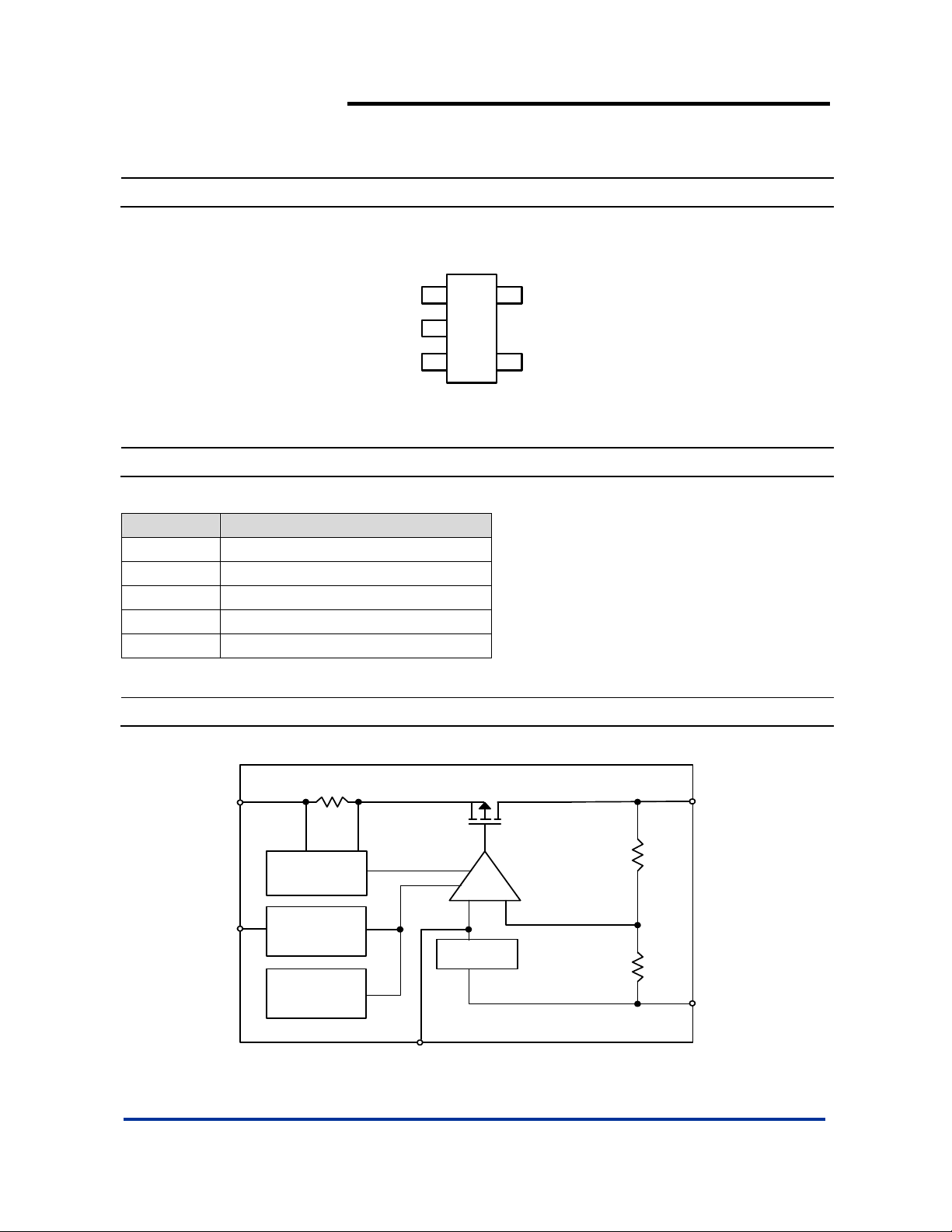
Pin Assignment
AP131
300mA LOW DROPOUT LINEAR REGULATOR WITH
SHUTDOWN
( Top View )
Pin Description
Pin Name Description
IN Input Voltage
GND Ground
EN Enable Pin
BP Band-gap
OUT Output Voltage
Block Diagram
1IN
OUT
5
2
3
EN BP
4
SOT25
IN
EN
Current
Limit
Enable
-
+
Bandgap
Error
Amp
1.08V
OUT
Thermal
Shutdown
BP
AP131 Rev. 7 2 of 7 FEBRUARY 2009
www.diodes.com © Diodes Incorporated
GND
Page 3
AP131
300mA LOW DROPOUT LINEAR REGULATOR WITH
SHUTDOWN
Absolute Maximum Ratings
Symbol Parameter Rating Unit
VCC Input Voltage +6 V
TOP Operating Junction Temperature Range -40 to +125 ºC
TST Storage Temperature Range -65 to +150 ºC
PD Power Dissipation, PD @ TA = 25ºC SOT25 250 mW
Recommended Operating Conditions
Symbol Parameter Min Max Unit
V
IN
I
OUT
T
A
AP131 Rev. 7 3 of 7 FEBRUARY 2009
Input Voltage 2.7 5.5 V
Output Current 0 300 mA
Operating Ambient Temperature -40 85
www.diodes.com © Diodes Incorporated
°C
Page 4

AP131
300mA LOW DROPOUT LINEAR REGULATOR WITH
SHUTDOWN
Electrical Characteristics
T
= 25ºC, C
A
Symbol Parameter Conditions Min Typ. Max Unit
V
DROP
I
LIMIT
I
short
ΔV
ΔV
ΔV
PSRR Ripple Rejection
ISB Standby Current IL = 0mA, V
IQ Quiescent Current IL = 0mA, V
IEN Enable Pin Current - - < 0. 1 μA
V
ENON
V
ENOFF
T
DELAY
θ
θ
Notes: 3. Dropout voltage is defined as the input to output differential voltage. Dropout is measured at constant junction temperature by using pulsed ON
time, and the criterion is V
4. Current limit is measured at constant junction temperature by using pulsed testing with a low ON time.
5. Regulation is measured at constant junction temperature by using pulsed testing with a low ON time.
6. Guaranteed by design.
7. Test conditions for SOT25: Device mounted on FR-4 substrate PC board, 2oz copper, with minimum recommended pad layout.
= 1µF, C
IN
= 10µF, unless otherwise specified.
OUT
Dropout Voltage (Note 3) IL = 300mA - 400 500 mV
Current Limit (Note 4) V
Short Circuit Current V
Line Regulation
LINE
Load Regulation (Note 5) IL = 1~300mA, V
LOAD
Output Voltage Accuracy I
OUT
Output Voltage Temperature
Coefficient (Note 6)
= 5V, V
IN
< 1.05V - 150 300 mA
OUT
I
=1mA, V
OUT
to 5.5V
= 1mA, V
L
= 0V 350 450 - mA
OUT
IN =( VOUT
= 5V -2 - +2 %
IN
+1V )
= 5V - 30 35 mV
IN
- 0.1 0.3 %/V
- 50 150
PPM/
ºC
F = 100Hz,
C
= 1μF, CO = 10uF,
IN
I
= 100mA
L
= 5V, EN = 0V - - 5 μA
IN
= 5V, EN = 5V - 50 100 μA
IN
Enable Pin Voltage
Output OFF 0 - 0.8 V
Enable Delay Time
Thermal Resistance
JA
JC
Junction-to-Ambient
Thermal Resistance
Junction-to-Case
inside target value ±2%. This test is skipped at the condition of VIN<3V.
OUT
Output ON 1.5 - VIN V
= 0.1μF, C
C
BP
= 30mA
I
OUT
OUT
= 1μF,
SOT25 (Note 7) 163
SOT25 (Note 7) 53
- 60 - dB
- 8 - μS
O
C/W
O
C/W
AP131 Rev. 7 4 of 7 FEBRUARY 2009
www.diodes.com © Diodes Incorporated
Page 5

)
)
Typical Characteristics
AP131
300mA LOW DROPOUT LINEAR REGULATOR WITH
SHUTDOWN
AP131 PSRR vs. Frequency
70
65
60
55
50
45
40
35
30
PSRR (dB)
25
20
15
10
5
0
10 100 1K 10K 100K 1M
Frequency (Hz
AP131 GND Current vs. Input Voltage
55
50
45
40
35
30
25
20
15
GND Current (uA)
10
5
0
00.511.522.533.544.555.56
Input Voltage (V)
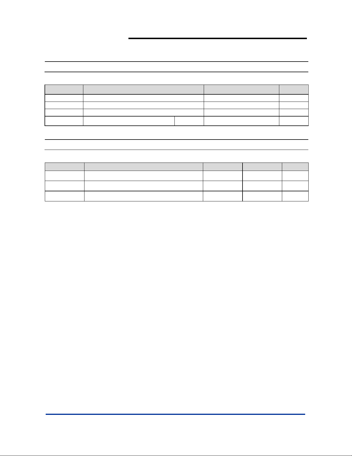
Typical Application Circuit
3.095
AP131 V
3.09
3.085
3.08
3.075
3.07
3.065
out
3.06
V
3.055
3.05
3.045
3.04
3.035
3.03
3.025
3.02
0 30 60 90 120 150 180 210 240 270 300 330
vs. Load Current
out
Load Current (uA
450
400
350
300
250
200
Dropout (V)
150
100
50
0
AP131 Dropout vs. Load
V
=3.3V
OUT
0 50 100 150 200 250 300
Load (Io) (mA)
ON
AP131
V
IN
C
IN
GND
1uF
IN
EN
OUT
BP
C
BP
0.1uF
EN
OFF
V
OUT
C
OUT
10uF
AP131 Rev. 7 5 of 7 FEBRUARY 2009
www.diodes.com © Diodes Incorporated
Page 6

Marking Information
(1) SOT25
AP131
300mA LOW DROPOUT LINEAR REGULATOR WITH
SHUTDOWN
( Top View )
5
7
4
XX : Identification code
Y
: Year 0~9
XX
W X
Y
: Week : A~Z : 1~26 week;
W
a~z : 27~52 week; z represents
52 and 53 week
: a~z : Lead Free
1 2 3
X
A~Z : Green
Part Number Package Identification Code
AP131-15W SOT25 DA
AP131-18W SOT25 DD
AP131-20W SOT25 DF
AP131-25W SOT25 DK
AP131-28W SOT25 DN
AP131-29W SOT25 DO
AP131-30W SOT25 DP
AP131-33W SOT25 DS
AP131-35W SOT25 DU
Package Information (All Dimensions in mm)
AP131 Rev. 7 6 of 7 FEBRUARY 2009
www.diodes.com © Diodes Incorporated
Page 7

AP131
300mA LOW DROPOUT LINEAR REGULATOR WITH
SHUTDOWN
IMPORTANT NOTICE
Diodes Incorporated and its subsidiaries reserve the right to make modifications, enhancements, improvements, corrections or other changes without further
notice to any product herein. Diodes Incorporated does not assume any liability arising out of the application or use of any product described herein; neither
does it convey any license under its patent rights, nor the rights of others. The user of products in such applications shall assume all risks of such use and will
agree to hold Diodes Incorporated and all the companies whose products are represented on our website, harmless against all damages.
LIFE SUPPORT
Diodes Incorporated products are not authorized for use as critical components in life support devices or systems without the expressed written approval of the
President of Diodes Incorporated.
AP131 Rev. 7 7 of 7 FEBRUARY 2009
www.diodes.com © Diodes Incorporated
Page 8

 Loading...