

Page 1
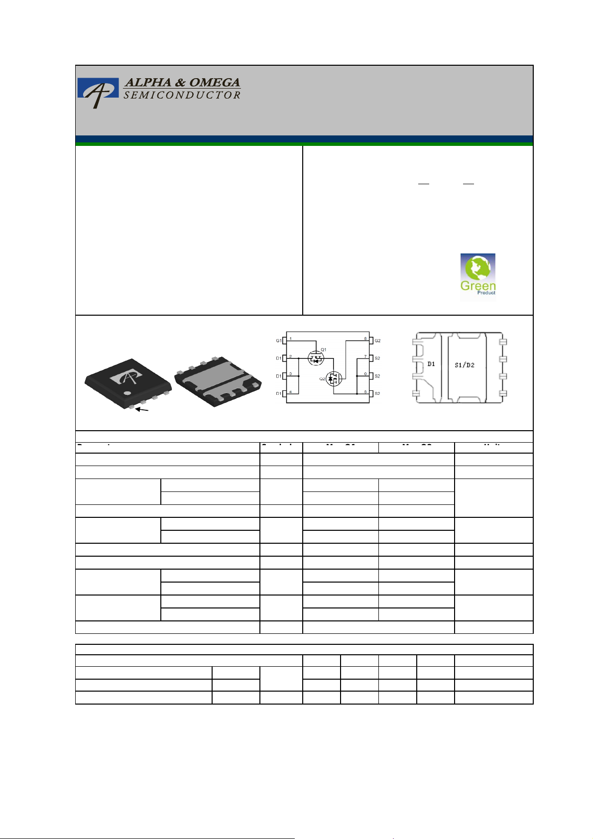
AON6912A
30V Dual Asymmetric N-Channel MOSFET
Q1
Q2
Absolute Maximum Ratings T
=25°C unless otherwise noted
Symbol
A D
C
C
C
Parameter
Units
Max Q1
Max Q2
General Description Product Summary
The AON6912A is designed to provide a high efficiency
synchronous buck power stage with optimal layout and
board space utilization. It includes two specialized
MOSFETs in a dual Power DFN5x6 package. The Q1
"High Side" MOSFET is designed to minimize switching
losses. The Q2 "Low Side" MOSFET is designed for low
R
to reduce conduction losses. The AON6912A is
DS(ON)
well suited for use in compact DC/DC converter
applications.
DFN5X6
DFN5X6
Top View Bottom View
Top View Bottom View
V
DS
ID (at VGS=10V) 34A 52A
R
R
(at VGS=10V) <13.7mΩ <7.3mΩ
DS(ON)
(at VGS = 4.5V) <19.3mΩ <10.4mΩ
DS(ON)
100% UIS Tested
100% Rg Tested
30V 30V
PIN1
PIN1
A
Drain-Source Voltage 30
Gate-Source Voltage
Continuous Drain
Current
TC=25°C
TC=100°C
Pulsed Drain Current
Continuous Drain
Current
TA=25°C
TA=70°C
Avalanche Current
Avalanche Energy L=0.1mH
TC=25°C
B
Power Dissipation
TC=100°C
TA=25°C
A
Power Dissipation
TA=70°C
Junction and Storage Temperature Range °C
V
DS
V
GS
I
D
I
DM
I
DSM
IAS, I
EAS, E
P
D
P
DSM
TJ, T
AR
STG
Top View
Top View
±20
34
21
85
10
8 10.8
22
AR
24 80
22
9
1.9 2.1
1.2 1.3
-55 to 150
52
33
130
13.8
28
30
12
Bottom View
Bottom View
mJ
Thermal Characteristics
Parameter Symbol Typ Q1 Typ Q2 Max Q1 Max Q2
A
Maximum Junction-to-Ambient
Maximum Junction-to-Ambient
Maximum Junction-to-Case
t ≤ 10s
Steady-State
Steady-State
R
θJA
R
θJC
29 24 35 29
56 50 67 60
4.5 3.5 5.5 4.2
Units
°C/W
°C/W
°C/W
V
V
A
A
A
W
W
www.aosmd.com Page 1 of 10
Page 2

tr9
ns
Turn-On Rise Time
Q1 Electrical Characteristics (TJ=25°C unless otherwise noted)
AON6912A
Symbol Min Typ Max Units
Parameter Conditions
STATIC PARAMETERS
BV
I
DSS
I
GSS
V
GS(th)
I
D(ON)
R
DS(ON)
g
FS
V
SD
I
S
Drain-Source Breakdown Voltage
DSS
Zero Gate Voltage Drain Current
Gate-Body leakage current
Gate Threshold Voltage
On state drain current
Static Drain-Source On-Resistance
Forward Transconductance
Diode Forward Voltage
Maximum Body-Diode Continuous Current
ID=250µA, VGS=0V
30 V
VDS=30V, VGS=0V 1
TJ=55°C 5
VDS=0V, VGS= ±20V
VDS=V
GS ID
=250µA
VGS=10V, VDS=5V
VGS=10V, ID=10A
1.5 1.9 2.5 V
85 A
9.8 13.7
100 nA
TJ=125°C 14.5 21.5
VGS=4.5V, ID=10A
VDS=5V, ID=10A
IS=1A,VGS=0V
12.9 19.3 mΩ
45 S
0.75 1 V
µA
mΩ
25 A
DYNAMIC PARAMETERS
C
iss
C
oss
C
rss
R
g
Input Capacitance
Output Capacitance
Reverse Transfer Capacitance
Gate resistance
VGS=0V, VDS=15V, f=1MHz
VGS=0V, VDS=0V, f=1MHz
610 760 910 pF
88 125 160 pF
40 70 100 pF
0.8 1.6 2.4 Ω
SWITCHING PARAMETERS
Qg(10V) 11 14 17.0 nC
Qg(4.5V) 5 6.6 8.0 nC
Q
gs
Q
gd
t
D(on)
Total Gate Charge
Total Gate Charge
Gate Source Charge
Gate Drain Charge
Turn-On DelayTime
VGS=10V, VDS=15V, ID=10A
2.4 nC
3 nC
4.4 ns
VGS=10V, VDS=15V, RL=1.5Ω,
R
t
D(off)
t
f
t
rr
Q
rr
A. The value of R
Power dissipation P
on the user's specific board design.
B. The power dissipation PDis based on T
dissipation limit for cases where additional heatsinking is used.
C. Repetitive rating, pulse width limited by junction temperature T
initial TJ=25°C.
D. The R
E. The static characteristics in Figures 1 to 6 are obtained using <300µs pulses, duty cycle 0.5% max.
F. These curves are based on the junction-to-case thermal impedence which is measured with the device mounted to a large heatsink, assuming
a maximum junction temperature of T
G. The maximum current rating is limited by package.
H. These tests are performed with the device mounted on 1 in2FR-4 board with 2oz. Copper, in a still air environment with TA=25°C.
Turn-Off DelayTime
Turn-Off Fall Time
Body Diode Reverse Recovery Time
Body Diode Reverse Recovery Charge
is measured with the device mounted on 1in2FR-4 board with 2oz. Copper, in a still air environment with TA=25°C. The
θJA
is based on R
DSM
is the sum of the thermal impedence from junction to case R
θJA
and the maximum allowed junction temperature of 150°C. The value in any given application depends
θJA
=150°C, using junction-to-case thermal resistance, and is more useful in setting the upper
J(MAX)
=150°C. The SOA curve provides a single pulse rating.
J(MAX)
GEN
=3Ω
17 ns
6 ns
IF=10A, dI/dt=500A/µs
IF=10A, dI/dt=500A/µs
=150°C. Ratings are based on low frequency and duty cycles to keep
J(MAX)
and case to ambient.
θJC
5.6
6.4
7 8.4 ns
8 9.6
nC
Rev1: Mar. 2011 www.aosmd.com Page 2 of 10
COMPONENTS IN LIFE SUPPORT DEVICES OR SYSTEMS ARE NOT AUTHORIZED. AOS DOES NOT ASSUME ANY LIABILITY ARISING
OUT OF SUCH APPLICATIONS OR USES OF ITS PRODUCTS. AOS RESERVES THE RIGHT TO IMPROVE PRODUCT DESIGN,
FUNCTIONS AND RELIABILITY WITHOUT NOTICE.
Page 3
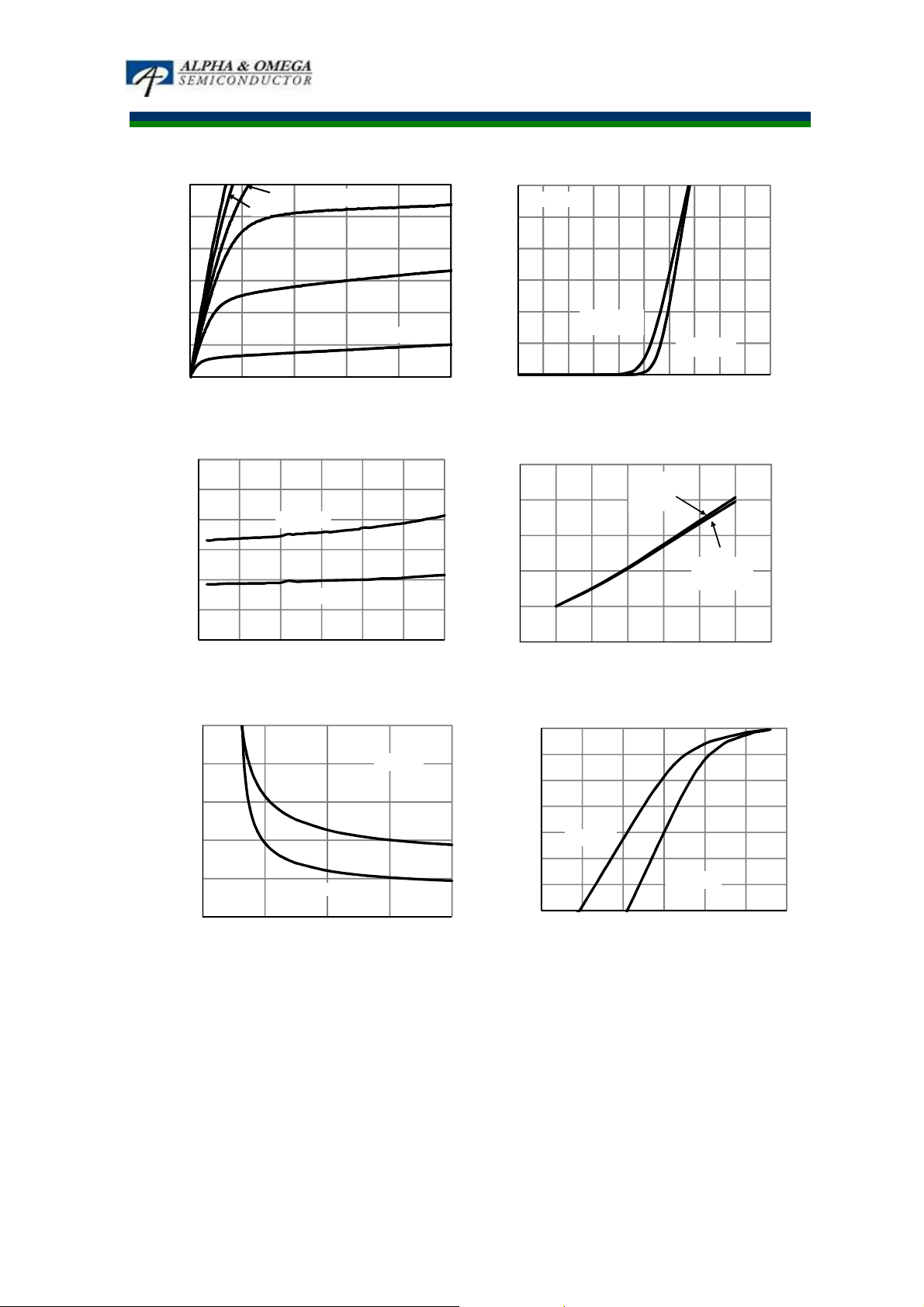
Q1-CHANNEL: TYPICAL ELECTRICAL AND THERMAL CHARACTERISTICS
4.5V
6V
25°C
4.5V
6V
AON6912A
60
60
10V
10V
50
50
4V
4V
30
30
VDS=5V
VDS=5V
25
25
40
40
(A)
(A)
30
30
D
D
I
I
20
20
10
10
0
0
0 1 2 3 4 5
0 1 2 3 4 5
VDS(Volts)
Fig 1: On-Region Characteristics (Note E)
Fig 1: On-Region Characteristics (Note E)
18
18
16
16
14
14
Ω
Ω)
Ω
Ω)
Ω
Ω
Ω
Ω
(m
(m
12
12
DS(ON)
DS(ON)
R
R
10
10
8
8
6
6
0 5 10 15 20 25 30
0 5 10 15 20 25 30
Figure 3: On-Resistance vs. Drain Current and Gate
Figure 3: On-Resistance vs. Drain Current and Gate
30
25
20
Ω
Ω)
Ω
Ω
(m
15
DS(ON)
R
10
5
2 4 6 8 10
Figure 5: On-Resistance vs. Gate-Source Voltage
VDS(Volts)
VGS=4.5V
VGS=4.5V
VGS=10V
VGS=10V
Voltage (Note E)
Voltage (Note E)
VGS(Volts)
(Note E)
ID(A)
ID(A)
3.5V
3.5V
VGS=3V
VGS=3V
ID=10A
125°C
20
20
15
15
(A)
(A)
D
D
I
I
10
10
5
5
0
0
0 0.5 1 1.5 2 2.5 3 3.5 4 4.5 5
0 0.5 1 1.5 2 2.5 3 3.5 4 4.5 5
Figure 2: Transfer Characteristics (Note E)
Figure 2: Transfer Characteristics (Note E)
1.8
1.8
1.6
1.6
1.4
1.4
1.2
1.2
1
1
Normalized On-Resistance
Normalized On-Resistance
0.8
0.8
0 25 50 75 100 125 150 175
0 25 50 75 100 125 150 175
Figure 4: On-Resistance vs. Junction Temperature
Figure 4: On-Resistance vs. Junction Temperature
1.0E+02
1.0E+01
1.0E+00
40
1.0E-01
(A)
S
I
1.0E-02
1.0E-03
1.0E-04
1.0E-05
0.0 0.2 0.4 0.6 0.8 1.0 1.2
Figure 6: Body-Diode Characteristics (Note E)
125°C
125°C
125°C
VGS(Volts)
VGS(Volts)
VGS=10V
VGS=10V
ID=10A
ID=10A
Temperature (°C)
Temperature (°C)
(Note E)
(Note E)
25°C
VSD(Volts)
25°C
25°C
VGS=4.5V
VGS=4.5V
ID=10A
ID=10A
17
5
2
10
0
18
Rev1: Mar. 2011 www.aosmd.com Page 3 of 10
Page 4

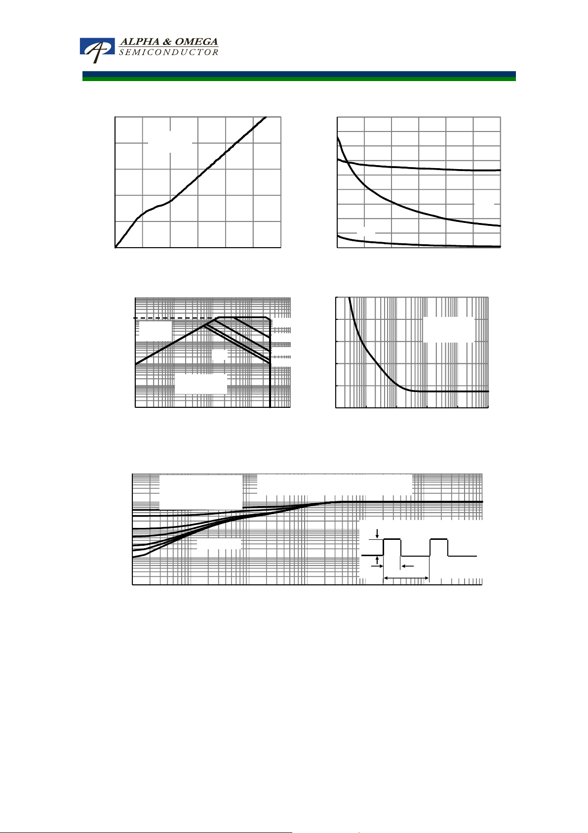
Q1-CHANNEL: TYPICAL ELECTRICAL AND THERMAL CHARACTERISTICS
10µs
Case (Note F)
10µs
on
P
10
10
VDS=15V
VDS=15V
ID=10A
ID=10A
8
8
6
6
(Volts)
(Volts)
GS
GS
4
4
V
V
2
2
0
0
0 2 4 6 8 10
0 2 4 6 8 10
Figure 7: Gate-Charge Characteristics
Figure 7: Gate-Charge Characteristics
1000.0
1000.0
100.0
100.0
R
R
DS(ON)
DS(ON)
limited
limited
10.0
10.0
(Amps)
(Amps)
1.0
1.0
D
D
I
I
0.1
0.1
Qg(nC)
Qg(nC)
T
=150°C
T
=150°C
J(Max)
J(Max)
TC=25°C
TC=25°C
DC
DC
100us
100us
1ms
1ms
1200
1200
1000
1000
C
C
iss
800
800
600
600
400
400
Capacitance (pF)
Capacitance (pF)
200
200
C
C
rss
rss
0
0
0 5 10 15 20 25 30
0 5 10 15 20 25 30
Figure 8: Capacitance Characteristics
Figure 8: Capacitance Characteristics
200
200
160
160
120
120
80
80
Power (W)
Power (W)
40
40
iss
C
C
oss
oss
VDS(Volts)
VDS(Volts)
T
T
J(Max)
J(Max)
TC=25°C
TC=25°C
=150°C
=150°C
AON6912A
0.0
0.0
0.01 0.1 1 10 100
0.01 0.1 1 10 100
Figure 9: Maximum Forward Biased
Figure 9: Maximum Forward Biased
VDS(Volts)
VDS(Volts)
Safe Operating Area (Note F)
10
1
D=Ton/T
T
J,PK=TC+PDM.ZθJC.RθJC
R
=5.5°C/W
θJC
In descending order
D=0.5, 0.3, 0.1, 0.05, 0.02, 0.01, single pulse
0
0
0.0001 0.001 0.01 0.1 1 10
0.0001 0.001 0.01 0.1 1 10
Pulse Width (s)
Figure 10: Single Pulse Power Rating Junction-to-
Figure 10: Single Pulse Power Rating Junction-to-
Pulse Width (s)
Case (Note F)
0.1
Normalized Transient
Thermal Resistance
0.01
θ
θJC
θ
θ
Z
Single Pulse
T
T
0.001
0.00001 0.0001 0.001 0.01 0.1 1 10
Figure 11: Normalized Maximum Transient Thermal Impedance (Note F)
Pulse Width (s)
Rev1: Mar. 2011 www.aosmd.com Page 4 of 10
Page 5

Q1-CHANNEL: TYPICAL ELECTRICAL AND THERMAL CHARACTERISTICS
100
100
TA=25°C
TA=25°C
TA=100°C
TA=100°C
TA=150°C
TA=150°C
TA=125°C
TA=125°C
(A) Peak Avalanche Current
(A) Peak Avalanche Current
AR
AR
I
I
10
10
0.000001 0.00001 0.0001 0.001
0.000001 0.00001 0.0001 0.001
Time in avalanche, tA(s)
Figure 12: Single Pulse Avalanche capability (Note
Figure 12: Single Pulse Avalanche capability (Note
40
40
35
35
30
30
(A)
(A)
D
D
25
25
20
20
15
15
Current rating I
Current rating I
10
10
5
5
0
0
0 25 50 75 100 125 150
0 25 50 75 100 125 150
Time in avalanche, tA(s)
C)
C)
T
(°°°°C)
T
(°°°°C)
CASE
Figure 14: Current De-rating (Note F)
Figure 14: Current De-rating (Note F)
CASE
25
25
20
20
15
15
10
10
Power Dissipation (W)
Power Dissipation (W)
5
5
0
0
0 25 50 75 100 125 150
0 25 50 75 100 125 150
T
(°°°°C)
T
(°°°°C)
CASE
CASE
TA=25°C
TA=25°C
10000
10000
1000
1000
Figure 13: Power De-rating (Note F)
Figure 13: Power De-rating (Note F)
17
100
100
Power (W)
Power (W)
10
10
1
1
0.00001 0.001 0.1 10 1000
0.00001 0.001 0.1 10 1000
Figure 15: Single Pulse Power Rating Junction-to-
Figure 15: Single Pulse Power Rating Junction-to-
Pulse Width (s)
Pulse Width (s)
Ambient (Note H)
10
18
AON6912A
5
2
0
10
1
D=Ton/T
T
J,PK=TA+PDM.ZθJA.RθJA
R
=67°C/W
θJA
In descending order
D=0.5, 0.3, 0.1, 0.05, 0.02, 0.01, single pulse
40
0.1
Normalized Transient
Thermal Resistance
0.01
θ
θJA
θ
θ
Z
Single Pulse
0.001
0.00001 0.0001 0.001 0.01 0.1 1 10 100 1000
Figure 16: Normalized Maximum Transient Thermal Impedance (Note H)
Pulse Width (s)
Rev1: Mar. 2011 www.aosmd.com Page 5 of 10
Page 6

tr2
ns
Turn-On Rise Time
Q2 Electrical Characteristics (TJ=25°C unless otherwise noted)
AON6912A
Symbol Min Typ Max Units
Parameter Conditions
STATIC PARAMETERS
BV
I
DSS
I
GSS
V
GS(th)
I
D(ON)
R
DS(ON)
g
FS
V
SD
I
S
Drain-Source Breakdown Voltage
DSS
Zero Gate Voltage Drain Current
Gate-Body leakage current
Gate Threshold Voltage
On state drain current
Static Drain-Source On-Resistance
Forward Transconductance
Diode Forward Voltage
Maximum Body-Diode Continuous Current
ID=250µA, VGS=0V
30 V
VDS=30V, VGS=0V 1
TJ=55°C 5
VDS=0V, VGS= ±20V
VDS=V
GS ID
=250µA
VGS=10V, VDS=5V
VGS=10V, ID=20A
1.3 1.9 2.5 V
130 A
6.1 7.3
100 nA
TJ=125°C 8.5 10.2
VGS=4.5V, ID=20A
VDS=5V, ID=20A
IS=1A,VGS=0V
8.3 10.4 mΩ
60 S
0.7 1 V
µA
mΩ
35 A
DYNAMIC PARAMETERS
C
iss
C
oss
C
rss
R
g
Input Capacitance
Output Capacitance
Reverse Transfer Capacitance
Gate resistance
VGS=0V, VDS=15V, f=1MHz
VGS=0V, VDS=0V, f=1MHz
870 1090 1300 pF
340 490 640 pF
22 38 53 pF
0.4 0.9 1.4 Ω
SWITCHING PARAMETERS
Qg(10V) 12 16 20 nC
Qg(4.5V) 5 7 9 nC
Q
gs
Q
gd
t
D(on)
Total Gate Charge
Total Gate Charge
Gate Source Charge
Gate Drain Charge
Turn-On DelayTime
VGS=10V, VDS=15V, ID=20A
2 2.5 3 nC
1.5 2.5 3.5 nC
5 ns
VGS=10V, VDS=15V, RL=0.75Ω,
R
t
D(off)
t
f
t
rr
Q
rr
A. The value of R
Power dissipation P
on the user's specific board design.
B. The power dissipation PDis based on T
dissipation limit for cases where additional heatsinking is used.
C. Repetitive rating, pulse width limited by junction temperature T
initial TJ =25°C.
D. The R
E. The static characteristics in Figures 1 to 6 are obtained using <300µs pulses, duty cycle 0.5% max.
F. These curves are based on the junction-to-case thermal impedence which is measured with the device mounted to a large heatsink, assuming
a maximum junction temperature of T
G. These tests are performed with the device mounted on 1 in2FR-4 board with 2oz. Copper, in a still air environment with TA=25°C.
Turn-Off DelayTime
Turn-Off Fall Time
Body Diode Reverse Recovery Time
Body Diode Reverse Recovery Charge
is measured with the device mounted on 1in2FR-4 board with 2oz. Copper, in a still air environment with TA=25°C. The
θJA
is based on R
DSM
is the sum of the thermal impedence from junction to case R
θJA
and the maximum allowed junction temperature of 150°C. The value in any given application depends
θJA
=150°C, using junction-to-case thermal resistance, and is more useful in setting the upper
J(MAX)
=150°C. The SOA curve provides a single pulse rating.
J(MAX)
GEN
=3Ω
16 ns
2 ns
IF=20A, dI/dt=500A/µs
IF=20A, dI/dt=500A/µs
=150°C. Ratings are based on low frequency and duty cycles to keep
J(MAX)
and case to ambient.
θJC
10
20
13 16 ns
25 30
nC
Rev1: Mar. 2011 www.aosmd.com Page 6 of 10
COMPONENTS IN LIFE SUPPORT DEVICES OR SYSTEMS ARE NOT AUTHORIZED. AOS DOES NOT ASSUME ANY LIABILITY ARISING
OUT OF SUCH APPLICATIONS OR USES OF ITS PRODUCTS. AOS RESERVES THE RIGHT TO IMPROVE PRODUCT DESIGN,
FUNCTIONS AND RELIABILITY WITHOUT NOTICE.
Page 7

Q2-CHANNEL: TYPICAL ELECTRICAL AND THERMAL CHARACTERISTICS
25°C
100
100
10V
10V
4.5V
4.5V
80
80
60
60
(A)
(A)
D
D
I
I
40
40
20
20
0
0
0 1 2 3 4 5
0 1 2 3 4 5
VDS(Volts)
Fig 1: On-Region Characteristics (Note E)
Fig 1: On-Region Characteristics (Note E)
15
15
12
12
Ω
Ω)
Ω
Ω)
Ω
Ω
Ω
Ω
9
9
(m
(m
6
6
DS(ON)
DS(ON)
R
R
3
3
0
0
0 5 10 15 20 25 30
0 5 10 15 20 25 30
Figure 3: On-Resistance vs. Drain Current and Gate
Figure 3: On-Resistance vs. Drain Current and Gate
VDS(Volts)
Voltage (Note E)
Voltage (Note E)
VGS=4.5V
VGS=4.5V
ID(A)
ID(A)
4V
4V
VGS=10V
VGS=10V
3.5V
3.5V
VGS=3V
VGS=3V
50
50
VDS=5V
VDS=5V
40
40
30
30
(A)
(A)
D
D
I
I
20
20
10
10
0
0
1 1.5 2 2.5 3 3.5 4
1 1.5 2 2.5 3 3.5 4
Figure 2: Transfer Characteristics (Note E)
Figure 2: Transfer Characteristics (Note E)
1.6
1.6
1.4
1.4
1.2
1.2
1
1
Normalized On-Resistance
Normalized On-Resistance
0.8
0.8
0 25 50 75 100 125 150 175
0 25 50 75 100 125 150 175
125°C
125°C
25°C
25°C
VGS(Volts)
VGS(Volts)
VGS=10V
VGS=10V
ID=20A
ID=20A
VGS=4.5V
VGS=4.5V
ID=20A
ID=20A
Temperature (°C)
Figure 4: On-Resistance vs. Junction Temperature
Figure 4: On-Resistance vs. Junction Temperature
Temperature (°C)
(Note E)
(Note E)
AON6912A
17
5
2
10
0
18
30
25
20
Ω
Ω)
Ω
Ω
(m
15
DS(ON)
R
10
5
0
2 4 6 8 10
Figure 5: On-Resistance vs. Gate-Source Voltage
125°C
VGS(Volts)
(Note E)
ID=20A
1.0E+02
1.0E+01
1.0E+00
1.0E-01
(A)
S
I
1.0E-02
1.0E-03
1.0E-04
1.0E-05
40
125°C
25°C
0.0 0.2 0.4 0.6 0.8 1.0 1.2
Figure 6: Body-Diode Characteristics (Note E)
VSD(Volts)
Rev1: Mar. 2011 www.aosmd.com Page 7 of 10
Page 8
Q2-CHANNEL: TYPICAL ELECTRICAL AND THERMAL CHARACTERISTICS
10µs
1ms
100µs
C
10ms
10µs
1ms
100µs
C
on
P
10ms
AON6912A
10
10
VDS=15V
8
8
6
6
(Volts)
(Volts)
GS
GS
4
4
V
V
2
2
0
0
0 3 6 9 12 15 18
0 3 6 9 12 15 18
1000.0
1000.0
100.0
100.0
10.0
10.0
(Amps)
(Amps)
1.0
1.0
D
D
I
I
0.1
0.1
VDS=15V
ID=20A
ID=20A
Qg(nC)
Figure 7: Gate-Charge Characteristics
Figure 7: Gate-Charge Characteristics
R
R
DS(ON)
DS(ON)
limited
limited
Qg(nC)
T
T
J(Max)
J(Max)
DC
DC
=150°C
=150°C
1800
1800
1600
1600
1400
1400
1200
1200
1000
1000
800
800
600
600
Capacitance (pF)
Capacitance (pF)
400
400
200
200
0
0
0 5 10 15 20 25 30
0 5 10 15 20 25 30
Figure 8: Capacitance Characteristics
Figure 8: Capacitance Characteristics
200
200
160
160
120
120
80
80
Power (W)
Power (W)
40
40
VDS(Volts)
VDS(Volts)
C
C
iss
iss
T
=150°C
T
=150°C
J(Max)
J(Max)
TC=25°C
TC=25°C
C
C
oss
oss
0.0
0.0
0.01 0.1 1 10 100
0.01 0.1 1 10 100
Figure 9: Maximum Forward Biased Safe
Figure 9: Maximum Forward Biased Safe
10
D=Ton/T
T
1
R
VDS(Volts)
VDS(Volts)
Operating Area (Note F)
Operating Area (Note F)
J,PK=TC+PDM.ZθJC.RθJC
=4.2°C/W
θJC
In descending order
D=0.5, 0.3, 0.1, 0.05, 0.02, 0.01, single pulse
0
0
0.0001 0.001 0.01 0.1 1 10
0.0001 0.001 0.01 0.1 1 10
Pulse Width (s)
Figure 10: Single Pulse Power Rating Junction-to-
Figure 10: Single Pulse Power Rating Junction-to-
Pulse Width (s)
Case (Note F)
Case (Note F)
40
0.1
Normalized Transient
Thermal Resistance
0.01
θ
θJC
θ
θ
Z
Single Pulse
T
T
0.001
0.00001 0.0001 0.001 0.01 0.1 1 10
Figure 11: Normalized Maximum Transient Thermal Impedance (Note F)
Pulse Width (s)
Rev1: Mar. 2011 www.aosmd.com Page 8 of 10
Page 9

Q2-CHANNEL: TYPICAL ELECTRICAL AND THERMAL CHARACTERISTICS
on
P
100
100
TA=25°C
TA=25°C
TA=100°C
TA=100°C
TA=125°C
TA=125°C
TA=150°C
TA=150°C
(A) Peak Avalanche Current
(A) Peak Avalanche Current
AR
AR
I
I
10
10
0.000001 0.00001 0.0001 0.001
0.000001 0.00001 0.0001 0.001
Figure 12: Single Pulse Avalanche capability (Note
Figure 12: Single Pulse Avalanche capability (Note
60
60
50
50
(A)
(A)
D
D
40
40
30
30
20
20
Current rating I
Current rating I
10
10
Time in avalanche, tA(s)
Time in avalanche, tA(s)
C)
C)
AON6912A
35
35
30
30
25
25
20
20
15
15
10
10
Power Dissipation (W)
Power Dissipation (W)
5
5
0
0
0 25 50 75 100 125 150
0 25 50 75 100 125 150
Figure 13: Power De-rating (Note F)
Figure 13: Power De-rating (Note F)
10000
10000
1000
1000
100
100
Power (W)
Power (W)
10
10
T
T
CASE
CASE
(°°°°C)
(°°°°C)
TA=25°C
TA=25°C
17
10
5
2
1
0
0
0 25 50 75 100 125 150
0 25 50 75 100 125 150
Figure 14: Current De-rating (Note F)
Figure 14: Current De-rating (Note F)
10
1
T
(°°°°C)
T
(°°°°C)
CASE
CASE
D=Ton/T
T
J,PK=TA+PDM.ZθJA.RθJA
R
=60°C/W
θJA
In descending order
D=0.5, 0.3, 0.1, 0.05, 0.02, 0.01, single pulse
1
0.00001 0.001 0.1 10 1000
0.00001 0.001 0.1 10 1000
Figure 15: Single Pulse Power Rating Junction-to-
Figure 15: Single Pulse Power Rating Junction-to-
Pulse Width (s)
Pulse Width (s)
Ambient (Note G)
40
0.1
Normalized Transient
Thermal Resistance
0.01
θ
θJA
θ
θ
Z
Single Pulse
0.001
T
T
0.0001 0.001 0.01 0.1 1 10 100 1000
Figure 16: Normalized Maximum Transient Thermal Impedance (Note G)
Pulse Width (s)
0
18
Rev1: Mar. 2011 www.aosmd.com Page 9 of 10
Page 10

VDC
VDC
Rg
Rg
AON6912A
Gate Charge Test Circuit & Waveform
Gate Charge Test Circuit & Waveform
Vgs
Vgs
Qg
Qg
10V
Vds
Vds
10V
Qgs
Qgs
Qgd
Qgd
Charge
Charge
90%
90%
10%
10%
+
+
-
-
Vgs
Vgs
Ig
Ig
RL
RL
Vds
Vds
DUT
Vgs
Vgs
DUT
+
+
Vds
Vds
VDC
VDC
-
-
DUT
DUT
Resistive Switching Test Circuit & Waveforms
Resistive Switching Test Circuit & Waveforms
+
+
Vdd
Vdd
VDC
VDC
-
-
Vgs
Vds +
Vds -
Ig
Vgs
Vgs
Rg
Vgs
Isd
Vgs
Vds
Vds
Id
Id
DUT
Vgs
Vgs
Unclamped Inductive Switching (UIS) Test Circuit & Waveforms
Unclamped Inductive Switching (UIS) Test Circuit & Waveforms
L
L
Vgs
+
Vdd
VDC
-
Vds
Vds
Id
t t
t t
r
r
d(on)
d(on)
t
t
on
on
E = 1/2 LI
E = 1/2 LI
AR
AR
t
t
t
t
d(off)
d(off)
t
t
off
off
2
2
AR
AR
DUT
Vgs
Diode Recovery Test Circuit & Waveforms
Q = - Idt
rr
Vgs
t
L
+
Vdd
VDC
-
Isd
Vds
I
F
dI/dt
rr
I
RM
f
f
BV
BV
DSS
DSS
I
AR
Vdd
Rev1: Mar. 2011 www.aosmd.com Page 10 of 10
Page 11

Page 12

 Loading...