

Page 1
p
AO3407
A
P-Channel Enhancement Mode Field Effect Transistor
ug 2002
General Description
The AO3407 uses advanced trench technology to
provide excellent R
device is suitable for use as a load switch or in PWM
applications.
Absolute Maximum Ratings T
Drain-Source Voltage -30
Continuous Drain
Current
A
Pulsed Drain Current
Power Dissipation
A
Junction and Storage Temperature Range
with low gate charge. This
DS(ON)
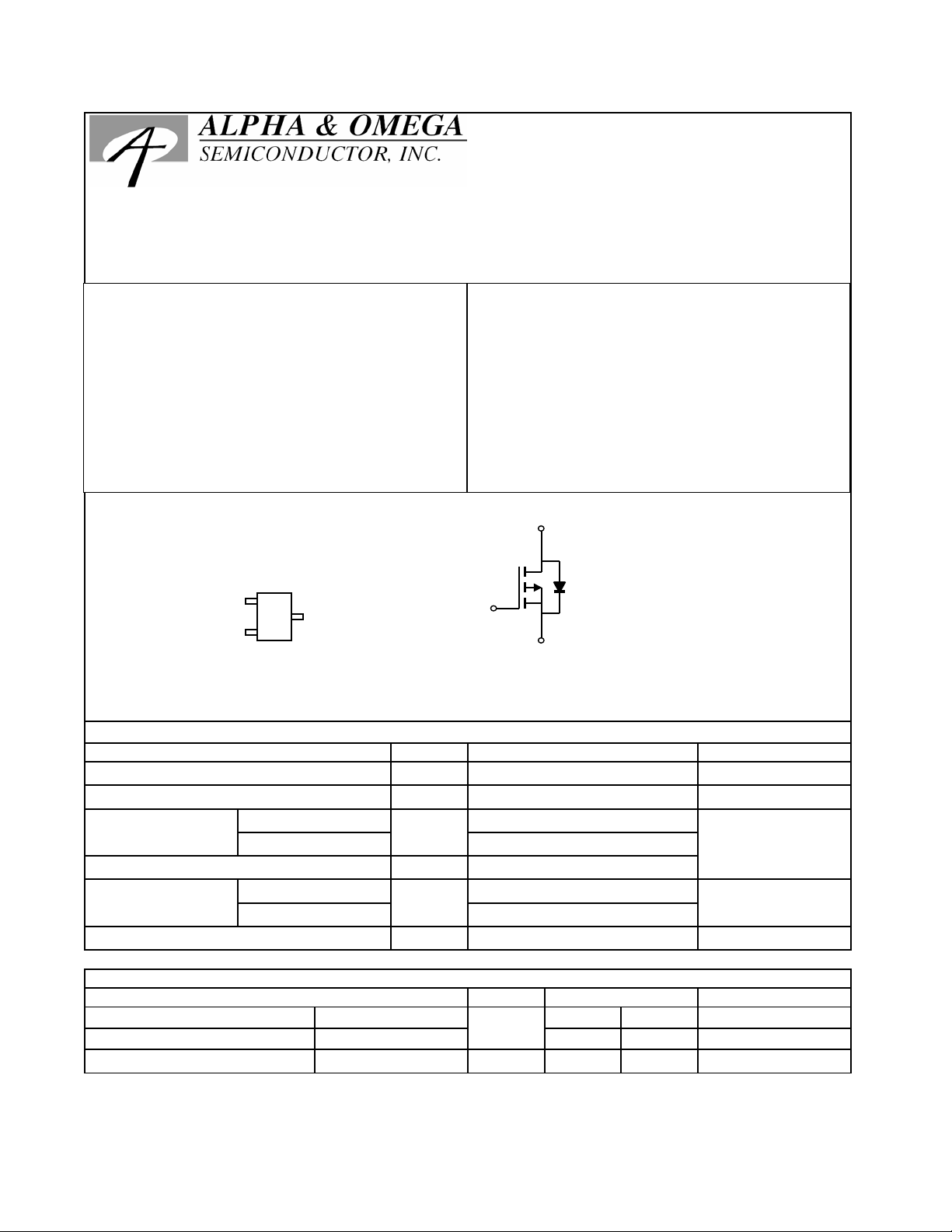
TO-236
(SOT-23)
Top View
G
D
S
=25°C unless otherwise noted
A
=25°C
T
A
=70°C
T
A
B
TA=25°C
=70°C
T
A
Symbol
V
DS
V
GS
I
D
I
DM
P
D
TJ, T
STG
Features
VDS (V) = -30V
I
= -4.1 A
D
R
R
G
< 52mΩ (VGS = -10V)
DS(ON)
< 87mΩ (VGS = -4.5V)
DS(ON)
D
S
Maximum UnitsParameter
±20Gate-Source Voltage
-4.1
-3.5
-20
1.4
-55 to 150
1
V
V
A
W
°C
Thermal Characteristics
Parameter Units
Maximum Junction-to-Ambient
Maximum Junction-to-Ambient
Maximum Junction-to-Lead
C
A
A
t ≤ 10s
Steady-State
Steady-State
Symbol Ty
R
θJA
R
θJL
65 90
85 125
43 60
Max
°C/W
°C/W
°C/W
Alpha & Omega Semiconductor, Ltd.
Page 2
AO3407
Ω
Electrical Characteristics (TJ=25°C unless otherwise noted)
Symbol Min Typ Max Units
Parameter Conditions
STATIC PARAMETERS
BV
I
DSS
I
GSS
V
GS(th)
I
D(ON)
R
DS(ON)
g
FS
V
SD
I
S
DSS
Drain-Source Breakdown Voltage
Zero Gate Voltage Drain Current
Gate-Body leakage current
ID=-250µA, VGS=0V
VDS=-24V, VGS=0V
VDS=0V, VGS=±20V
Gate Threshold Voltage VDS=V
On state drain current
VGS=-4.5V, VDS=-5V
VGS=-10V, ID=-4.1A
Static Drain-Source On-Resistance
VGS=-4.5V, ID=-3A
Forward Transconductance
Diode Forward Voltage
VDS=-5V, ID=-4A
IS=-1A,VGS=0V
Maximum Body-Diode Continuous Current
GS ID
TJ=55°C
=-250µA
TJ=125°C
-30 V
-1
-5
µA
±100 nA
-1 -1.8 -3 V
-10 A
40.5 52
57 73
64 87
mΩ
m
5.5 8.2 S
-0.77 -1 V
-2.2 A
DYNAMIC PARAMETERS
C
iss
C
oss
C
rss
R
g
Input Capacitance
Output Capacitance
VGS=0V, VDS=-15V, f=1MHz
Reverse Transfer Capacitance
Gate resistance VGS=0V, VDS=0V, f=1MHz
700 pF
120 pF
75 pF
10 Ω
SWITCHING PARAMETERS
Q
Q
Q
Q
t
D(on)
t
r
t
D(off)
t
f
t
rr
Q
g
g
gs
gd
Total Gate Charge (10V)
Total Gate Charge (4.5V)
Gate Source Charge
Gate Drain Charge
VGS=-4.5V, VDS=-15V, ID=-4A
Turn-On DelayTime
Turn-On Rise Time
Turn-Off DelayTime
VGS=-10V, VDS=-15V, RL=3.6Ω,
R
=3Ω
GEN
Turn-Off Fall Time
Body Diode Reverse Recovery Time
rr
Body Diode Reverse Recovery Charge
IF=-4A, dI/dt=100A/µs
IF=-4A, dI/dt=100A/µs
14.3 nC
7nC
3.1 nC
3nC
8.6 ns
5ns
28.2 ns
13.5 ns
27
ns
15 nC
A: The value of R
value in any a given application depends on the user's specific board design. The current rating is based on the t ≤ 10s thermal resistance
rating.
B: Repetitive rating, pulse width limited by junction temperature.
C. The R
θJA
D. The static characteristics in Figures 1 to 6,12,14 are obtained using 80 µs pulses, duty cycle 0.5% max.
E. These tests are performed with the device mounted on 1 in
SOA curve provides a single pulse rating.
is measured with the device mounted on 1in 2 FR-4 board with 2oz. Copper, in a still air environment with T
θJA
is the sum of the thermal impedence from junction to lead R
2
FR-4 board with 2oz. Copper, in a still air environment with T A=25°C. The
and lead to ambient.
θJL
=25°C. The
A
Alpha & Omega Semiconductor, Ltd.
Page 3
AO3407
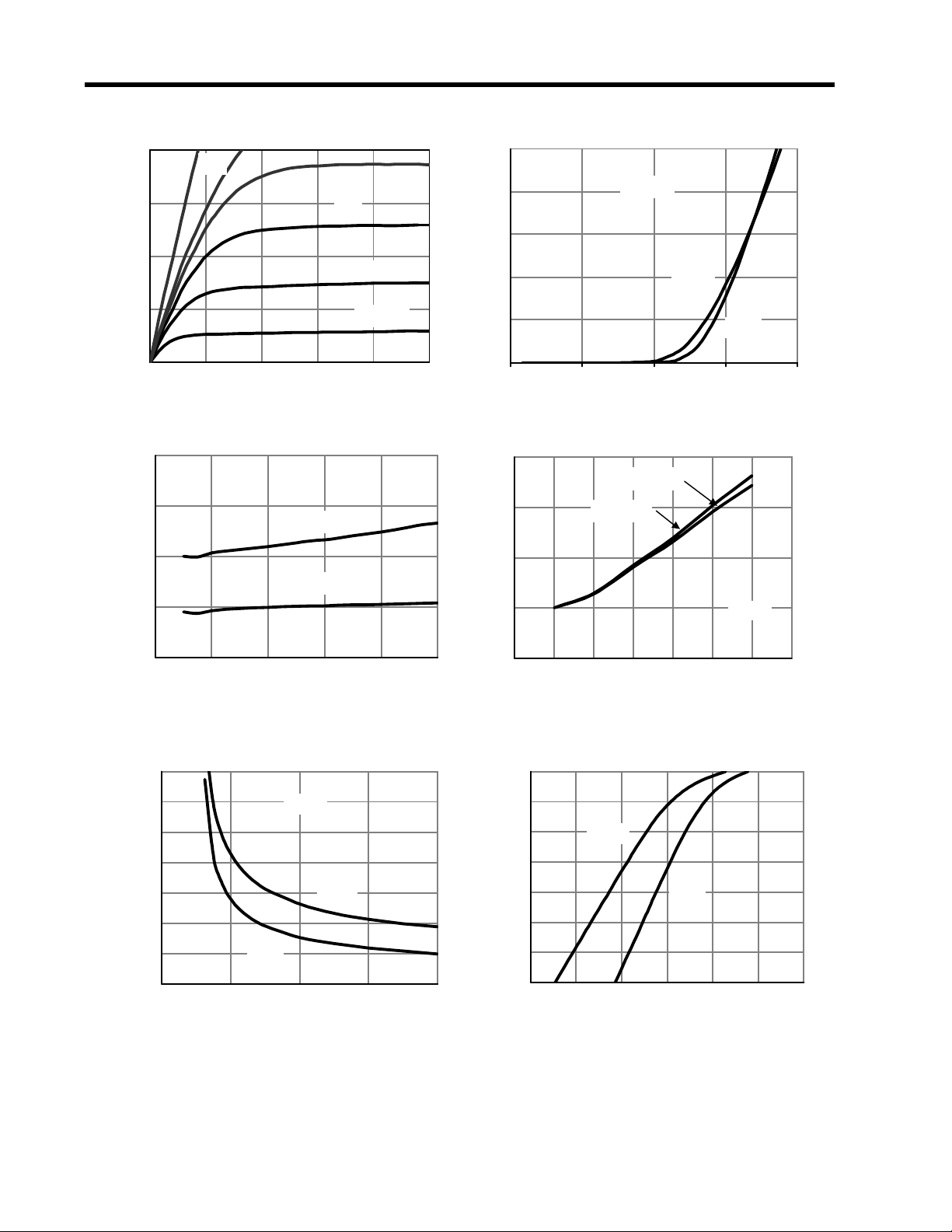
TYPICAL ELECTRICAL AND THERMAL CHARACTERISTICS
20
-10V
-5V
-4.5V
15
10
(A)
D
-I
5
-4V
-3.5V
VGS=-3V
0
0.00 1.00 2.00 3.00 4.00 5.00
(Volts)
-V
DS
Figure 1: On-Region Characteristics
100
80
)
Ω
(m
DS(ON)
R
60
VGS=-4.5V
VGS=-10V
40
10
8
VDS=-5V
6
(A)
D
-I
4
2
125°C
25°C
0
01234
-V
(Volts)
GS
Figure 2: Transfer Characteristics
1.6
VGS=-4.5V
1.4
VGS=-10V
1.2
1
ID=-2A
Normalized On-Resistance
20
0246810
(A)
-I
D
Figure 3: On-Resistance vs. Drain Current and
Gate Voltage
160
140
ID=-2A
120
)
Ω
100
(m
80
DS(ON)
R
60
40
25°C
125°C
20
246810
-V
(Volts)
GS
Figure 5: On-Resistance vs. Gate-Source Voltage
0.8
0 25 50 75 100 125 150 175
Temperature (°C)
Figure 4: On-Resistance vs. Junction
Temperature
1E+01
1E+00
1E-01
1E-02
(A)
S
-I
1E-03
125°C
25°C
1E-04
1E-05
1E-06
0.0 0.2 0.4 0.6 0.8 1.0 1.2
-V
(Volts)
SD
Figure 6: Body-Diode Characteristics
Alpha and Omega Semiconductor, Ltd.
Page 4

AO3407
S
0.1s1s10sDC
TYPICAL ELECTRICAL AND THERMAL CHARACTERISTIC
10
VDS=-15V
=-4A
8
I
D
6
(Volts)
GS
4
-V
2
0
0481216
-Q
(nC)
g
Figure 7: Gate-Charge Characteristics
100
10
T
J(Max)
T
=25°C
A
R
DS(ON)
limited
=150°C
100µs
10µs
1ms
(Amps)
D
-I
1
10ms
1000
800
C
iss
600
400
Capacitance (pF)
C
oss
C
rss
200
0
0 5 10 15 20 25 30
-V
(Volts)
DS
Figure 8: Capacitance Characteristics
40
T
J(Max)
T
A
30
20
Power (W)
10
=150°C
=25°C
0.1
0.1 1 10 100
-V
(Volts)
DS
Figure 9: Maximum Forward Biased Safe
Operating Area (Note E)
10
D=Ton/T
T
J,PK=TA+PDM.ZθJA.RθJA
R
=90°C/W
θJA
In descending order
D=0.5, 0.3, 0.1, 0.05, 0.02, 0.01, single pulse
0
0.001 0.01 0.1 1 10 100 1000
Pulse Width (s)
Figure 10: Single Pulse Power Rating Junction-to-
Ambient (Note E)
1
0.1
Normalized Transient
Thermal Resistance
θJA
Z
P
T
T
Single Pulse
0.01
0.00001 0.0001 0.001 0.01 0.1 1 10 100 1000
Pulse Width (s)
Figure 11: Normalized Maximum Transient Thermal Impedance
Alpha & Omega Semiconductor, Ltd.
Page 5

SOT-23 Package Data
θ
GAUGE PLANE
SEATING PLANE
SYMBOLS
A
A1
A2
DIMENSIONS IN MILLIMETERS
MIN
1.00
0.00
1.00
−−−
1.10
MAXNOM
1.25−−−
0.10
1.15
0.500.40b 0.35
C
D
E
E1 1.40
e
0.10
2.80
2.60
−−−
0.15
2.90
2.80
1.60
0.95 BSC
0.25
3.04
2.95
1.80
−−−
e1 −−− 1.90 BSC −−−
L
0.40
−−−
0.60
5° 8°θ1 1°
NOTE:
1. LEAD FINISH: 150 MICROINCHES ( 3.8 um) MIN.
THICKNESS OF Tin/Lead (SOLDER) PLATED ON LEAD
2. TOLERANCE ±0.10 mm (4 mil) UNLESS OTHERWISE
SPECIFIED
3. COPLANARITY : 0.10 mm
4. DIMENSION L IS MEASURED IN GAGE PLANE
PACKAGE MARKING DESCRIPTION
P N D L N
NOTE:
P N - PART NUMBER CODE.
D - YAER AND WEEK CODE.
L N - ASSEMBLY LOT CODE, FAB AND
ASSEMBLY LOCATION CODE.
SOT-23 PART NO. CODE
PART NO.
CODE
AO3407 A7
RECOMMENDATION OF LAND PATTERN
Rev. A
Page 6

ALPHA & OMEGA
SEMICONDUCTOR, INC.
SOT-23 Carrier Tape
SOT-23 Reel
SOT-23 Tape and Reel Data
SOT-23 Tape
Leader / Trailer
& Orientation
Page 7

 Loading...