

Page 1
ICs for TV
■ Overview
The AN96A07K is a dynamic astigmatizm and focus
(DAF)IC for CRT monitor. It outputs parabola waves for
focus control.
■ Features
●
fH=15 to 90kHz, fV = 50 to 120Hz
●
Constant-amplitude parabola-wave output following
input frequency
●
Coefficient of parabola-wave is controlled by an external resistor
AN96A07K
Dynamic Focus Controller IC for CRT Monitor
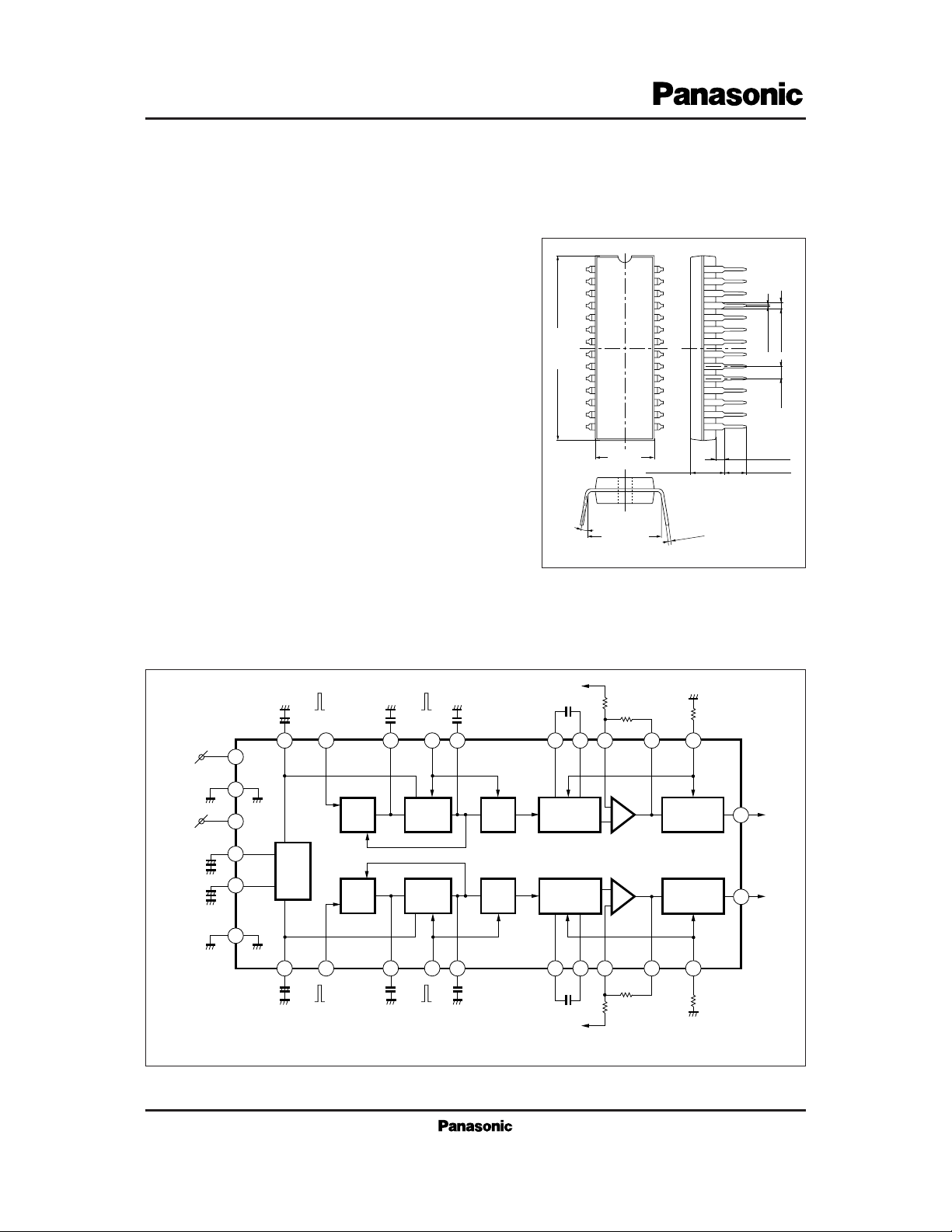
Unit : mm
26.7±0.3
8.4±0.3
10.16±0.25
3 to 15˚
0.45
–
0
.0
5
+
0
.1
0.9±0.25
0.5±0.1
1.778
4.80±0.25 3.05±0.25
1.05±0.25
28-Pin SDIP Package (SDI 028-P-0400)
■ Block Diagram
To Pin28
100pF
1µF
+
V
CC1
18 27 17 26 19
0.1µF
0.27µF
20 21 23 24 22
25
15
V
1µF
1µF
CC2
+
+
5
28
REF
DC
2
HOLD
HOLD
SAW –
TOOTH
SAW –
TOOTH
ABS.
ABS.
LIN – LOG
Conv.
LIN – LOG
Conv.
1
7 3 6 4 8 9 10 12 13 11
+
1µF
0.1µF
330pF
100pF
To Pin28
10kΩ
10kΩ
–
+
+
–
10kΩ
10kΩ
220kΩ
LIN – LOG
Conv.
LIN – LOG
Conv.
220kΩ
16
14
Page 2
ICs for TV
AN96A07K
GND
Reference bias output (6V)
Hor. sampling pulse input
Hor. phase shift pulse input
Pin No.
1
2
3
4
Pin name
GND
Ver. parabola output
Holding
Ver. system reference bias output (2V)
Pin name
Pin No.
V
CC1
(12V)
Holding
Hor. system reference bias output (2V)
5
6
7
Triangular waveform generation capacitor
Oscillation prevention capacitor
Oscillation prevention capacitor
Triangular waveform generation capacitor
8
Ver. parabola output amplitude adj.
Oscillation prevention capacitor
Oscillation prevention capacitor
Hor. parabola output amplitude adj.
9
10
11
Feedback input
Feedback output
V
CC2
(12V)
Feedback input
Feedback output
Hor. parabola output
12
13
14
Ver. phase shift pulse input
Ver. sampling pulse input
Reference bias output (4V)
20
16
17
18
19
25
26
27
28
21
22
23
24
15
■ Pin Descriptions
Supply current
Supply voltage
Power dissipation
Note 2)
Operating ambient temperature
Note 1)
Storage temperature
Note 1)
V
mW
mA
˚C
˚C
Note 1) Ta= 25˚C except operating ambient temperature and storage temperature.
Note 2) Allowable power dissipation of the package at Ta=75˚C.
■ Absolute Maximum Ratings
Parameter Symbol Rating Unit
V
CC
I
CC
P
D
T
opr
T
stg
13.4
30
402
– 20 to + 75
– 55 to + 150
Parameter Symbol Range
Operating supply voltage range
V
CC
9.6V to 13.2V
■ Recommended Operating Range (Ta= 25˚C)
Page 3
ICs for TV
AN96A07K
Parameter minCondition typ max UnitSymbol
I
CC
Circuit current
14 24 mA
V
2–1.15
Circuit voltage
5.7 6.7 V
19
6.2
V
28–1.15
Circuit voltage
3.7 4.7 V4.2
V
7–1.15
Circuit voltage
1.4 2.4 V1.9
V
18–1.15
Circuit voltage
1.4 2.4 V1.9
I
6 (C)
Hold charging current (1)
– 450 – 290 µA– 370
I
17 (C)
Hold charging current (2)
– 450 – 290 µA– 370
I
6 (D)
Hold discharging current (1)
290 450 µA370
I
17 (D)
Hold discharging current (2)
290 450 µA370
I
6 (L)
Hold leak voltage (1)
–1.0 +1.0 µA
I
17 (L)
Hold leak voltage (2)
–1.0 +1.0 µA
V
8 – 7
Triangular wave output voltage (1)
0.2 V
V
19–18
Triangular wave output voltage (2)
0.2 V
I
8 (C1)
Triangular wave charging current (1)
–28 –12 µA–20
I
19 (C1)
Triangular wave charging current (2)
–28 –12 µA–20
I
8 (C2)
Triangular wave charging current (3)
–165 –105 µA–135
I
19 (C2)
Triangular wave charging current (4)
–165 –105 µA–135
∆I
8 (R)
Triangular wave linearity (1)
– 3 + 3 µA0
∆I
19 (R)
Triangular wave linearity (2)
– 3 + 3 µA0
I
8 (D)
Triangular wave discharging current
(1)
7.0 9.5 mA8.5
I
19 (D)
Triangular wave discharging current
(2)
7.0 9.5 mA8.5
V
14 (1)
Parabola output voltage (1)
3.7 4.7 V4.2
V
14 (2)
Parabola output voltage (2)
8.0 11.0 V9.5
∆V
14 (3)
Parabola output voltage (3)
– 0.3 + 0.3 V0
∆V
14 (4)
Parabola output voltage (4)
– 4.5 – 2.5 V– 3.5
V
16 (5)
Parabola output voltage (5)
3.7 4.7 V4.2
V
16 (6)
Parabola output voltage (6)
8.0 11.0 V9.5
∆V
16 (7)
Parabola output voltage (7)
– 0.3 + 0.3 V0
∆V
16 (8)
Parabola output voltage (8)
– 4.5 – 2.5 V– 3.5
V
14 (CL)
Clamp output voltage (1)
10.2 11.2 V10.7
V
16 (CL)
Clamp output voltage (2)
10.2 11.2 V10.7
f
H (max.)
Operable upper limit frequency
Horizontal operation frequency (max.)
kHz(100)
f
V (max.)
Operable upper limit frequency
Vertical operation frequency (max.)
Hz(150)
e
1
fH=15 to 90kHz
Horizontal triangular wave output amplitude
V
P – P
(4)
e
2
fV= 50 to 120Hz
Vertical triangular wave output amplitude
V
P – P
(4)
V
P – P
(4)
e
3
fH= 64kHz
I11= – 20µA
Horizontal parabola wave
output amplitude
V
P – P
(4)
e
4
fV= 90Hz
I22= – 20µA
Vertical parabola wave output
amplitude
(2)
α
H
10kΩ between Pin12 to 13
10kΩ between Pin12 to 28
Parabola wave exponential
coefficient (horizontal)
(2)
α
V
10kΩ between Pin23 to 24
10kΩ between Pin23 to 28
Parabola wave exponential
coefficient (vertical)
See table 1
Note) The value in the above characteristics is not a guaranteed value, but reference one on design.
■ Electrical Characteristics (Ta=25±2˚C)
Page 4

ICs for TV
AN96A07K
Circuit current
Circuit voltage
Circuit voltage
Circuit voltage
Circuit voltage
I
CC
V
2 – 1.15
V
28 – 1.15
V
7 – 1.15
V
18 – 1.15
Hold charging
current (1)
Hold charging
current (2)
Hold discharging
current (1)
Hold discharging
current (2)
Hold leak
current (1)
Hold leak
current (2)
Triangle waveform
output voltage (2)
Triangle waveform
charging current (1)
Triangle waveform
charging current (2)
Triangle waveform
charging current (3)
Triangle waveform
charging current (4)
Triangle waveform
linearity (1)
Triangle waveform
linearity (2)
No. Parameter Symbol
1 2 3 4 5 6 7 8 9 10111213141516171819202122232425262728
5
2
28
7
18
0V
0V
0V
0V
0V
0V
0V
0V
0V
0V
0V
0V
0V
0V
0V
12V
12V
12V
12V
12V
0V
0V
0V
0V
0V
0V
0V
0V
0V
0V
0V
0V
0V
0V
0V
to 5
to 5
to 5
to 5
to 5
0V
0V
0V
0V
0V
0V
0V
0V
0V
0V
6
17
6
17
6
17
I
6 (C)
I
17 (C)
I
6 (D)
I
17 (D)
I
6 (L)
I
17 (L)
V
8 – 7
V
19 – 18
I
8 (C1)
I
19 (C1)
I
8 (C2)
I
19 (C2)
∆I
8 (R)
∆I
19 (R)
0V
0V
0V
0V
0V
0V
0V
0V
0V
0V
0V
0V
0V
0V
2.5V
2.5V
2.5V
2.5V
0V
0V
0V
0V
0V
0V
0V
0V
0V
0V
0V
0V
0V
0V
0V
0V
2.5V
2.5V
0V
0V
0V
0V
0V
0V
12V
12V
12V
12V
12V
12V
12V
12V
12V
12V
12V
12V
12V
12V
6V
6V
6V
6V
11V
11V
11V
11V
3V
3V
11V
11V
6V
6V
5.7V
5.7V
6.7V
6.7V
6.7V
6.7V
4V
4V
4V
4V
0V
0V
0V
0V
0V
0V
0V
0V
0V
0V
0V
0V
0V
0V
6V
6V
6V
6V
11V
11V
to 6
to 6
to 6
to 6
to 6
to 6
to 6
to 6
to 8
to 8
to 8
to 8
to 8
to 8
4V
4V
4V
4V
to 5
to 5
to 5
to 5
to 5
to 5
to 5
to 5
to 5
to 5
to 5
to 5
to 5
to 5
to 3
to 3
to 3
to 3
to 3
to 3
to 3
to 3
to 3
to 3
to 3
to 3
to 3
to 3
0V
0V
0V
0V
0V
0V
to 4
to 4
to 4
to 4
to 4
to 4
to 4
to 4
8
7
Triangle waveform
output voltage (1)
2V
↓
6V
2V
↓
6V
Pin No.
19
18
8
19
8
19
8
19
1
2
3
4
5
6
7
8
9
10
11
12
13
14
15
16
17
18
19
Table 1
Measurement pin
No.
Page 5

ICs for TV
AN96A07K
Triangle waveform
discharging current
(1)
1 2 3 4 5 6 7 8 9 10111213141516171819202122232425262728
20
21
22
23
24
25
26
27
28
29
30
31
Triangle waveform
discharging current
(2)
Parabola output
voltage (1)
Parabola output
voltage (2)
Parabola output
voltage (3)
Parabola output
voltage (4)
Parabola output
voltage (5)
Parabola output
voltage (6)
Parabola output
voltage (7)
Parabola output
voltage (8)
Clamp output
voltage (1)
Clamp output
voltage (2)
I
8 (D)
I
19 (D)
V
14 (1)
V
14 (2)
∆V
14 (3)
∆V
14 (4)
V
16 (5)
V
16 (6)
∆V
16 (7)
∆V
16 (8)
V
14 (CL)
V
16 (CL)
8
19
14
14
14
14
16
16
16
16
14
16
0V
0V
0V
0V
0V
0V
0V
0V
0V
0V
0V
0V
0V
0V
0V
0V
0V
0V
0V
0V
0V
0V
0V
0V
2.5V
2.5V
0V
0V
0V
0V
0V
0V
0V
0V
2.5V
2.5V
12V
12V
12V
12V
12V
12V
12V
12V
12V
12V
12V
12V
6V
6V
0V
0V
0V
0V
0V
0V
0V
0V
0V
0V
180Ω
to 1
6V
6V
0µA
100µA
100µA
0µA
– 20µA
– 20µA
– 20µA
–20µA
– 20µA
↓
–150
µA
10k
to 28
10k
to 28
10k
to 28
10k
to 12
10k
to 12
10k
to 12
10k
to 12
10k
to 28
10k
to 12
0V
0V
0V
0V
0V
0V
0V
0V
0V
0V
0V
0V
6V
6V
0V
0V
0V
0V
0V
0V
0V
0V
0V
0V
6V
6V
0µA
100µA
100µA
0µA
100µA
↓
– 100
µA
10k
to 28
10k
to 28
10k
to 28
10k
to 28
–20µA
– 20µA
–20µA
– 20µA
–20µA
↓
–150
µA
10k
to 28
10k
to 23
10k
to 23
10k
to 23
10k
to 23
10k
to 23
to 5
to 5
to 5
to 5
to 5
to 5
to 5
to 5
to 5
to 5
to 5
to 5
to 4
to 4
0V
0V
0V
0V
0V
0V
0V
0V
to 4
to 4
to 3
to 3
0V
0V
0V
0V
0V
0V
0V
0V
0V
0V
20k
to 19
20k
to 19
20k
to 19
20k
to 19
20k
to 8
20k
to 8
20k
to 8
20k
to 8
20k
to 8
20k
to 19
180Ω
to 1
Table 1 (cont.)
No. Parameter Symbol
Pin No.
Measurement pin
No.
100µA
↓
–100
µA
Page 6

ICs for TV
AN96A07K
1
2
3
4
GND
Power supply for horizontal system
5V
CC1
(12V)
Reference bias
output (6V)
Hor. sampling
pulse input
Hor. phase shift
pulse input
7
Hor. system
reference bias
output (2V)
8
Triangular
waveform generation
capacitor
6 Holding
0V
12V
DC
(6.0V)
Smoothed voltage
(3 to 11V)
Dynamically variable
DC
(2.0V)
Triangular waveform generation capacitor
The discharging current of
triangular waveform sinks
into the 2V-reference-voltage source (Pin7).
Reference bias for horizontal system (2V)
Determines the charging
current of triangular waveform.
Dynamically variable with
f
M
.
Pulse input (0.5 to 2µs)
for discharging triangular
waveform voltage
Input of sampling pulse
(0.1 to 0.2µs) for detecting
triangular waveform
amplitude
f
H
f
H
6V
2V
1.4kΩ
51kΩ
200Ω
V
CC
1.4kΩ
1.4kΩ
V
CC
10kΩ
5kΩ
10kΩ
5kΩ
400Ω
2.8kΩ
V
CC
3kΩ
200Ω
V
CC
2.7V
or more
2.7V
or more
2
3
4
6
18.4kΩ
1kΩ
8
7
200Ω
7
0.2 mA
Pin No.
Pin name Equivalent circuit FunctionWaveform
GND for horizontal system
Reference bias output (6V)
■ Pin Descriptions
Page 7

ICs for TV
AN96A07K
9
10
Oscillation
prevention
capacitor
Oscillation
prevention
capacitor
11
Hor. parabola
output amplitude
adjustment
12 Feedback input
13 Feedback output
4V
f
H
4V
4.5V
4V
4.5V
4V
2.5V
DC (11.2V)
1.4kΩ
200Ω
V
CC
200Ω
V
CC
V
CC
200Ω
200Ω
V
CC
13
200Ω 10kΩ
0.1mA
0.03mA
1.4mA
4V
4V
0.5mA
1.4kΩ
0.7mA
0.05mA
0.1mA
2kΩ
11
10
9
12
14
Hor. parabola
output
15 GND
0V
f
H
11V
4V
200Ω
1.4mA 0.1mA
4V
14
2mA
Pin No.
Pin name Equivalent circuit FunctionWaveform
Oscillation prevention capacitor
If the parabola output oscillates, a capacitor of several
10pF must be connected
between this pin and Pin10.
Oscillation prevention capacitor
If the parabola output oscillates, capacitor of several 10
pF must be connected
between this pin and Pin9.
Control pin of the amplitude of horizontal parabola
output.
If the current is increased
by inserting a resistor
between this pin and GND,
the amplitude decrease.
Feedback output-pin for
gain adjustment
The gain is set by a resistor
which is connected between Pins12 and 28.
Feedback input for gain
adjustment
Output of horizontal parabola waveform
GND for vertical system
■ Pin Descriptions (cont.)
Page 8

ICs for TV
AN96A07K
16
Ver. parabola
output
17 Holding
18
Ver. system
reference bias
output
19
Triangular
generation
capacitor
DC (2.0V)
f
V
11V
4V
f
V
6V
2V
Smoothed voltage
(3 to 11V)
Dynamically variable
V
CC
200Ω
0.1mA2mA
V
CC
18.4kΩ
V
CC
0.2mA
1.4mA
10kΩ
4V
16
200Ω
V
CC
3kΩ
18
1.4kΩ
1.4kΩ
1kΩ
17
1.4kΩ
200Ω
19
18
400Ω
20
21
Oscillation
prevention
capacitor
Oscillation
prevention
capacitor
4V
f
V
4V
2.5V
200Ω
V
CC
V
CC
200Ω 10kΩ
0.1mA
1.4mA
4V
4V
0.5mA
1.4kΩ
2kΩ
21
20
Pin No.
Pin name Equivalent circuit FunctionWaveform
Output of vertical parabola
waveform
Control pin of the charging
current of vertical-system
triangular-waveform
Dynamically changable with
f
V
.
Triangular waveform-generation capacitor
The discharging current of
triangular waveform sinks
into the 2V reference voltage source (Pin18).
Oscillation-prevention
capacitor
If the parabola output oscillates, a capacitor of several
10pF must be connected
between this pin and Pin21.
Oscillation-prevention
capacitor
If the parabola output oscillates, a capacitor of several
10pF must be connected
between this pin and Pin20.
Reference bias of vertical
system (2V)
■ Pin Descriptions (cont.)
Page 9

ICs for TV
AN96A07K
22
Ver. parabola
output amplitude
adj.
23 Feedback input
24 Feedback output
25 V
CC2
(12V)
4.5V
4V
4.5V
4V
DC (11.2V)
12V
1.4kΩ
V
CC
200Ω
200Ω
V
CC
24
0.03mA
0.7mA
0.05mA
0.1mA
22
23
26
27
Ver. phase shift
pulse input
Ver. Sampling
pulse input
28
Reference bias
output (4V)
DC (4.0V)
f
V
2.7V
or
more
2.7V
or
more
200Ω
V
CC
10kΩ
10kΩ
6kΩ
28
5kΩ
26
5kΩ
27
■ Pin Descriptions (cont.)
Pin No.
Pin name Equivalent circuit FunctionWaveform
Control pin of the amplitude of vertical parabola
output
When the current is
increased by inserting a
resistor between this pin
and GND, the amplitude
decrease.
Feedback output for gain
adjustment
The gain is set by the value
of a resistor which is connected between Pins23 and
28.
Feedback input for gain
adjustment
Pulse (200 to 700µs) input
for discharging triangular
waveform
Input of sampling pulse
(50 to 80µs) which detects
the amplitude of triangular
waveform
Output for reference bias
(4V)
Ver. system power supply
Page 10

ICs for TV
AN96A07K
■ Application Circuit
12.7kΩ
0.1
µF
56pF
10
µF
50V
10kΩ
42.2kΩ
(68pF)
0.27µF
1µF
50V
+
0.39
µF
DC
V amplitude
adjustment
V sampling
pulse
V phase shift
pulse
33µF
25V
22.1kΩ
+
1µF
50V
0.1
µF
0.01
µF
1µF
50V
330pF
(68pF)
56pF
47.5
kΩ
11.5kΩ
10kΩ
10kΩ
0.056
µF
12.4kΩ
8.2pF
24V
10kΩ
13.7kΩ
0.01µF
DC
H amplitude
adjustment
+
100µF
16V
10µH
V
CC
(12V)
H sampling
pulse
H phase shift
pulse
f
H
H sampling pulse
H phase shift pulse
H sampling pulse
H phase shift pulse
f
V
28 27 26 25 24 23 22 21 20 19 18 17 16 15
1 2 3 4 5 6 7 8 9 10 11 12 13 14
NP
+
AN96A07K
+
+
–
 Loading...