

Page 1
ICs for CD/CD-ROM Player
■ Overview
The AN8819NFB is a 4ch. driver employing the low
consumption power type H-bridge method which can
operate with low voltage. It is suitable particularly for a
portable CD player.
■ Features
•
Wide output D-range is available regardless of the ref-
erence voltage on the system
•
Driver input/output gain setting enabled by an external
resistance
•
For 2 channels, independent power on/off feature builtin. For other 2 channels, simultaneous on/off feature
provided.
•
Thermal shut down circuit (with hysteresis) built-in
•
PWM control of the driver supply enabled by an external circuit for low consumption power operation
•
Construction of DC-DC converter enabled by an external circuit
•
Construction of ripple filter for D/A converter enabled
by an external capacitor
•
Construction of PWM control circuit of laser output by
an external circuit for low consumption power operation
•
Reset circuit with a mute and battery voltage detection
circuit built-in for rational design of a set
■ Application
Actuator for CD, motor drive
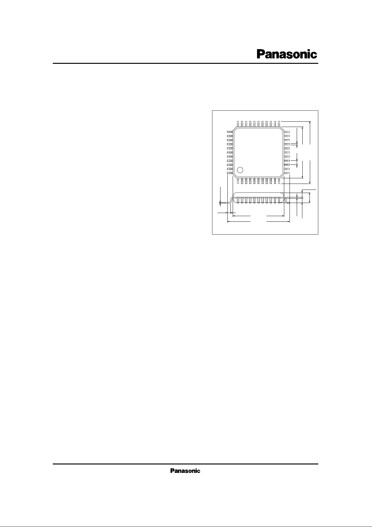
AN8819NFB
4Ch. Linear Driver IC + DC-DC Converter Control for CD
Unit : mm
111
12
22
33 23
44
34
0.3
+ 0.1
– 0.05
0.8
10.0±0.3
12.2±0.4
12.2±0.4
10.0±0.3
(0.6)
0.1±0.1
2.0±0.3
0.9±0.1
0.9±0.1
0.2
+ 0.1
– 0.05
44-lead QFP package (QFP044-P-1010)
Page 2
AN8819NFB
ICs for CD/CD-ROM Player
■ Block Diagram
BTL BTL BTL BTL
+
–
+
–
+
–
26 25 24 23 29 30 31 32 28 27 6 357
43
44
15 16 17 18 19 20 21 22
34 33
42
+
–
+
–
+
–
36 37 39 41 9
38
1
40
3
13 12 11 5 4 8 2
POWER
OFF
+
–
+
–
+
–
14
10
PWM
+– +– +– +–
+–
Max.
Value
Absolute
Value
Ripple
Filter
DC-DC Conv.
Switching
Circuit
Starter exchange
Initial setting
Thermal
Shutdown
Starter
Absolute
Value
Absolute
Value
Absolute
Value
DRV
CC
SV
CC
PGND
SGND
PV
CC
Page 3
ICs for CD/CD-ROM Player
AN8819NFB
■ Pin Description
Pin No.
Pin Name
1
2
3
4
5
6
7
8
9
10
11
12
13
14
15
16
17
18
19
20
21
22
PV
CC
Supply Pin
DED Dead Time Input Pin
OUT DC-DC Converter Output Pin
FB Error Amp. Input Pin
IN Error Amp. Output Pin
DRGND Ground Pin
SGND Ground Pin
SPRO Short-Circuit Protection Input Pin
BSEL Empty Detection Level Changeover Pin
V
SEN
Empty Detection Input Pin
SV
CC
Power Pin
CRIP Capacitor Pin for Ripple Rejection
AVDD Ripple Filter Ouput Pin
DRV
CC
Supply Pin
V
REF
1/2 VCC Input Pin
INFO Driver Input Pin
INTR Driver Input Pin
LDON Driver ON – OFF Control Pin
INSP Driver Input Pin
PC Driver ON – OFF Control Pin
INTV Driver Input Pin
TRVSTOP Driver ON – OFF Control Pin
Pin No.
Pin Name
23
24
25
26
27
28
29
30
31
32
33
34
35
36
37
38
39
40
41
42
43
44
TR– Driver Output Pin
TR+ Driver Output Pin
FO – Driver Output Pin
FO + Driver Output Pin
PGND Ground Pin
PGND Ground Pin
SP + Driver Output Pin
SP – Driver Output Pin
TV+ Driver Output Pin
TV– Driver Output Pin
VC Driver Power Voltage Pin
TB PWM Circuit Output Pin
RESET Reset Output Pin
MRST Muting Reset Output Pin
EMP Empty Detection Output Pin
CLK External Synchronization Input Pin
START Start Oscillation Start Input Pin
POWER Power On/Off Input Pin
CT Triangular Wave Oscillation Pin
PWMG PWM Loop Gain Adjustment Pin
COMPO APC Comparator Output Pin
COMPI APC Comparator Input Pin
■ Absolute Maximum Ratings (Ta=25˚C)
PV
CC
SV
CC
DRV
CC
V
10max.
V
33max.
I
CC
P
D
T
opr
T
stg
Supply Voltage
V
SEN
Pin Maximum Applied Voltage
V
C
Pin Maximum Applied Voltage
Supply Current
Power Dissipation
Note)
Operating Ambient Temperature
Storage Temperature
V
V
V
mA
mW
˚C
˚C
Parameter Symbol Rating Unit
15
6
6
15
9
880
–25 ~ + 75
–55 ~ + 125
Note) Unit
■ Recommended Operating Range (Ta=25˚C)
Parameter Symbol Range
Operating Supply Voltage Range
PV
CC
SV
CC
DRV
CC
1.5V ~ 9V
2.7V ~ 5.5V
2.7V ~ 5.5V
Page 4
AN8819NFB
ICs for CD/CD-ROM Player
Parameter Symbol Condition min. typ. max. Unit
■ Electrical Characteristics (Ta=25˚C±2˚C)
Driver Portion
V
DMAX
I
DMAX
G
+
G
sp +
V
OFF
V
SPOFF
I
DZ
I
SpDZ
V
mA
kΩ
kΩ
mV
mV
µA
µA
2.0
1.8
1.8
4.5
3.0
5.1
2.0
43
87
SVCC No Load Supply Current
DRVCC No Load Supply Current
PVCC No Load Supply Current
PVCC Leak Current
I
11Q
I
14Q
I
1Q
I
1L
PV
CC
= 2.4V, SV
CC
= DRV
CC
= 3.2V, V
REF
= 1.6V
3.1
2.4
2.6
mA
mA
mA
µA
500
33
67
–50
–100
–1
–2
DRV
CC
–1.2
53
107
50
100
1
2
Maximum Drive Voltage
of Pins FO, TR, SP and TV
Ripple Rejection Ratio
R
R13
40
dB
PV
CC
= 4V,
SV
CC
= DRV
CC
= 3.2V
PV
CC
= 4V,
SV
CC
= DRV
CC
= 3.2V
PV
CC
= 4V,
SV
CC
= DRV
CC
= 3.2V
PV
CC
= 4V,
SV
CC
= DRV
CC
= 3.2V
PV
CC
= 4V,
SV
CC
= DRV
CC
= 3.2V
PV
CC
= 4V,
SV
CC
= DRV
CC
= 3.2V
PV
CC
= 4V,
SV
CC
= DRV
CC
= 3.2V
DC-DC Converter Portion
%
%
%
V
V
kHz
kHz
74
80
45
1.5
0.3
83
65
PV
CC
= 2.4V, SV
CC
= DRV
CC
= 3.2V, CT = 390pF/470kΩ,
V
IN
= 0.8V
65
74
35
1.08
0.15
60
54
83
86
55
1.71
0.4
115
76
PV
CC1
= 2.4V, SV
CC
= DRV
CC
= 3.2V, V
REF
= 1.6V
PV
CC1
= 2.4V, SV
CC
= DRV
CC
= 3.2V, V
REF
= 1.6V
PV
CC
= 9V, SV
CC
= DRV
CC
= 0V, V
ERF
= 0V
Maximum Drive Current
Focus/Tracking/Traverse
Transmission Gain (+)
Spindle Transmission Gain (+)
Focus/Tracking/Traverse
Output Offset Voltage
Spindle Output Offset Voltage
Focus/Tracking/Traverse
Input Conversion Dead Zone
Spindle Input Conversion Dead Zone
PV
CC
= 4V,
SV
CC
= DRV
CC
= 3.2V
D
2C
D
2F
D
2S
V
20H
V
20L
F
41S
F
41F
PV
CC
= 2.4V, SV
CC
= DRV
CC
= 3.2V, CT = 390pF/470kΩ,
V
IN
= 0.8V
PV
CC
= 2.4V, SV
CC
= DRV
CC
= 3.2V, CT = 390pF/470kΩ,
V
IN
= 0.8V
PV
CC
= 2.4V, SV
CC
= 3.2V
I
OUT
= –25mA,
V
CT
= 0V, V
FB
= 0.7V
PV
CC
= 2.4V, SV
CC
= DRV
CC
= 3.2V, I
OUT
= 15mA,
V
CT
= 1V, V
FB
= 0.5V
PV
CC
= 3.2V, SV
CC
= 0V
CT
= 390pF/470kΩ
PV
CC
= 2.4V, SV
CC
= DRV
CC
= 3.2V, CT = 390pF/470kΩ
PV
CC
= 2.4V, SV
CC
= DRV
CC
= 3.2V, Input = 35mVrms/20kHz
Ripple Filter Portion
CLK Synchronization Output Pulse
Maximum Duty
Self-Running Output Pulse
Maximum Duty
Starting Output Pulse Maximum Duty
Self-Running Output Voltage (H)
Self-Running Output Voltage (L)
Starting Oscillation Frequency
Self-Running Oscillation Frequency
Page 5

ICs for CD/CD-ROM Player
AN8819NFB
■ Pin Description
Pin Description Equivalent Circuit
Pin No.
11
7
14
6
1
Symbol I/O
27
28
2
3
SV
CC
SGND
DRV
CC
DRGND
PV
CC
PGND
DED
OUT
I
I
I
I
I
I
O
Supply pin for control circuits
other than of driver, not connected
with DRVCC, PV
CC
Ground pin for control circuits
other than of driver
Supply pin for control circuit of
driver, not connected with SV
CC
,
PV
CC
Ground pin for control circuit of
driver
Supply pin supplying the current
for output power transistor
Ground pin for output power
transistor
Setting pin for dead time control
input and soft start
Switching output pin
11
7
14
1
2
6
27
28
50kΩ
200Ω
15kΩ
25kΩ
SV
CC
3
PV
CC
Page 6

AN8819NFB
ICs for CD/CD-ROM Player
■ Pin Description (Cont.)
Pin Description Equivalent Circuit
Pin No.
4
5
Symbol I/O
8
40
13
12
FB
IN
SPRO
POWER
AVDD
CRIP
O
I
I
I
O
Error amp. output pin
Error amp. input pin
Short-circuit protection input pin
Switching output ON/OFF pin
Supply pin for D/A converter
External capacitor pin for ripple
rejection
5
8
40
4
SV
CC
SV
CC
26.9kΩ
13.1kΩ
16.4kΩ
22kΩ
20kΩ
79kΩ
62kΩ
32kΩ
13
12
SV
CC
SV
CC
Page 7

ICs for CD/CD-ROM Player
AN8819NFB
■ Pin Description (Cont.)
Pin Description Equivalent Circuit
Pin No.
15
Symbol I/O
Power cut input pin for Drivers
FO, TR.
Driver output at L = GND
16
17
19
21
18
20
22
23
24
25
26
30
29
32
31
33
V
REF
INFO
INTR
INSP
INTV
LDON
PC
TR–
TR+
FO –
FO +
SP –
SP +
TV–
TV+
VC
TRV
STOP
I
I
I
I
I
I
I
I
O
O
O
O
O
O
O
O
O
V
REF
input pin
Input pin for Driver FO
Input pin for Driver TR
Input pin for Driver SP
Input pin for Driver TV
Power cut input pin for Driver SP.
Driver output at H = GND
Power cut input pin for Driver TV.
Driver output at H = GND
15
DRV
CC
DRV
CC
DRV
CC
100kΩ
1kΩ
1kΩ
40kΩ
80kΩ
DRV
CC
86kΩ
86kΩ
16
17
or
18
20
33
22
or
19
or
21
or
24 26
or
31
or
or
29
23 25
or
32
or
or
30
V
REF
– output pin of Driver TR
+ output pin of Driver TR
– output pin of Driver FO
+ output pin of Driver FO
– output pin of Driver SP
+ output pin of Driver SP
– output pin of Driver TV
+ output pin of Driver TV
Driver supply pin
Page 8

AN8819NFB
ICs for CD/CD-ROM Player
■ Pin Description (Cont.)
Pin Description Equivalent Circuit
Pin No.
9
Symbol I/O
Battery shortage detection output
pin for battery voltage detection
circuit
Reset output pin.
Reset voltage = Output voltage ×
90%
10
37
39
35
36
BSEL
V
SEN
EMP
START
MRST
RESET
Pin switching the dry cell and
charger battery for battery voltage
detection circuit
Battery voltage detection input pin
for battery voltage detection circuit
Muting reset output pin.
Reset voltage = Output voltage ×
90%
Start pin.
OUT pin starts switching in start
mode
9
PV
CC
30kΩ
7.8kΩ
9.9kΩ
7kΩ
70kΩ
10
37
35
36
PV
CC
39
PV
CC
PV
CC
200kΩ
100kΩ
PV
CC
20kΩ
60kΩ
40kΩ
I
I
I
O
O
O
Page 9

ICs for CD/CD-ROM Player
AN8819NFB
■ Pin Description (Cont.)
Pin Description Equivalent Circuit
Pin No.
Symbol I/O
Clock input pin, used to synchronize the triangular wave oscillation
with clock.
38
41
34
42
43
44
CLK
CT
TB
PWMG
COMP0
COMP1
I
O
O
O
I
Triangular wave oscillation pin.
Oscillation frequency determined
by external R and C.
Recommendable values : 470kΩ,
390pF
Transistor base pin for controlling
the driver supply voltage PWM
Gain adjustment pin for controlling
the driver supply voltage PWM
APC switching comparator output
pin
APC switching comparator input
pin
38
50kΩ
20kΩ
50kΩ
160kΩ
41
34
PV
CC
60kΩ
42
DRV
CC
43
44
SV
CC
1kΩ
Page 10

AN8819NFB
ICs for CD/CD-ROM Player
■ Characteristic Curve
2,000
1,800
1,600
1,400
1,200
1,000
800
600
400
200
0
Ambient Temperature Ta (˚C)
Power Dissipation P
D
(mW)
250 75 125
Glass epoxy board
(50mm × 50mm × 0.8mm)
Rthj– a = 70˚C/W
P
D
=1786mW (25˚C)
15010050
1,786
880
Unit
Rthj– a = 142˚C/W
PD = 880mW (25˚C)
PD –Ta
■ Description for use
• Driver Portion
Set the driver gain calculated by the equation shown below, except for SP driver. For SP driver, the gain must be set to the
calculated value + 6dB.
G =
43kΩ
1.0kΩ + R
The total channel driver supply is Pin33.
Set the driver supply as necessary, since the output amplitude increases with increase of the supply voltage. However, also
increase the voltage of DRVCC pin (Pin14) at the same time.
As protection functions, V
REF
detection and heat protection circuits are incorporated.
V
REF
detector sets the driver output to high impedance, when the voltage applied to V
REF
is 0.75V or less.
For the heat protective circuit, the set temperature for operation is approx. 150˚C and the release temperature is approx. 120˚C.
FO and TR drivers have the built-in function for making short-circuit between either loading end and GND by LDON (Pin18),
and for SP and TV drivers by PC (Pin20) and TRVSTOP (Pin22).
LDON : Output GND at L
PC : Output GND at H
TRVSTOP : Output GND at H
R : External input resistance
Page 11

ICs for CD/CD-ROM Player
AN8819NFB
R2
R3
IC Inside
10
–
+
37
1.25V
EMP
V
SEN
’
R1
V
SEN
–
+
4
11
5
SV
CC
R1
R2
IN
R3
R4
1.11V
FB
• DC-DC Converter Portion
3.4V regulator can be constructed by using external components. The output voltage can be made variable by using an external
resistance.
The short-circuit protective function stops switching of OUT pin (Pin3), unless the output of error amplifier (Pin4) reaches L
after H, within t = C
SPRO
× VTH/I
SPRO
(V
TH
= 1.1V I
SPRO
= 30µA). (It is recommended that an electrolytic capacitor of 4.7µF
around should be used for Pin3.)
The soft start function works by attaching a capacitor to Pin2 for GND. t = C
DED
× R (R = 60kΩ)
Also, MAX duty can be changed by attaching an external resistance to Pin2. The output voltage is determined as follows:
(Example)
Assuming R1 + R2 = 50kΩ
R1 × R3
+
R2 × R4
R1 + R3 R2 + R4
SVCC = 1.1 ×
R2 × R4
R2 + R4
Where
R3 = 26.9kΩ
R4 = 13.1kΩ
• Ripple Filter Portion for DA Converter (Ripple Filter of Low Saturation Voltage Type)
Attach a capacitor for noise removal to CRIP pin for GND.
(A capacitor of 22µF around is recommended.) Output current : 10mA (typ.)
• Battery Voltage Detection Circuit
The voltage applied to V
SEN
pin (Pin10) and the constant voltage are compared for output to EMP pin (Pin37).
There is approx. 50mV of hysteresis from detection to reset to prevent the output chattering.
The detection threshold voltage can be made variable by an external resistance.
The threshold values with no external resistances at V
SEN
pin (Pin10) are as follows:
Detection : V
SEN
= 2.2V (typ.) BSEL (Pin9) = L
Reset : V
SEN
= 2.25V (typ.) BSEL (Pin9) = L
Detection : V
SEN
= 1.8V (typ.) BSEL (Pin9) = HiZ
Reset : V
SEN
= 1.85V (typ.) BSEL (Pin9) = HiZ
Use the following equation as reference to determine the detection threshold voltage:
Assuming that the voltage of V
SEN
(Pin10) at battery
shortage detection is V
SEN
’
V
SEN
’ =
R1 + R2 + R3
× 1.25
R3
Where R1 : External Resistance
R2 : 8.0kΩ
R3 : 16.5kΩ (BSEL = HiZ)
R3 : 10.5kΩ (BSEL = L)
• RESET and MRST Portions
RESET (Pin35) is changed from L to H, and MRST pin is changed from H to L, with approx. 90% of the output voltage by a DCDC converter.
IC Inside
 Loading...