

Page 1
ICs for Optical Disk Drive
AN8737SB
3-channel driver IC for optical disk drive
■ Overview
The AN8737SB is a BTL type 3-channel driver
IC, adopting a current feedback system for 2 channels, which makes it optimum for an actuator and a
motor driver of CD-ROM/DVD-ROM. It can also
constitute an optimum system in combination with
the AN8488SB, a spindle plus loading driver IC. A
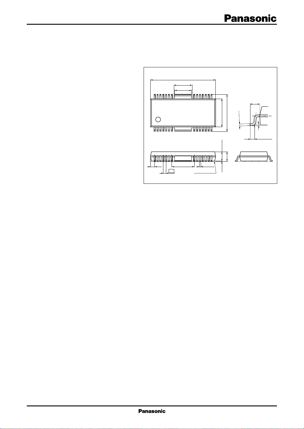
surface mount-type package of good heat radiation
characteristic is used.
■ Features
• Little phase delay due to a current feedback system
(2 channels for actuator)
• The remaining channel is available for either
traverse or loading motor drive.
• Wide output dynamic range (4 V/I
= 800 mA)
O
• Standby function built in (all channels can be
muted.)
• Thermal shut-down circuit built in
• With thermal flag pin
■ Applications
• CD/CD-ROM player
• DVD/DVD-ROM drive
18.4±0.2
(5.15)
28 22 21
17 814
(1.2)
(4.8)
(6.4)
0.8
15
8.3±0.22.7±0.20.1±0.1
+0.10
0.35
–0.05
Seating plane
HSOP042-P-0400
+0.10
10.93±0.30
Unit: mm
(1.315)
–0.05
0.30
0° to 10°
0.65±0.20
1
Page 2
AN8737SB ICs for Optical Disk Drive
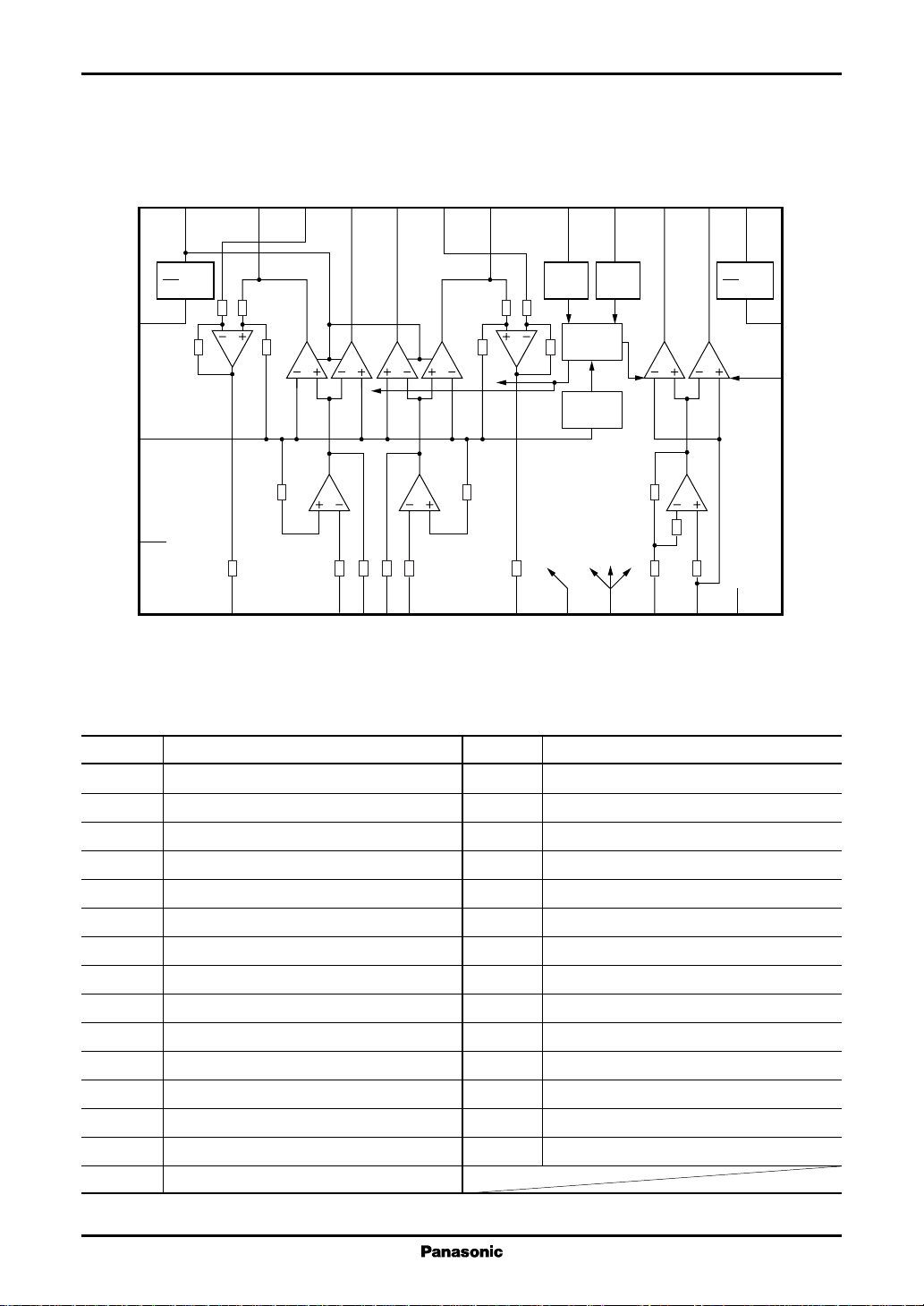
■ Block Diagram
PGND1
V
REF
N.C.
13
26
10
CC1
VO1−
5
VS1
12
VO1+
VO2+
VS2
VO2−
15
28
14
PV
8
1
V
CC
2
9
V
det.
7
CC
CC
SV
TFLG
20
Temp.
det.
16
CC2
VO3−
VO3+
PV
19
21
1
V
CC
2
17
PGND2
Reset
18
PC2
V
REF
reset
6
VRB1
3
IN1
4
OUT1
1
OUT2
2
IN2
27
VFB2
11
PC1
24
SB
23
IN3N
25
IN3P
Fin
SGND
■ Pin Descriptions
Pin No. Description
1 Ch. 2 first stage feedback pin
2 Ch. 2 first stage input pin
3 Ch. 1 first stage input pin
4 Ch. 1 first stage feedback pin
5 Ch. 1 current feedback input pin
6 Ch. 1 current feedback output pin
7 Control side power supply pin
8 Ch. 1 & ch. 2 power side power supply pin
9 Ch. 1 reverse direction output pin
10 N.C.
11 Ch. 1 & Ch. 2 mute pin
12 Ch. 2 forward direction output pin
13 Ch. 1 & ch. 2 power side grounding pin
14 Ch. 2 reverse direction output pin
15 Ch. 2 forward direction output pin
Pin No. Description
16 Ch. 3 reverse direction output pin
17 Ch. 3 power side grounding pin
18 Ch. 3 mute pin
19 Ch. 3 forward direction output pin
20 TDS flag pin
21 Ch. 3 power side power supply pin
22 N.C.
23 Ch. 3 reverse rotation input pin
24 Standby input pin
25 Ch. 3 forward rotation input pin
26 Reference voltage input pin
27 Ch. 2 current feedback output pin
28 Ch. 2 current feedback input pin
Fin Control side grounding pin
2
Page 3

ICs for Optical Disk Drive AN8737SB
■ Absolute Maximum Ratings
Parameter Symbol Rating Unit
Supply voltage V
Supply voltage range SVCC , PV
2
Supply current
Power dissipation
Operating ambient temperature
Storage temperature
Note)*1: Except for the operating ambient temperature and storage temperature, all ratings are for Ta = 25°C.
2: I
*
PVCC1
3: Use within the range of PD = 542 mW or less at Ta = 85°C, following the allowable power dissipation characteristic curve
*
of "■ Application Notes".
*
3
*
1
*
1
*
be 1 A or less for channel 1 and channel 2, respectively.
I
SVCC
I
PVCC1
I
PVCC2
P
T
T
CC
CC1
D
opr
stg
, PV
CC2
■ Recommended Operating Range
Parameter Symbol Range Unit
Supply voltage SV
PV
CC1
CC
, PV
CC2
14.0 V
− 0.3 to +14.0 V
500 mA
2.0 A
800 mA
542 mW
−30 to +85 °C
−55 to +150 °C
4.5 to 13.5 V
3.5 to 13.5
■ Electrical Characteristics at SVCC = 12 V, PV
VSB = V
PC1
= V
= 3.3 V, V
PC2
IN1
= V
IN2
= V
IN3
= 5 V, PV
CC1
= 5 V, RL = 8 Ω, V
CC2
= 1.65 V, Ta = 25°C
= 1.65 V,
REF
Parameter Symbol Conditions Min Typ Max Unit
= V
= V
, V
Current consumption 1 I
(no signal) VSB = V
Current consumption 2 I
(no signal) VSB = V
Current consumption 1 I
(standby) VSB = V
Current consumption 2 I
(standby) VSB = V
SVOVIN1
PVOVIN1
SVSBVIN1
PVSBVIN1
= V
= V
= V
IN2
PC1
IN2
PC1
IN2
PC1
IN2
PC1
= V
= V
= V
= V
= V
= V
= V
PC2
PC2
PC2
PC2
Driver 1, Driver 2 RL1 , RL2 = 4 Ω, RS1 , RS2 = 0.5 Ω, R
Output offset voltage V
OF1VIN
Gain (+)G1+ VIN = V
= V
REF
±50 mV 9 11 13 dB
REF
REF
REF
REF
REF
IN1
= 2.5 V 25 45 mA
IN3P
= 3.3 V
, V
= 2.5 V 25 45 mA
IN3P
= 3.3 V
, V
= 2.5 V 0.6 1.5 mA
IN3P
= 0 V
, V
= 2.5 V 0.2 1.0 mA
IN3P
= 0 V
, R
= 10 kΩ, RF1 , RF2 = 4.3 kΩ
IN2
−100 0 100 mV
Relative gain (+/−)G1 −1.5 +1.5 dB
Maximum output amplitude (+)V
L1+VIN
= 3.3 V, RL1 , RL2 = 4 Ω 3.65 4.0 V
RS1 , RS2 = 0.5 Ω
Maximum output amplitude (−)V
L1−VIN
= 0 V, RL1 , RL2 = 4 Ω−4.0 −3.65 V
RS1 , RS2 = 0.5 Ω
3
Page 4

AN8737SB ICs for Optical Disk Drive
■ Electrical Characteristics at SVCC = 12 V, PV
VSB = V
PC1
= V
= 3.3 V, V
PC2
IN1
= V
IN2
= V
IN3
= 5 V, PV
CC1
= 5 V, RL = 8 Ω, V
CC2
= 1.65 V, Ta = 25°C (continued)
= 1.65 V,
REF
Parameter Symbol Conditions Min Typ Max Unit
Driver 3 RL = 8 Ω
Output offset voltage V
OF3VIN3P
Gain (+)G3+ V
= V
= 2.5 V, V
IN3P
= 2.5 V −150 0 150 mV
IN3N
= 2.5 V±50 mV 19 20.5 22 dB
IN3P
No external resistor
Relative gain (+/−)G3 −1.5 +1.5 dB
V
Output voltage (+)V
3+
= 5 V, 3.05 3.4 3.75 V
IN3N
RA1 = 27 kΩ, RA2 = 6.8 kΩ
Output voltage (−)V
V
3−
= 0 V, −3.75 −3.4 −3.05 V
IN3N
RA1 = 27 kΩ, RA2 = 6.8 kΩ
Input pin bias current I
IN3
V
= 0 V 1 µA
IN3N
Standby operation High: Active, low or Hi-Z: Standby
High-level SB threshold voltage V
Low-level SB threshold voltage V
SB input current I
SVCC = 12 V 2.6 V
SBH
SVCC = 12 V 0.7 V
SBL
VSB = 5 V 50 120 µA
SB
Power cut operation High: Active, low or Hiz: Power cut
High-level PC1 threshold voltage V
Low-level PC1 threshold voltage V
High-level PC2 threshold voltage V
Low-level PC2 threshold voltage V
PC1 input current I
PC2 input current I
SVCC = 12 V 2.6 V
PC1H
SVCC = 12 V 0.7 V
PC1L
SVCC = 12 V 2.6 V
PC2H
SVCC = 12 V 0.7 V
PC2L
V
PC1
PC2
= 5 V 70 120 µA
PC1
V
= 5 V 70 120 µA
PC2
Reset current
Reset operation release supply V
RST
4.5 V
voltage
V
detection voltage V
REF
R
1.20 V
• Design reference data
Note) The characteristics listed below are theoretical values based on the IC design and are not guaranteed.
Parameter Symbol Conditions Min Typ Max Unit
Thermal protection circuit
Operating temperature T
THD
160 °C
equilibrium value
Operating temperature ∆T
THD
40 °C
hysteresis width
Temperature flag balancing T
FLG
150 °C
value
Temperature flag hysteresis ∆T
FLG
20 °C
width
4
Page 5

ICs for Optical Disk Drive AN8737SB
■ Electrical Characteristics at SVCC = 12 V, PV
VSB = V
PC1
= V
= 3.3 V, V
PC2
IN1
= V
IN2
= V
IN3
= 5 V, PV
CC1
= 5 V, RL = 8 Ω, V
CC2
= 1.65 V, Ta = 25°C (continued)
• Design reference data (continued)
Note) The characteristics listed below are theoretical values based on the IC design and are not guaranteed.
Parameter Symbol Conditions Min Typ Max Unit
Thermal protection circuit (continued)
Operating temperature difference bet.
∆T
TF
10 °C
thermal protection/temperature flag
Temperature flag output high V
SVCC = 12 V 5 V
FLH
value
Supply voltage detection hysteresis ∆V
HD
0.2 V
width
■ Usage Notes
1. Use SVCC at the maximum potential.
Otherwise it will cause operation error.
2. Do not use PV
3. Driver 1, driver 2 gain setting
(Use a resistor of sufficient power dissipation for RS .)
CC1
and PV
at 2 V or less, or at the high impedance.
CC2
R
E
C
E
= 1.65 V,
REF
Input
R
V
IN
pin
IN
R
FB
6 or 27
3 or 2
500 Ω
500 Ω
V
REF
200 Ω
V
REF
V
REF
4. On the mode of mute:
SB = PC1 = high
PC2 = high PC2 = low or Hi-Z
Ch. 1, Ch. 2 Active Active All mute,
Ch. 3 Active Mute power save
Never fail to input the same signal into SB pin (pin 24) and PC1 pin (pin 11).
4 or 1
Forward
rotation pin
× 5
12 or 15
× 5
9 or 14
Pwr. amp.
5 or 28
Reverse
rotation pin
SB = PC1 = low or Hi-Z
4 Ω
0.5 Ω
R
L
R
S
5
Page 6

AN8737SB ICs for Optical Disk Drive
■ Usage Notes (continued)
5. On the output maximum amplitude (Reference data: typical value)
5.0
4.5
4.0
3.5
Output maximum amplitude (V)
3.0
0.4
0.6 0.8 1.0 1.1
Load current (A)
Use load current at 1 A or less.
6 Appropriate care should be taken on the characteristics.
When changing an external circuit constant on actual use, secure an appropriate margin in consideration of characteristic fluctuation of external parts and our ICs including transient characteristics as well as static ones.
7 Avoid the short-circuits between output pin or current detection pin and VCC (line-to-supply fault), output pin or
current detection pin and GND (line-to-ground fault), and output pins or output pin and current detection pin (load
short-ciruit).
8 An appropriate prior study should be done for use of dip soldering.
9 Care should be taken on use of the following pin because of its low static breakdown voltage (C = 200 pF, R = 0 Ω).
Pin 18: Breakdown at 200 V
6
Page 7

ICs for Optical Disk Drive AN8737SB
■ Application Notes
• PD Ta curves of HSOP042-P-0400
T
P
D
a
2.500
2.240
(W)
D
Power dissipation P
2.000
1.500
1.042
1.000
0.500
Independent IC
without a heat sink
= 119.9°C/W
R
th(j-a)
Mounted on standard board
(glass epoxy:
75 mm × 75 mm × t1.6 mm)
= 55.8°C/W
R
th(j-a)
0.000
0 25 50 75 100 125
Ambient temperature Ta (°C)
150
7
Page 8

AN8737SB ICs for Optical Disk Drive
■ Application Circuit Example
PGND1
V
REF
1.65 V
N.C.
5 V
13
26
10
Snubber
R
R
S1
VS1
5
L1
4.0 Ω
0.5 Ω
CC1
PV
8
1
V
CC
2
VO1−
9
Snubber
R
R
L2
0.5 Ω
VS2
S2
4.0 Ω
VO1+
VO2+
121152282714
12 V
R
VO3−
L2
8.0 Ω
VO3+
High: High
temp.
CC
VO2−
SV
TFLG
19
V
Temp.
CC
det.
det.
5 V
CC2
PV
21
1
V
CC
2
PGND2
17
Reset
18
V
REF
reset
PC2
6
3
VRB1
4.3 kΩ
IN1
4.7 kΩ
R
= 10 kΩ
560 pF
IN2
4
OUT1
OUT2
560 pF
4.7 kΩ
IN2
4.3 kΩ
R
IN2
= 10 kΩ
1172420231625
PC1
VFB2
High: Active
Low : All mute
power save
SB
6.8 kΩ
27 kΩ
IN3N
Fin
SGND
IN3P
8
 Loading...