

Page 1
ICs for Compact Disc/CD-ROM Player
AN8730SB
4-channel driver IC for optical disk
■ Overview
The AN8730SB is a 4-channel driver IC, which can
operate in a low voltage, employing the low power consumption type H-bridge system with a switching regulator. It is especially suited for a portable CD/MD player.
■ Features
• Low power consumption due to PWM control of power
supply
• Wide output D-range independent of the reference volt-
age of the system
• Enable to set input/output gain by an external resistor
• Independent power on/off for 2 channels and simulta-
neous on/off for other 2 channels as well
• Battery voltage detection circuit built-in
• Thermal shut-down circuit (with hysteresis) built-in
■ Applications
• Portable CD/MD
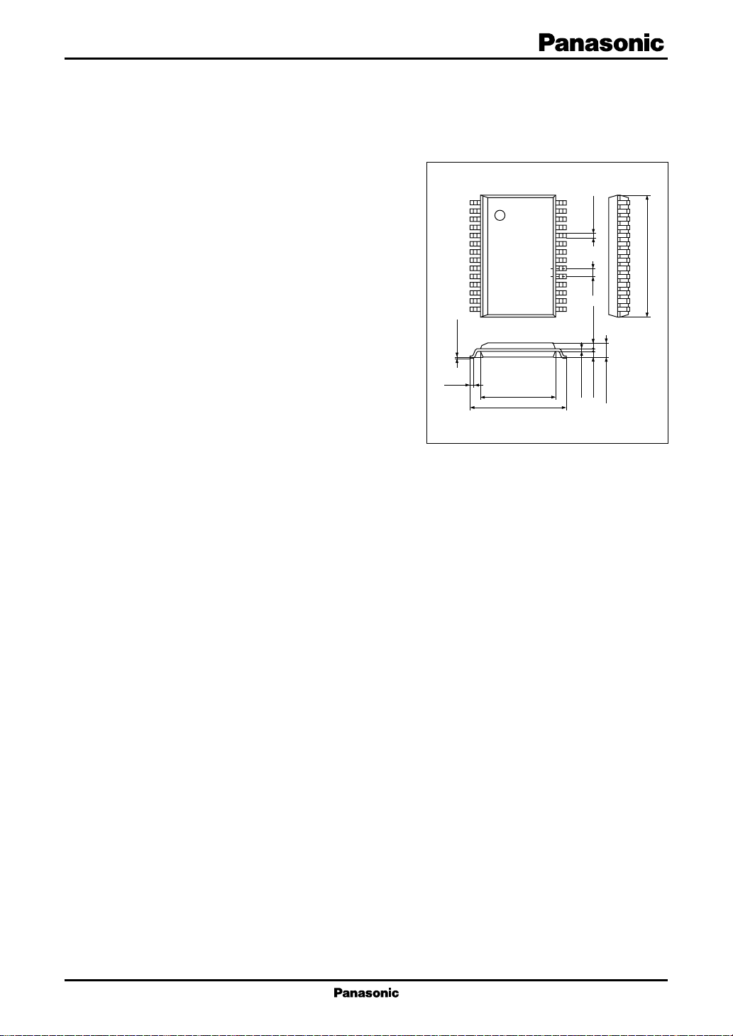
14
0.1±0.1
(0.4)
1
28
15
+0.1
7.2±0.3
9.3±0.3
SSOP028 P-0375A
–0.05
0.2
Unit: mm
0.3±0.1
0.8
0.9±0.1 0.9±0.1
2.05±0.2
11.6±0.3
1
Page 2
AN8730SB ICs for Compact Disc/CD-ROM Player
■ Block Diagram
STNBY
12
SGND
PGND
8
21
25
24
23
22
19
20
BTL
BTL
BTL
Power
cut
Absolute
value
Absolute
value
Absolute
value
Thermal
shut-down
V
REF
detection
3
TRVSTOP
4
INTV
6
5
INSP
10
LDON
9
INFO
PC
17
BTL
18
V
TB
CT
Absolute
value
27
C
PWM
26
7
Triangular
Maximum
value
wave
2
28
CLK
PWMG
1
CC
PV
13
CC
SV
11
14
15
16
INTR
V
REF
V
SEN
EMP
2
Page 3

ICs for Compact Disc/CD-ROM Player AN8730SB
■ Pin Descriptions
Pin No. Symbol Description
1PVCCSupply voltage pin
2 CLK External sync. input pin
3 TRVSTOP Driver on-off control pin
4 INTV Driver input pin
5 INSP Driver input pin
6 PC Driver on-off control pin
7 CT Triangular wave oscillation pin
8 SGND Ground pin
9 INFO Driver input pin
10 LDON Driver on-off control pin
11 INTR Driver input pin
12 STNBY Standby mode input pin
13 SV
14 V
Supply voltage pin
CC
V
REF
input pin
REF
Pin No. Symbol Description
15 V
Empty detection input pin
SEN
16 EMP Empty detection output pin
17 TR− Driver output pin
18 TR+ Driver output pin
19 FO− Driver output pin
20 FO+ Driver output pin
21 PGND Ground pin
22 SP+ Driver output pin
23 SP− Driver output pin
24 TV+ Driver output pin
25 TV− Driver output pin
26 TB PWM circuit output pin
27 V
Drive supply voltage pin
C
28 PWMG PWM loop gain adjustment pin
■ Absolute Maximum Ratings
Parameter Symbol Rating Unit
Supply voltage PV
Supply voltage range PV
Supply current I
Supply current 1 I
Supply current 2 I
Drive output current I
2
Power dissipation
Max. application voltage to V
Operating ambient temperature
Storage temperature
Note) 1. Do not apply external currents or voltages to any pins not specifically mentioned.
For circuit currents, '+' denotes current flowing into the IC, and '−' denotes current flowing out of the IC.
1: Except for the operating ambient temperature and storage temperature, all ratings are for Ta = 25°C.
2. *
2: Ta = 75°C. For the independent IC without a heat sink. Refer to "■ Application Note" at mounting on PCB.
*
*
pin V
SEN
1
*
1
*
SV
V
SV
SVCC
PVCC
P
10max
T
T
CC
CC
C
CC
CC
CC
O
D
opr
stg
15 V
6
9
− 0.3 to +15.0 V
− 0.3 to +6.0
mA
50 mA
100 mA
500 mA
345 mW
15.0 V
−25 to +75 °C
−55 to +125 °C
■ Recommended Operating Range
Parameter Symbol Range Unit
Supply voltage PV
SV
CC
CC
2.7 to 14.0 V
2.7 to 5.5
3
Page 4

AN8730SB ICs for Compact Disc/CD-ROM Player
■ Recommended Operating Range
Parameter Symbol Range Unit
Supply voltage PV
SV
CC
CC
■ Electrical Characteristics at SVCC = PVCC = 5 V, Ta = 25°C
Parameter Symbol Conditions Min Typ Max Unit
<Common block>
Supply current of SVCC at no load I
In standby mode I
supply current of SVCC at no load STNBY = 0 V
Supply current of PVCC at no load I
VC leak current I
Free-run oscillation frequency f
at CT pin
CKL pin block
CLK pin input threshold V
CLK pin input threshold V
THH
THL
V
V
Empty detection block
EMP pin detection voltage V
Hysteresis width from EMP pin V
empty detection to recovery
EMP pin output voltage V
V
pin input resistance R
SEN
<Driver block>
Focus
Transfer gain '+'GF+ V
'+' / '−' transfer gain relative ratio G+/G− V
Dead zone converted to INFO pin input
IDZFO V
INFO pin input internal resistance R
Output offset voltage V
Max. output amplitude '+'V
Max. output amplitude '−'V
LDON pin high-level threshold V
LDON pin low-level threshold V
pin driver on-off V
V
REF
FOOFFVREF
(OFF)
FOLM+
FOLM−
10THHVREF
10THLVREF
14THH
high-level threshold
V
pin driver on-off V
REF
14THL
low-level threshold
PVCC = SVCC = 5 V, V
13Q
PVCC = SVCC = 5 V, V
13S
PVCC = SVCC = 5 V, V
1Q
VC = 9 V 10 µA
VCL
CT = 150 pF, 470 kΩ165 kHz
3F
2THHfIN
2THLfIN
16TH1
16H
16OIEMP
15
9
= 88.2 kHz 2.0 V
= 88.2 kHz 0.8 V
= +1.0 mA, V
= 1.5 V 11.3 13.8 16.3 dB
REF
= 1.5 V −1.5 0 +1.5 dB
REF
= 1.5 V −10 0 +10 mV
REF
V
= 1.5 V, LDON = 3.0 V 0.8 1.0 1.2 kΩ
REF
= INFO = 1.6 V −50 +50 mV
PVCC = SVCC = 5 V, V
PVCC = SVCC = 5 V, V
= 1.6 V, INFO = 1.8 V 2.0 V
= 1.6 V, INFO = 1.8 V 1.0 V
INFO = 1.8 V 1.25 V
INFO = 1.8 V 0.75 V
2.7 to 14.0 V
2.7 to 5.5
= 1.5 V 4.2 7.0 mA
REF
= 1.5 V 0.8 2 mA
REF
= 1.5 V 3.4 5.5 mA
REF
1.7 1.85 1.9 V
50 80 110 mV
= 1 V 0.5 V
SEN
21.5 25 28.5 kΩ
= 1.5 V 2.5 3.4 V
REF
= 1.5 V 2.5 3.4 V
REF
4
Page 5

ICs for Compact Disc/CD-ROM Player AN8730SB
■ Electrical Characteristics at SVCC = PVCC = 5 V, Ta = 25°C (continued)
Parameter Symbol Conditions Min Typ Max Unit
<Driver block> (continued)
Tracking
Transfer gain '+' GTR+ 11.3 13.8 16.3 dB
'+' / '−' transfer gain relative ratio G+/G−−1.5 0 +1.5 dB
Dead zone converted to INTR pin input
INTR pin input internal resistance R
Output offset voltage V
Max. output amplitude '+'V
Max. output amplitude '−'V
Spindle
Transfer gain '+' GSP+ 17.5 20.0 22.5 dB
'+' / '−' transfer gain relative ratio G+/G−−1.7 −0.2 +1.3 dB
Dead zone converted to INSP pin input
INSP pin input internal resistance R
Output offset voltage V
Max. output amplitude '+'V
Max. output amplitude '−'V
PC pin threshold high-level V
PC pin threshold low-level V
Traverse
Transfer gain '+' GTV+ 11.3 13.8 16.3 dB
'+' / '−' transfer gain relative ratio G+/G−−1.8 −0.3 +1.2 dB
Dead zone converted to INTV pin input
INTV pin input internal resistance R
Output offset voltage V
Max. output amplitude '+'V
Max. output amplitude '−'V
TRVSTOP pin threshold high-level V
TRVSTOP pin threshold low-level V
PWM-comp.
TB pin sink current ability I
VC level shift V
IDZTR −10 0 +10 mV
11
TROFF
(OUT)
TRLM+
TRLM−
0.8 1.0 1.2 kΩ
−50 0 +50 mV
2.5 3.4 V
2.5 3.4 V
IDZSP −10 0 +10 mV
5
SPOFF
(OUT)
SPLM+
SPLM−
6THH
6THL
0.8 1.0 1.2 kΩ
−100 0 +100 mV
2.5 3.4 V
2.5 3.4 V
2.0 V
1.0 V
IDZTV −10 0 +10 mV
4
TVOFF
(OUT)
TVLM+
TVLM−
6THH
3THL
TB
C
V
= 1.6 V, INFO = 2.1 V 9 12 15 mA
REF
V
= 1.6 V, INFO = 1.8 V 0.32 0.52 0.62 V
REF
0.8 1.0 1.2 kΩ
−50 0 +50 mV
2.5 3.4 V
2.5 3.4 V
2.0 V
1.0 V
5
Page 6

AN8730SB ICs for Compact Disc/CD-ROM Player
■ Electrical Characteristics at SVCC = PVCC = 5 V, Ta = 25°C (continued)
• Design reference data
Note) The characteristics listed below are theoretical values based on the IC design and are not guaranteed.
Parameter Symbol Conditions Min Typ Max Unit
Temperature protection circuit
Thermal shut-down operating temperature TON 150 °C
driver operation → stop
Thermal shut-down operating temperature DT 30 °C
hysteresis width
■ Application Note
• PD Ta curves of SSOP028-P-0375A
P
T
D
a
1 600
1 400
1 282
1 200
(mW)
1 000
D
Power dissipation P
800
690
600
Independent IC
without a heat sink
400
R
P
200
0
0
Mounted on standard board
(glass epoxy: 50 × 50 × t0.8 mm
= 78°C/ W
R
th(j-a)
P
= 1 282 mW (25°C)
D
= 145°C/ W
th(j-a)
= 690 mW (25°C)
D
25 50 75 100 125 150
Ambient temperature Ta (°C)
3
)
6
Page 7

ICs for Compact Disc/CD-ROM Player AN8730SB
■ Application Circuit Example
STNBY
12
SGND
TV
SP
PGND
8
Power
cut
21
25
BTL
24
Absolute
value
23
BTL
22
Absolute
value
Thermal
shut-down
detection
V
REF
TRVSTOP
3
INTV
4
PC
6
INSP
5
FO
TR
V
TB
CT
19
LDON
BTL
10
20
Absolute
value
9
INFO
17
BTL
18
Absolute
value
27
C
Maximum
value
26
7
PWM
Triangular
wave
2
28
PWMG
1
CC
PV
13
CC
SV
11
14
15
16
INTR
V
REF
V
SEN
EMP
CLK
7
 Loading...