

Page 1

ICs for Optical Disk Drive
AN8725FH
Semiconductor laser power control IC
■ Overview
The AN8725FH is a laser driver IC that can set a laser
emitting level to a maximum precision in recording and
playback of an optical recording equipment such as PD,
and can modulate a laser light in tune with the external
signal.
■ Features
• Digital setting of playback current, peak current, bias
current and abnormal light emitting level
• Peak current and bias current can be modulated by the
external signal.
• Driving current set-up (digital set-up)
For playback: 8-bit + 4-bit (0 mA to 80 mA)
5-bit + 4-bit (0 mA to 150 mA)
For peak: 4-bit + 8-bit (0 mA to 150 mA)
For bias: 4-bit + 8-bit (0 mA to 150 mA)
• Laser output light monitoring circuit built-in
• Abnormal light emitting detecting function built-in:
Possible to set up excessive and insufficient light emitting levels with 4-bit DAC for playback and recording,
respectively.
• Supply voltage abnormality detection:
Voltage down (3.9 V or less), voltage up (6.1 V or more)
14.00±0.20
12.00±0.20
60 41
61
80
120
(1.25)
0.50
+0.10
0.18
–0.05
Seating plane
QFP080-P-1212
40
(1.25)
21
0.90±0.10
0.90±0.10
14.00±0.20
12.00±0.20
1.95±0.20
0.50±0.20
0.10±0.10
Unit: mm
(1.00)
–0.05
+0.10
0.15
0° to 10°
■ Applications
• Optical disk drive
1
Page 2
AN8725FH ICs for Optical Disk Drive
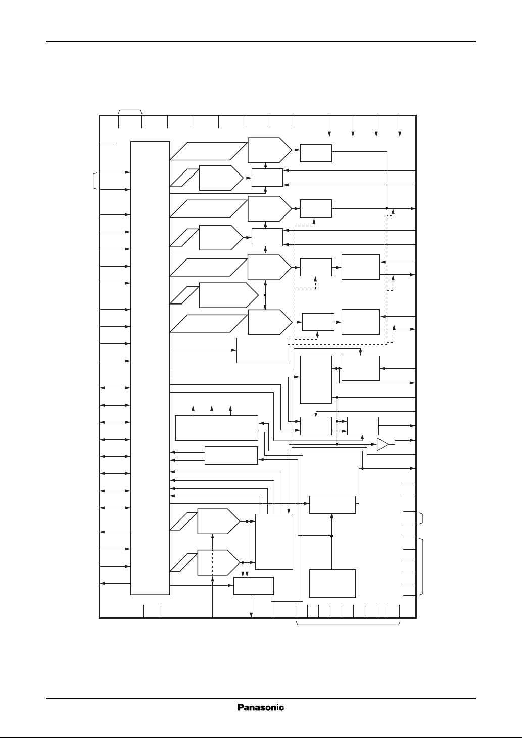
■ Block Diagram
IGND
AGND
PKMD
BIMD
RPHOLD
XWR
XRD
AD0
AD1
AD2
AD3
DT0
DT1
DT2
DT3
DT4
DT5
DT6
DT7
XLDEN
XCLR
XLDERR
XHFON
logic
CC
PKGND
PKV
72
BIV
71
77
4
Playback
current
5
DAC9
4
Playback
current
8
DAC1
8
Peak bias
4
current
DAC4
8
X1/SX2 changeover
AAF off
AAF RST
CTL SW6
DAC1
DAC9 DAC4
Current source for DAC
PS over
Supply voltage
PS down
WPW over
WPW down
RPW over
RPW down
Sleep
4
4
monitoring
Insufficient
light emission
DAC5
Excessive
light emission
DAC6
CC
LPF off
LPF off
DAC56SW
BIGND
RGND
76
62
Playback
current
DAC7
LPF9
Playback
current
DAC8
LPF1
Peak
current
DAC2
Bias
current
DAC3
Shunt circuit
SW5
Abnormal
light
emitting
detection
CC
RV
68
SW1
SW1
SW2
SW3
I/V
conversion
AAF
Sleep circuit
voltage source
BIDCP
78
Reference
(1.25 V)
PKDCP
73
64
Current
amplification
Current
amplification
Current
amplification
X1, X10
SW6
RDCP2
DAC7DAC8DAC2DAC3
Buffer
RDCP1
63
44
43
65
39
38
70
69
75
74
51
50
49
48
47
46
56
36
53
52
34
9
33
28
19
10
3
2
LPF92
LPF91
LDRP
LPF12
LPF11
XLDPK
LDPK
XLDBI
LDBI
IPD
IVIN
IVOUT
AAF
PWRMONI
DETMONI
VNR
VC
CV
CC
CGND
DV
CC
DGND
CC
AV
45
58
40
35
54
4
5
6
8
9
11
12
13
14
Control
15
16
17
18
22
23
24
25
26
27
29
32
30
31
PWMSK
ERFIL
55
ERREF
57
37
RREF
1
202141425960617980
SGND
DACMONI
2
Page 3

ICs for Optical Disk Drive AN8725FH
■ Pin Descriptions
Note) Description on notations of "Category" in the following list:
IN : Input pin I/O : Input/output pin (pull-down with 100 k Ω)
IND : Input pin (pull-down with 100 kΩ) PS : Power supply/GND pin
INU : Input pin (pull-up with 100 kΩ) MSC: Parts connecting pin, etc.
OUT: Output pin
A: Analog function D: Digital function
Pin No. Symbol Category Description
1 SGND PS D Pin connected to the chip substrate.
Must be used in the same potential as other GND pins.
2 DGND PS D GND pin exclusive for a logic circuit.
3 DGND PS D Must be used in the same potential as other GND pins.
4 PKMD IND D Peak current modulation signal input pin.
In high-level, the current set up with DAC2 is superimposed on LD.
5 BIMD IND D Bias current modulation signal input pin.
In high-level, the current set up with DAC3 is superimposed on LD.
6 RPHOLD IND D Record gate signal input pin.
Inputs a low-level in playback and a high-level in recording.
Switches an amp. of light monitoring signal, abnormally emitted light
detection level and on/off of HF module.
7 XWR INU D Register writing signal pin.
Selects a register specified by address in a fall edge and writes a bus data
on the register of the address specified in the rise edge.
8 XRD INU D Register read-out signal pin.
Register data of the address specified in low appears on the bus.
9DVCCPS D Power supply pin exclusive for a logic circuit.
Must be used in the same potential as other power supply pins.
10 DGND PS D GND pin exclusive for a logic circuit.
Must be used in the same potential as other GND pins.
11 AD0 IND D 4-bit address pin for registers.
12 AD1 IND D Selects the register to be accessed.
13 AD2 IND D
14 AD3 IND D
15 DT0 I/O D Data I/O 8-bit bus pin.
16 DT1 I/O D The bus to set the data to be written on a register and to read out the data
17 DT2 I/O D of a register.
18 DT3 I/O D
19 DGND PS D GND pin exclusive for a logic circuit.
Must be used in the same potential as other GND pins.
3
Page 4

AN8725FH ICs for Optical Disk Drive
■ Pin Descriptions (continued)
Pin No. Symbol Category Description
20 SGND PS D Pin connected to the chip substrate.
21 SGND PS D Must be used in the same potential as other GND pins.
22 DT 4 I/O D Data I/O 8-bit bus pin.
23 DT 5 I/O D The bus to set the data to be written on a register and to read out the data
24 DT 6 I/O D of a register.
25 DT 7 I/O D
26 XLDEN INU D LD enable input pin.
In a high-level or open mode, LD becomes off and open. This state is suited
to check the LD characteristics in keeping a connection to the IC. At the
time power off, both ends of LD are short-circuited by the IC for protection.
In the low-level, it returns to a normal operation.
27 XCLR IND D Clear signal input pin.
Sets an LDDENB register to "0" in the low-level and presets the status of
each DAC and each switch to an initial state as defined separately.
But six registers for an abnormal detection are not cleared. In this state,
each output of a current amplification 1, 2, 3 are in the off state and a
shunt circuit becomes on to continue to protect LD.
Setting this pin to the high-level and the LDDENB register to "1", it returns
to a normal operation.
28 DGND PS D GND pin exclusive for a logic circuit.
Must be used in the same potential as other GND pins.
29 XLDERR OUT D Laser abnormality detection output pin.
When a supply voltage or a laser light emission exceeds a fixed range, it
goes to low-level. A supply voltage abnormality is detected for the voltage drop (3.9 V or less) or voltage rise (6.1 V or more). And an abnormal
light emission is detected for an excessive or weaker light emission set up
by 4-bit DAC5 and DAC6. This abnormality detection is latched so as to
prevent it from being reset until ERRCLR register is set to "1".
Further, each DAC output of a playback current, a peak current and a bias
current can be set to off, a shunt circuit be set to on and LD between anode
and GND be short-circuited by 100 Ω so that LD can be protected. This
protection function is latched to keep it from being reset until ERRCLR is
set to "1". Selection of either operation or non-operation for this operation can be made by an STPMSK register.
30 PWMSK MSC D The pin to set up the mask time for a transitional response output that
comes out at switching a detection level of excessive or insufficient light
emission by RPHOLD. Set a mask time by an external capacitor between
PWMSK and DGND and the resistor (10 kΩ) inside the IC. This pin is for
a schmitt-trigger input.
4
Page 5

ICs for Optical Disk Drive AN8725FH
■ Pin Descriptions (continued)
Pin No. Symbol Category Description
31 ERFIL MSC D Filter setting pin to avoid a detection error of laser abnormality caused
by noise.
Connect an external capacitor between ERFIL and DGND, and set a filter
together with a resistor (10 kΩ) inside the IC. This pin is for schmitt-trigger
input.
32 XHFON OUT D HF module on/off control signal output pin.
High corresponds to off and low to on.
33 DGND PS D GND pin exclusive to a logic circuit.
Must be used in the same potential as other GND pins.
34 DV
CC
PS D Power supply pin exclusive to a logic circuit.
Must be used in the same potential as other power supply pins.
35 AGND PS A GND pin exclusive to a analog circuit.
Must be used in the same potential as other GND pins.
36 VC MSC A Output pin for reference voltage (1.25 V).
Connects a capacitor C between this pin and AGND for de-coupling.
37 RREF MSC A
Reference resistor connecting pin to determine an output current for each DAC.
Connect a resistor of 10 kΩ between RREF and AGND.
38 LPF11 MSC A LPF characteristic setting pin for DAC1 and DAC8.
39 LPF12 MSC A Connect an external resistor between LPF11 and LPF12, and then
capacitor between LPF12 and IGND to set up a cutoff frequency.
40 IGND PS A GND pin for playback power supply setting DAC1, DAC9 and distur-
bance reduction LPF.
Must be used in the same potential as other GND pins.
41 SGND PS D Pin connected to the chip substrate.
42 SGND PS D Must be used in the same potential as other GND pins.
43 LPF91 MSC A LPF characteristic setting pin for DAC9 and DAC7.
44 LPF92 MSC A Connect an external resistor between LPF91 and LPF92 and then
capacitor between LPF92 and IGND to set a cutoff frequency.
45 AV
CC
PS A Power supply pin for an analog circuit, a reference supply voltage circuit, etc.
Must be used in the same potential as other power supply pins.
46 DETMONI OUT A Pin to monitor a signal for detecting abnormally emitted light.
In a playback mode, the signal output is five times that in recording
(ten times is posisible by a register setting). Has offset to VNR due to
being outputted through a buffer of transistors.
47 PWRMONI OUT A Laser emitting light monitor signal.
In a low-level of RPHOLD, the amplifier output has 10 times gain
compared with recording, and is equipped with AFF.
5
Page 6

AN8725FH ICs for Optical Disk Drive
■ Pin Descriptions (continued)
Pin No. Symbol Category Description
48 AAF MSC A AAF characteristic setting pin for optical monitor circuit.
Connect an external resistor, capacitor between AAF and IVOUT and set
up a cutoff frequency.
49 IVOUT OUT A I to V conversion signal output pin.
Connect an external variable resistor between IVIN and IVOUT.
50 IVIN MSC A I to V conversion resistor connection pin.
Connect an external variable resistor between IVIN and IVOUT.
51 IPD MSC A Pin photo diode (PD) connection pin.
Connect a pin photo diode for detecting a semiconductor laser emitting
light. Connect anode to this pin.
Applicable to a source-type PD which has a typical value of 40 µA to
160 µA output in object lens output power of 1 mW.
52 CGND PS A GND pin in an optical monitor circuit.
Must be used in the same potential as other GND pins.
53 CV
CC
PS A Power supply pin in an optical monitor circuit.
Must be used in the same potential as other power supply pins.
54 AGND PS A GND pin exclusive to a analog circuit.
Must be used in the same potential as other GND pins.
55 ERREF IN A Abnormally emitting light detecting range setting pin.
Sets a full scale voltage of DAC5 and DAC6.
A setting range is VNR or more and input range of an external ADC
or less.
56 VNR IN A Reference level input pin for PWRMONI output.
Input a reference voltage of 1.25 V of an external ADC.
57 DACMONI OUT A DAC5, DAC6 monitor pin.
DAC5 voltage is outputted when DAC56 SW register is low, DAC6
voltage is outputted when DAC6 voltage is high.
58 AV
CC
PS A Power supply pin for an analog circuit, a reference supply voltage circuit, etc.
Must be used in the same potential as other power supply pins.
59 SGND PS D Pin connected to the chip substrate.
60 SGND PS D Must be used in the same potential as other GND pins.
61 SGND PS D
62 RGND PS A GND pin for the lead current setting DAC7 and DAC8.
Must be used in the same potential as other GND pins.
63 RDCP1 MSC A Pin to connect a de-coupling capacitor to protect the output current of
DAC7, the read current setting circuit, from disturbance by a switching
noise such as peak current.
(Connects a capacitor between RDCP1 and RGND.)
6
Page 7

ICs for Optical Disk Drive AN8725FH
■ Pin Descriptions (continued)
Pin No. Symbol Category Description
64 RDCP2 MSC A Pin to connect a de-coupling capacitor to protect the output current of
DAC7, the read current setting circuit, from disturbance by a switching
noise such as peak current.
(Connects a capacitor between RDCP2 and RGND.)
65 LDRP OUT A Source type read current (DAC1, DAC7, DAC8, DAC9) output pin.
Possible to set up the range of 0 mA to 150 mA in the precision of 8-bit
+ 4-bit + 5-bit + 4-bit.
Output voltage range is 1.0 V to 3.5 V.
66 N.C. N.C. pin.
67 N.C. Open the pin or connect to GND.
68 RV
CC
PS A Power supply pin for read current setting DAC7, DAC8.
Consumes approximately a quarter of the necessary read current.
Must be used in the same potential as other power supply pins.
69 LDPK OUT A Source-type peak current (DAC2) output pin.
Possible to set the range of 0 mA to 150 mA in the accuracy of 8-bit.
The output voltage range is 1.0 V to 3.2 V.
70 XLDPK IN A Sink-type peak current output pin.
Approximately three fourths of LDRK output current are outputted from
this pin.
71 PKGND PS A GND pin of DAC2 in the peak current setting circuit.
Must be used in the same potential as other GND pins.
72 PKV
PS A DAC2 power supply pin in the peak current setting circuit.
CC
Consumes approximately a quarter of the setting current.
Must be used in the same potential as other power supply pins.
73 PKDCP MSC A Pin to connect a de-coupling capacitor to avoid the output current disturbance,
which is caused by a switching noise such as peak current, in peak current
setting circuit DAC2.
(Connects a capacitor between PKDCP and PKGND.)
74 LDBI OUT A Source-type bias current (DAC3) output pin.
Possible to set the range of 0 mA to 150 mA in the accuracy of 8-bit.
Output voltage range is 1.0 V to 3.2 V.
75 XLDBI IN A Sink-type peak current output pin.
Approximately three fourths of LDBI output current are outputted from
this pin.
76 BIGND PS A GND pin of a bias current setting circuit DAC3.
Must be used in the same potential as other GND pins.
77 BIV
CC
PS A Power supply pin of a bias current setting circuit DAC3.
Consumes approximately one fourth of a setting current.
Must be used in the same potential as other power supply pins.
7
Page 8
AN8725FH ICs for Optical Disk Drive
■ Pin Descriptions (continued)
Pin No. Symbol Category Description
78 BIDCP MSC A Pin to connect a de-coupling capacitor to avoid the output current disturbance,
which is caused by a switching noise such as bias current, of a bias current
setting circuit DAC3.
(Connects a capacitor between BIDCP and BIGND.)
79 SGND PS D Pin connected to the chip substrate.
80 SGND PS D Must be used in the same potential as other GND pins.
■ Absolute Maximum Ratings
Parameter Symbol Rating Unit
Supply voltage V
Input voltage V
Outoput voltage V
Parts connecting pin voltage V
Supply current I
Pin current I
2
Power dissipation
Operating ambient temperature
Storage temperature
Note)*1: Except for the operating ambient temperature and storage temperature, all ratings are for Ta = 25°C.
2: The power dissipation shown is for the IC package in single unit at Ta = 75°C.
*
Refer to "■ Application Notes, 1. PD Ta curves of QFP080-P-1212".
*
1
*
1
*
T
T
CC
OUT
MSC
CC
PIN
P
opr
stg
IN
D
7.0 V
− 0.4 to VCC +0.4 V
− 0.4 to VCC +0.4 V
− 0.4 to VCC +0.4 V
80 mA
−100 to +100 mA
600 mW
−20 to +75 °C
−55 to +150 °C
■ Recommended Operating Range
Parameter Symbol Range Unit
Supply voltage V
CC
■ Electrical Characteristics at VCC = 5.0 V, Ta = 25°C
Parameter Symbol Conditions Min Typ Max Unit
Supply current
Supply current I
Sleep mode supply current I
Reference voltage block
Reference voltage output V
Reference voltage variation ∆V
Maximum output current ∆V
8
XCLR = low, digital I/O pin = open, 20 30 mA
CC
IPD = 0 µA
Sleep = 1, IPD = 0 µA 34mA
SLP
REF
REFVCC
OMIREF
= 4.5 V to 5.5 V, I
= 4.5 V to 5.5 V ± 20
V
CC
I
= −1 mA to + 1 mA
REF
= −1.5 mA, ± 50 mV
difference from I
REF
4.50 to 5.50 V
1.20 1.25 1.30 V
= 0 mA ± 15 mV
REF
= 0 mA
Page 9

ICs for Optical Disk Drive AN8725FH
■ Electrical Characteristics at VCC = 5.0 V, Ta = 25°C (continued)
Parameter Symbol Conditions Min Typ Max Unit
Digital block
High-level input voltage V
Low-level input voltage V
High-level input voltage V
(Schmitt-trigger input) V
Low-level input voltage V
(Schmitt-trigger input) V
High-level output voltage V
Low-level output voltage V
V
Input pull-up, pull-down R
resistance Pull-down: VIH = 5.0 V
Input leak I
Entire optical monitor
Offset voltage at playback V
Offset voltage at recording V
PMOFW
Gain ratio GR G
Maximum output voltage V
Minimum output voltage V
f characteristics at playback f
PMR AAF
f characteristics at recording f
Settling time at playback t
Settling time at recording t
PMSETR
PMSETW
To be applied to a digital input pin 0.8 × V
IH
V
CC
To be applied to a digital input pin 0.2 × V
IL
To be applied to PWMSK, ERFIL pin 0.8 × V
IHSHC
CC
To be applied to PWMSK, ERFIL pin 0.2 × V
ILSHC
OHIOH
OL1IOL
OL2IOL
PD
LKH
= −2 mA 0.8 × V
V
CC
= +2 mA 0.2 × V
= +0.5 mA 0.4
Pull-up: VIL = 0 V 75 100 125 kΩ
To be applied to a digital input pin, 80 µA
VOH = 5.25 V
To be applied to a digital input pin, 10
I
LKL
VOL = 0 V
VR1 = 1 kΩ, IPD = 0 mA −15 15 mV
PMOFR
VR1 = 1 kΩ, difference from an ideal −40 0 40
value at IPD = 100 µA to 200 µA
VR1 = 1 kΩ, IPD = 0 mA −15 15 mV
VR1 = 1 kΩ, difference from an ideal −20 0 20
value at IPD = 100 µA to 2 000 µA
PMR /GPMW
, 9.0 10.0 11.0 times
output = VNR +0.6 V to 2.0 V
PM max
VCC × VCC × V
0.73 0.78
PM min
VNR− V
AAF-off VR1 = 1 kΩ,46 MHz
−3 dB, IPD = 100 µA to 200 µA
OFF
VR1 = 1 kΩ, 6 7.5 MHz
PMW
−3 dB, IPD = 100 µA to 2 000 µA
VR1 = 1 kΩ, error ±0.5%, 200 400 ns
output variation: Range of 0 V to 2 V
VR1 = 1 kΩ, error ±0.5%, 200 400 ns
output variation: Range of 0 V to 2 V
V
CC
CC
V
CC
0.015
9
Page 10

AN8725FH ICs for Optical Disk Drive
■ Electrical Characteristics at VCC = 5.0 V, Ta = 25°C (continued)
Parameter Symbol Conditions Min Typ Max Unit
Current amplification changeover
Gain at playback G
Gain at recording G
Gain ratio GR
I to V conversion block
Offset voltage V
DAC1 block
Resolution RES1 8 bit
Integral linearity error EL1 −1.0 10.0 LSB
Differential linearity error ED1 −1.0 1.5 LSB
Maximum output current I
Offset current I
I
LPF on/off gain ratio GR
Settling time t
DAC7 block
Resolution RES7 4 bit
Integral linearity error EL7 −1.0 1.0 LSB
Differential linearity error ED7 − 0.5 0.5 LSB
Maximum output current I
Minimum output current I
Settling time t
DAC8 block
Resolution RES8 4 bit
Integral linearity error EL8 −1.0 1.0 LSB
Differential linearity error ED8 − 0.5 0.5 LSB
Reg7 = "80h", IPD = 40 µA to 240 µA 9.0 10.0 11.0 times
IPDR
Reg7 = "C0h", IPD = 200 µA to 3 200 µA
IPDW
IPDGIPDR /GIPDW
VR1 = 0 Ω, IPD = 0 mA −15 15 mV
IVOF
DAC1 = "FFh", DAC8 [Fh], 70 80 90 mA
1max
0.9 1.0 1 . 1 times
9.0 10.0 11.0 times
DAC7 [0h], DAC9 [00h]
"00h" LPF-on, DAC8 [Fh], −1 1mA
1OF1
DAC7 [0h], DAC9 [00h],
DAC7, DAC8 characteristics included
"00h" LPF-off, DAC8 [Fh], −250 250 µA
1OF2
DAC7 [0h], DAC9 [00h]
DALGLPFON
/G
, 0.95 1 1.05 times
LPFOFF
input amplitude 0 V to 2 V
XWR ↑ to DAC1 [10h to 8Fh], 400 800 ns
SDA1
±2 LSB range, DAC7 [0h], DAC8 [Fh],
DAC9 [00h] LPF-off,
LPF11 pin open,
RDCP2 pin open
Set to DAC7 = "Fh", 133 150 170 mA
7max
DAC9 [1Fh], DAC1 [00h], DAC8 [0h]
Set to DAC7 = "0h", − 0.1 0 0.1 mA
7min
DAC9 [1Fh], DAC1 [00h], DAC8 [0h]
XWR ↑ to DAC7 [0h to Fh], 50 500 ns
SDA7
DAC9 [1Fh], ±0.5 LSB,
DAC1 [00h], DAC8 [0h]
10
Page 11
ICs for Optical Disk Drive AN8725FH
■ Electrical Characteristics at VCC = 5.0 V, Ta = 25°C (continued)
Parameter Symbol Conditions Min Typ Max Unit
DAC8 block (continued)
Maximum output current I
Minimum output current I
Settling time t
DAC2 block
Resolution RES2 8 bit
Integral linearity error EL2 −1.0 5.0 LSB
Differential linearity error ED2 −1.0 1.0 LSB
Maximum output current I
Offset current I
Settling time t
DAC3 block
Resolution RES3 8 bit
Integral linearity error EL3 −1.0 5.0 LSB
Differential linearity error ED3 −1.0 1.0 LSB
Maximum output current I
Offset current I
Settling time t
DAC4 block
Resolution RES4 4 bit
Integral linearity error EL4 −1.0 1.0 LSB
Differential linearity error ED4 −1.0 1.0 LSB
Maximum output current I
Offset current I
Settling time t
DAC9 block
Resolution RES9 5 bit
Integral linearity error EL9 −1.0 1.0 LSB
Differential linearity error ED9 −1.0 1.0 LSB
Maximum output current I
Set to DAC8 = "Fh", 70 80 90 mA
8max
DAC1 [FFh], DAC9 [1Fh], DAC7 [0h]
Set to DAC8 = "0h", 4 5 6 mA
8min
DAC1 [FFh], DAC9 [1Fh], DAC7 [0h]
XWR ↑ to DAC8 [0h to Fh], 50 250 ns
SDA8
DAC1 [80h], ±0.5 LSB,
DAC9 [00h], DAC7 [0h]
DAC2 = "FFh", DAC4 [Fh] 133 150 170 mA
2max
DAC2 = "00h", DAC4 [Fh] − 0.1 0.1 mA
2OF
XWR ↑ to DAC2 [10h to FFh], 100 250 ns
SDA2
±2.0 LSB, DAC4 [Fh]
DAC3 = "FFh", DAC4 [Fh] 133 150 170 mA
3max
DAC3 = "00h", DAC4 [Fh] − 0.1 0.1 mA
3OF
XWR ↑ to DAC3 [10h to FFh], 200 450 ns
SDA3
±2.0 LSB, DAC4 [Fh]
DAC2 = "FFh", DAC4 [Fh] 133 150 170 mA
4max
DAC2 = "00h", DAC4 [Fh] − 0.1 0.1 mA
4OF
XWR ↑ to DAC4 [0h to Fh], 300 600 ns
SDA4
±0.5 LSB, DAC2 [FFh]
DAC9 = "1Fh", DAC7 [Fh], 133 150 170 mA
9max
DAC1 [00h], DAC8 [0h]
11
Page 12

AN8725FH ICs for Optical Disk Drive
■ Electrical Characteristics at VCC = 5.0 V, Ta = 25°C (continued)
Parameter Symbol Conditions Min Typ Max Unit
DAC9 block (continued)
Offset current I
I
LPF on/off gain ratio GR
Settling time t
Supply voltage monitoring block
Abnormality release supply V
voltage V
Abnormality supply voltage V
V
Abnormally emitted light detection DAC5
Resolution RES5 4 bit
Integral linearity error EL5 − 0.5 0.5 LSB
Differential linearity error ED5 − 0.5 0.5 LSB
Offset voltage V
V
Settling time t
Abnormally emitted light detection DAC6
Resolution RES6 4 bit
Integral linearity error EL6 − 0.5 0.5 LSB
Differential linearity error ED6 − 0.5 0.5 LSB
Offset voltage V
V
Settling time t
"00h" LPF-on, DAC7 [Fh], −2.0 2.0 mA
9OF1
DAC8 [0h], DAC1 [00h],
DAC7, DAC8 characteristics included
"00h" LPF-off, DAC7 [Fh], − 0.85 0.85
9OF2
DAC8 [0h], DAC9 [00h],
DAC7, DAC8 characteristics included
DA9GLPFON
/G
, 0.95 1 1.05 times
LPFOFF
input amplitude 0 V to 2 V
XWR ↑ to DAC9 [00h to 1Fh]400 800 ns
SDA9
±2 LSB range,
DAC7[Fh], DAC8 [0h],
LPF9-off,
LPF91 pin open,
RDCP1 pin open
Sweep VCC from low to high 3.9 4.2 4.5 V
PSDL
Sweep VCC from high to low 5.5 5.8 6.1
PSOL
Sweep VCC from high to low 3.6 3.9 4.2 V
PSDH
Sweep VCC from low to high 5.8 6.1 6.4
PSOH
DAC5 = set to "Fh" and difference to −20 20 mV
5OF1
ERREF pin
DAC5 = set to "0h" and difference to 105 125 145
5OF2
VNR pin, at ERREF − VNR = 2.0 V
XWR ↑ to DAC5 [0h to Fh], 0.5 1.5 µs
SDA5
±0.5 LSB
DAC6 = set to "Fh" and difference to −20 20 mV
6OF1
ERREF pin
DAC6 = set to "0h" and difference to 105 125 145
6OF2
VNR pin, at ERREF − VNR = 2.0 V
XWR ↑ to DAC6 [0h to Fh]0.5 1.5 µs
SDA6
±0.5 LSB
12
Page 13

ICs for Optical Disk Drive AN8725FH
■ Electrical Characteristics at VCC = 5.0 V, Ta = 25°C (continued)
Parameter Symbol Conditions Min Typ Max Unit
Abnormally emitted light detection optical monitor block
Offset voltage V
V
Gain G
G
G
Gain ratio
G
G
G
G
f characteristics at playback f
f characteristics at recording f
Control operation response
Data write to XLDERR ↓ t
Data write to XLDERR ↑ t
Data write to sleep mode t
Data write to normal mode t
RPHOLD ↑ to DAC5 R → Wt
RPHOLD ↓ to DAC5 W → Rt
RPHOLD ↑ to DAC6 R → Wt
RPHOLD ↓ to DAC6 W → Rt
RPHOLD ↑ to
RPHOLD ↓ to
HF module signal
HF module signal
In playback, DETMONI pin, −40 60 mV
EROFR
IPD = 0 µA
In recording, DETMONI pin, −50 50
EROFW
IPD = 0 µA
In playback, addr. "9": D4 = "0", 9.0 10.0 11.0 times
ERR1
IPD = 100 µA to 200 µA
In playback, addr. "9": D4 = "1", 4.5 5.0 5.5
ERR2
IPD = 100 µA to 200 µA
In recording, DETMONI pin, 0.9 1.0 1.1
ERW
IPD = 100 µA to 2 000 µA
ERR1
ERW
ERR2
ERW
VR1 = 1 kΩ, −3 dB, 2.5 MHz
ERR
9.0 10.0 11.0 times
4.5 5.0 5.5
IPD = 100 µA to 200 µA
VR1 = 1 kΩ, −3 dB, 5.0 MHz
ERW
IPD = 100 µA to 2 000 µA
XWR ↑ to XLDERR ↓20 60 ns
203
XWR ↑ to XLDERR ↑25 60 ns
204
XWR ↑ to sleep mode 49µs
205
XWR ↑ to normal mode 38µs
206
RPHOLD ↑ to DAC5 W, 0.40 2.5 µs
39
at having reached ±0.5 LSB
RPHOLD ↓ to DAC5 R, 0.40 2.5 µs
40
at having reached ±0.5 LSB
RPHOLD ↑ to DAC6 W, 0.40 2.5 µs
41
at having reached ±0.5 LSB
RPHOLD ↓ to DAC6 R, 0.40 2.5 µs
42
at having reached ±0.5 LSB
t
RPHOLD ↑ to XHFON ↑18 30 ns
43
t
RPHOLD ↓ to XHFON ↓17 30 ns
44
13
Page 14

AN8725FH ICs for Optical Disk Drive
■ Electrical Characteristics at VCC = 5.0 V, Ta = 25°C (continued)
Parameter Symbol Conditions Min Typ Max Unit
Recording Modulation
1
113
123
to t
to t
117
127
*
t
PKMD ↑ to LDPK ↑ 50% delay 18 30 ns
113
t
PKMD ↓ to LDPK ↓ 50% delay 17 30
114
t
LDPK ↑ 50% to LDPK ↓ 50% t
115
t
LDPK ↑ 10% to LDPK ↑ 90% 69
116
t
LDPK ↓ 90% to LDPK ↓ 10% 46
117
1
*
t
BIMD ↑ to LDBI ↑ 50% delay 18 30 ns
123
t
BIMD ↓ to LDBI ↓ 50% delay 17 30
124
t
LDBI ↑ 50% to LDBI ↓ 50% t
125
t
LDBI ↑ 10% to LDBI ↑ 90% 69
126
t
LDBI ↓ 90% to LDBI ↓ 10% 58
127
112
122
−3t
−3t
112
122
−1t
−1t
112
122
+1
+1
Peak modulation signal response
Bias modulation signal response
Note)*1: Resistive load (at 15 Ω)
Conditions of t
Measure at approximately 1.75 V of LDPK pin voltage.
DAC1 [FFh], DAC8 [7h]
DAC9 [1Fh], DAC7 [7h], DAC4 [Fh]
DAC2 [00h to 80f]
Conditions of t
Measure at approximately 1.75 V of LDPK pin voltage.
DAC1 [FFh], DAC8 [7h]
DAC9 [1Fh], DAC7 [7h], DAC4 [Fh]
DAC3 [00h to 80f]
• Design reference data
Note) The characteristics listed below are theoretical values based on the IC design and are not guaranteed.
Parameter Symbol Conditions Min Typ Max Unit
Reference voltage block
Reference voltage temperature ∆V
2
characteristics
*
TEMVREF
= 0 V, Ta = −20°C to +75°C ±30 mV
Digital block
Low → high input hysteresis V
To be applied to PWMSK, ERFIL pin 1.0 V
LHHYS
(Schmidt trigger input)
High → low input hysteresis V
To be applied to PWMSK, ERFIL pin 1.0 V
HLHYS
(Schmidt trigger input)
Entire optical monitor
Offset voltage temperature
variation ∆TI
∆V
In playback, VR1 = 1 kΩ55 200 µV
PMOFR
= 10 µA to 200 µA °C
PD
Ta = −20°C to +75°C
∆V
In recording, VR1 = 1 kΩ30 150
PMOFW
∆TI
= 100 µA to 2 000 µA
PD
Ta = −20°C to +75°C
Note)*2: Difference between V
min. and V
REF
max. within the range of Ta = −20°C to +75°C.
REF
14
Page 15

ICs for Optical Disk Drive AN8725FH
■ Electrical Characteristics at VCC = 5.0 V, Ta = 25°C (continued)
• Design reference data (continued)
Note) The characteristics listed below are theoretical values based on the IC design and are not guaranteed.
Parameter Symbol Conditions Min Typ Max Unit
Entire optical monitor (continued)
Gain ratio variation to
temperature G
Slew rate S1
Signal changeover response t
f characteristics f
Current amplification block
Gain variation to temperature dG
Gain ratio variation to
temperature G
Signal changeover response t
I to V conversion
Offset voltage variation to
temperature dT Ta = −20°C to +75°C °C
Slew rate Sl
Open loop gain G
Zero-cross frequency f
Settling time t
AAF analog SW
On resistance at playback R
On resistance at recording R
DAC1
f characteristics f
G
d
S1
PMSW1
t
PMSW2
PMROF
dG
G
d
IPDSW1
t
IPDSW2
dV
IVSET
DAC1
PMRTa
PMW
PMR
PMW
= −20°C to +75°C −3 3%
In playback, AAF-off rise 13 18 V/µs
In recording, rise 35 45
× 10 → × 1, at having reached ±0.5% 100 300 ns
× 1 → × 10, at having reached ±0.5% 200 500
In playback, −3 dB, VR1 = 1 kΩ, 40.8 kHz
AAF filter on, IPD 100 µA to 200 µA
In playback, IPD = 60 µA to 240 µA, −3 3%
IPDR
Ta = −20°C to +75°C
In recording, IPD = 0.2 mA to 3.2 mA, −3 3
IPDW
Ta = −20°C to +75°C
In playback, IPD = 60 µA to 240 µA, −3 3%
IPDR
In recording, IPD = 0.2 mA to 3.2 mA,
PMW
Ta = −20°C to +75°C
× 10 → × 1, 100 300 ns
at having reached ±0.5%
× 1 → × 10, 200 500
at having reached ±0.5%
VR1 = 0 Ω, IPD = 0 µA, 10 50 µV
IVOF
IV
IV
Output amplitude at 1 V[p-p] 8 MHz
0IV
20 34 V/µs
50 dB
Error ±0.5%, output variation: within 100 200 ns
the range of 0 V to 2 V
0 Ω between I
AFR
AFW
Sine wave signal equivalent to 40 mA[p-p]
VOUT
and I
VIN
175 250 Ω
200 300 Ω
1 MHz
of current amplitude at LPF12 pin,
DAC7 [0h], DAC8 [Fh], DAC9 [00h],
RDCP2 pin = 1 000 pF
15
Page 16

AN8725FH ICs for Optical Disk Drive
■ Electrical Characteristics at VCC = 5.0 V, Ta = 25°C (continued)
• Design reference data (continued)
Note) The characteristics listed below are theoretical values based on the IC design and are not guaranteed.
Parameter Symbol Conditions Min Typ Max Unit
DAC1 (continued)
Driving current temperature Err
characteristics DAC7 [0h], DAC8 [Fh],
Offset current variation to
dI
temperature dT DAC7 [0h], DAC8 [Fh], °C
dI
DAC9
f characteristics f
Driving current temperature Err
characteristics DAC7 [Fh], DAC8 [0h],
Offset current variation to
dI
temperature dT DAC7 [Fh], DAC8 [0h], °C
dI
DAC7
Driving current temperature Err
characteristics DAC9 [1Fh], DAC1 [00h],
Offset current temperature
dI
characteristics dT DAC9 [1Fh], DAC1 [00h], °C
DAC8
Driving current temperature Err
characteristics DAC1 [FFh], DAC9 [00h],
Offset current temperature
dI
characteristics dT DAC1 [FFh], DAC9 [00h], °C
Including DAC8 when setting at "FFh", 710 %
DA1
Ta = 0°C to +75°C
"00h", LPF-on, including DAC7, DAC8,
1ON
210µA
Ta = −25°C to +75°C
"00h", LPF-off, including DAC7, DAC8,
1OF
0.5 10
dT DAC7 [0h], DAC8 [Fh],
Ta = −25°C to +75°C
Sine wave signal equivalent to 40 mA[p-p]
DAC9
1 MHz
of current amplitude at LPF22 pin,
DAC7 [Fh], DAC8 [0h], DAC1 [00h],
RDCP1 pin = 1 000 pF
Including DAC8 at setting at "1Fh", 710%
DA9
Ta = 0°C ∼ +75°C
"00h", LPF-on, including DAC7, DAC8,
9ON
210µA
Ta = −25°C ∼ +75°C
"00h", LPF-off, including DAC7, DAC8,
9OF
0.5 10
dT DAC7 [Fh], DAC8 [0h],
Ta = −25°C to +75°C
DAC7 [Fh], DAC8 [0h], 0815%
DA7
Ta = −20°C to +75°C
DAC7 [0h], DAC8 [0h], 0.2 10 µA
DA7OF
Ta = −20°C to +75°C
DAC8 [Fh], DAC7 [0h], 0815%
DA8
Ta = −20°C to +75°C
DAC8 [0h], DAC7 [0h], 0.2 10 µA
DA8OF
Ta = −20°C to +75°C
16
Page 17

ICs for Optical Disk Drive AN8725FH
■ Electrical Characteristics at VCC = 5.0 V, Ta = 25°C (continued)
• Design reference data (continued)
Note) The characteristics listed below are theoretical values based on the IC design and are not guaranteed.
Parameter Symbol Conditions Min Typ Max Unit
DAC2
Offset current temperature
characteristics dT °C
Driving current temperature Err
characteristics Ta = −20°C to +75°C
Settling time t
DAC3
Offset current temperature
characteristics dT °C
Driving current temperature Err
characteristics Ta = −20°C to +75°C
Settling time t
DAC4
Offset current temperature
characteristics dT °C
Driving current temperature Err
characteristics Ta = −20°C to +75°C
Supply voltage monitoring block
Abnormal supply voltage V
detection hysteresis detection and release of supply voltage
Comparator in abnormally emitted light detection block
Input offset voltage V
dI
DA2OF
SDA2A
t
SDA2B
dI
DA3OF
SDA3A
t
SDA3B
dI
DA4OF
PSDHYS
V
PSOHYS
PDCOF
V
POCOF
10 µA
DAC3 = "FFh", set to DAC4 = "Fh", 610%
DA2
XWR ↑ to 40 100 ns
DAC2 [∆4: 10 h to 14h],
±0.5 LSB DAC4 [Fh]
XWR ↑ to 80 200
DAC2 [∆7F: 10 h to 8 Fh],
±1.0 LSB DAC4 [Fh]
10 µA
DAC3 = "FFh", set to DAC4 = "Fh", 610%
DA3
XWR ↑ to 40 100 ns
DAC3 [∆4: 10 h to 14h],
±0.5 LSB DAC4 [Fh]
XWR ↑ to 80 200
DAC3 [∆7F: 10 h to 8Fh],
±1.0 LSB DAC4 [Fh]
10 µA
DAC4 = "Fh", set to DAC2 = "FFh", 610%
DA4
Voltage difference between abnormality 300 mV
drop, V
PSD1
−V
PSDH
Voltage difference between abnormality 300
detection and release of supply voltage
drop, V
PSOH
−V
PSOL
Insufficiently emitted light detection −5 5mV
Excessively emitted light detection −5 5
17
Page 18

AN8725FH ICs for Optical Disk Drive
■ Electrical Characteristics at VCC = 5.0 V, Ta = 25°C (continued)
• Design reference data (continued)
Note) The characteristics listed below are theoretical values based on the IC design and are not guaranteed.
Parameter Symbol Conditions Min Typ Max Unit
Comparator in abnormally emitted light detection block (continued)
Input offset voltage variation to
temperature dT °C
Abnormally emitted light t
detection response t
Abnormally emitted light t
release response t
DAC5 block
Offset voltage variation to
temperature dT °C
DAC6 block
Offset voltage variation to
temperature dT °C
Optical monitor for abnormally emitted light detection
Offset voltage variation to
temperature dT IPD = 0 µA °C
Gain variation to temperature dG
Gain ratio variation to
temperature G
Settling time t
Signal changeover response t
(× 10 mode) addr "9": D4 = "0" × 10
dV
dV
Insufficiently emitted light detection 20 µV
PDCOF
Excessively emitted light detection 20
POCOF
dT
PWDNF
PWOVF
PWOVF
dV
dV
dV
dV
Insufficiently emitted light detection 150 300 ns
Excessively emitted light detection 150 300
Insufficiently emitted light detection 150 300 ns
PWDR
Excessively emitted light detection 150 300
Set to "Fh" −10 80 µV
DA5OF
Set to "Fh" −10 80 µV
DA5OF
In playback, −20 210 µV
EROFR
In recording, −20 200
EROFW
dT IPD = 0 µA
In playback, IPD = 100 µA to 200 µA, −3 0.5 3 %
ERR1
Ta = −20°C to +75°C
dG
In playback, IPD = 100 µA to 200 µA, −3 0.5 3
ERR2
Ta = −20°C to +75°C
dG
In recording, IPD = 100 µA to 2 000 µA, −3 0.5 3
ERW
Ta = −20°C to +75°C
G
d
ERW
ERR
= −20°C to +75°C −3 0.5 3 %
ERRTa
In playback, error: ±0.5%, 250 400 ns
current variation 100 µA to 200 µA
t
In playback, error: ±0.5%, 100 200
ERW
current variation 100 µA to 2 000 µA
ERSW1A
t
ERSW2A
Playback → recording ±0.5% 170 400 ns
Recording → playback ±0.5% 550 1 000
addr "9": D4 = "0" × 10
18
Page 19

ICs for Optical Disk Drive AN8725FH
■ Electrical Characteristics at VCC = 5.0 V, Ta = 25°C (continued)
• Design reference data (continued)
Note) The characteristics listed below are theoretical values based on the IC design and are not guaranteed.
Parameter Symbol Conditions Min Typ Max Unit
Optical monitor for abnormally emitted light detection (continued)
Signal changeover response t
ERSW1B
× 5 mode addr "9": D4 = "1" × 5
t
ERSW2B
Control operation response Register setting → output
Data writing to LPF-off t
Data writing to LPF-on t
Data writing to AAF-off t
Data writing to AAF-on t
Data writing to t
3
DAC6 changeover
*
Data writing to t
3
DAC5 changeover
Data writing to shunt on
Data writing to shunt off
*
4
*
4
*
Control operation response Input → output
RPHOLD ↑ to t
PWRMONI changeover at having reached ±0.5%
RPHOLD ↓ to t
PWRMONI changeover at having reached ±0.5%
5
RPHOLD ↑ to mask signal
*
Mask signal width at t
5
RPHOLD ↑
RPHOLD ↓ to mask signal
*
5
*
Mask signal width at t
5
RPHOLD ↑
*
RPHOLD ↓ to t
5
AAFRST signal ↑
AAFRST signal width
Shunt circuit "on"
Shunt circuit "off"
Note)*3: Measure at DACMONI pin.
4: Measuring is impossible outside the IC.
*
5: Measuring is impossible outside the IC.
*
The values of t46, t48 and t
6: Measuring is impossible outside the IC. The built-in resistor Rin2 (10 kΩ, allowance: 10%) and the external C2.
*
*
5
*
6
*
6
*
are determined by the built-in resistor Rin1 (10 kΩ, allowance: 10%) and the external C1.
212
Playback → recording ±0.5%, 200 400 ns
Recording → playback ±0.5%, 250 500
addr "9": D4 = "1" × 5
XWR ↑ to LPF "off" 0.8 2.0 µs
87
XWR ↑ to LPF "on" 250 600 ns
88
XWR ↑ to AAF "off" 60 200 ns
85
XWR ↑ to AAF "on" 20 200 ns
86
XWR ↑ to DAC6 ±0.5% 0.9 2.5 µs
207
XWR ↑ to DAC5 ±0.5% 0.9 2.5 µs
208
t
XWR ↑ to shunt circuit "on", 430 ns
89
LDERR register "1"
t
XWR ↑ to shunt circuit "off", 230 ns
90
LDERR register "0"
RPHOLD ↑ to × 1, 0.4 0.9 µs
37
RPHOLD ↓ to × 10, AAF, 0.4 0.9 µs
38
t
RPHOLD ↑ to mask signal ↓15 30 ns
45
Mask signal ↓ to mask signal ↑1 1.1 µs
46
at RPHOLD high
t
RPHOLD ↓ to mask signal ↓15 30 ns
47
Mask signal ↓ to mask signal ↑1 1.1 µs
48
at RPHOLD low
RPHOLD ↓ to AAFRST ↑15 30 ns
211
t
AAFRST ↑ to AAFRST ↓2 2.2 µs
212
t
XCLR ↓ to shunt circuit "on" 430 ns
49
t
XCLR ↑ to shunt circuit "off" 230 ns
50
19
Page 20

AN8725FH ICs for Optical Disk Drive
■ Electrical Characteristics at VCC = 5.0 V, Ta = 25°C (continued)
• Design reference data (continued)
Note) The characteristics listed below are theoretical values based on the IC design and are not guaranteed.
Parameter Symbol Conditions Min Typ Max Unit
Control operation response Input → output (continued)
6
AAF reset "reset"
AAF reset "normal"
Mask signal (wrt. ERFIL)
Register → output
Mode changeover t
AAFRST t
Mode changeover t
SW6 t
Mode changeover t
XFHON t
Mode changeover t
SW2 t
Mode changeover t
SW3 t
Mode changeover t
SW1 t
Mode changeover t
LEVSW t
Test mode operation t
AAF filter
Test mode operation t
Current amplification changeover t
Test mode operation t
XHFON t
Test mode operation t
9
*
SW2
Note)*6: Measuring is impossible outside the IC. The built-in resistor Rin2 (10 kΩ, allowance: 10%) and the external C2.
7: Measuring is impossible outside the IC.
*
8: No external fitting until on/off of switch.
*
9: Set the data to "7Fh".
*
*
6
*
*
8
*
t
AAFRST ↑ to AAF "reset" 200 ns
213
t
AAFRST ↓ to AAF "normal" 200 ns
214
7
t
ERFIL ↑ to XLDERR1 ↓1.2 2.0 µs
215
t
ERFIL ↓ to XLDERR1 ↑15 ns
216
XWR ↑ to AAFRST test mode 25 60 ns
55
XWR ↑ to AAFRST normal mode 200 400
56
XWR ↑ to SW6 test mode 90 200 ns
57
XWR ↑ to SW6 normal mode 60 150
58
XWR ↑ to XHFON test mode 20 60 ns
59
XWR ↑ to XHFON normal mode 25 70
60
XWR ↑ to SW2 test mode 30 80 ns
61
XWR ↑ to SW2 normal mode 20 50
62
XWR ↑ to SW3 test mode 30 70 ns
63
XWR ↑ to SW3 normal mode 20 50
64
XWR ↑ to SW1 test mode 20 50 ns
67
XWR ↑ to SW1 normal mode 35 100
68
XWR ↑ to LEVSW test mode 0.55 2.0 µs
69
XWR ↑ to LEVSW normal mode 0.35 1.0
70
XWR ↑ to AAF filter reset 25 100 ns
75
t
XWR ↑ to AAF filter normal 200 400
76
XWR ↑ to × 1, when reaching ±0.5% 0.4 0.9 µs
77
XWR ↑ to × 10, 0.4 0.9
78
when reaching AAF ±0.5%
XWR ↑ to XHFON ↑20 60 ns
79
XWR ↑ to XHFON ↓25 70
80
XWR ↑ to SW2 "on" DAC2 ±2.0 LSB 90 200 ns
81
t
XWR ↑ to SW2 "on" DAC2 × 50% 30 80
81A
t
XWR ↑ to SW2 "off" 0 mA ±2.0 LSB 50 150
82
t
XWR ↑ to SW2 "on" DAC2 × 50% 20 60
82A
20
Page 21

ICs for Optical Disk Drive AN8725FH
■ Electrical Characteristics at VCC = 5.0 V, Ta = 25°C (continued)
• Design reference data (continued)
Note) The characteristics listed below are theoretical values based on the IC design and are not guaranteed.
Parameter Symbol Conditions Min Typ Max Unit
Register → output (continued)
9
Test mode operation SW3
Test mode operation SW1
Test mode operation DAC5 t
Test mode operation DAC6 t
Note)*9 : Data sets up "7Fh".
*10:DAC1 = 7 Fh, DAC9 = 00 h, DAC7 = 0h, DAC8 = Fh
*
10
*
t
XWR ↑ to SW3 "on" DAC3 ±2.0 LSB 330 600 ns
83
t
XWR ↑ to SW3 "on" DAC3 × 50% 30 80
83A
t
XWR ↑ to SW3 "off" 0 mA ±2.0 LSB 50 150
84
t
XWR ↑ to SW3 "on" DAC3 × 50% 20 60
84A
t
XWR ↑ to SW1 "off" 20 100 ns
91
t
XWR ↑ to SW1 "on" 35 150
92
XWR ↑ to DAC5 W, 1.0 2.5 µs
93
at having reached ±0.5 LSB
XWR ↑ to DAC5 R, 0.7 2.5
t
94
at having reached ±0.5 LSB
XWR ↑ to DAC6 W, 1.0 2.5 µs
95
at having reached ±0.5 LSB
t
XWR ↑ to DAC6 R, 0.7 2.5
96
at having reached ±0.5 LSB
■ Terminal Equivalent Circuits
Pin No. Symbol Equivalent circuit
1 Pin 1: SGND
2 Pin 2: DGND
3 Pin 3: DGND
4 Pin 4: PKMD
5 Pin 5: BIMD
6 Pin 6: RPHOLD
7 Pin 7: XWR
8 Pin 8: XRD
Pin 4, 5, 6, 11,
12, 13, 14,
27
Pin 7, 8, 26
100 kΩ
100 kΩ
5 kΩ
5 kΩ
DV
CC
DGND
DV
CC
DGND
21
Page 22

AN8725FH ICs for Optical Disk Drive
■ Terminal Equivalent Circuits (continued)
Pin No. Symbol Equivalent circuit
9DV
CC
10 DGND
11 Pin 11: AD0 Refer to pin 4
12 Pin 12: AD1
13 Pin 13: AD2
14 Pin 14: AD3
DV
Pin 9, 34
CC
DGND
15 Pin 15: DT0
16 Pin 16: DT1
17 Pin 17: DT2
18 Pin 18: DT3
Pin 15, 16, 17,
18, 22, 23,
24, 25
19 Pin 19: DGND
20 Pin 20: SGND
21 Pin 21: SGND
22 Pin 22: DT4 Refer to pin 15
23 Pin 23: DT5
24 Pin 24: DT6
25 Pin 25: DT7
26 XLDEN Refer to pin 7
27 XCLR Refer to pin 4
28 DGND
DV
CC
DGND
DV
CC
DGND
29 XLDERR
22
DV
CC
Pin 29, 32
DGND
Page 23

ICs for Optical Disk Drive AN8725FH
■ Terminal Equivalent Circuits (continued)
Pin No. Symbol Equivalent circuit
30 Pin 30: PWMSK
31 Pin 31: ERFIL
DV
CC
Schmitt-trigger
Pin 30, 31
10 kΩ
32 XHFON Refer to pin 29
33 DGND
34 DV
CC
Refer to pin 9
35 AGND
36 VC
50 Ω
37 RREF
DGND
36
AV
AV
CC
AGND
CC
38 LPF11
37
AGND
AV
CC
Pin 38, 43
IGND
23
Page 24

AN8725FH ICs for Optical Disk Drive
■ Terminal Equivalent Circuits (continued)
Pin No. Symbol Equivalent circuit
39 LPF12
Pin 39, 44
40 Pim 40: IGND
41 Pim 41: SGND
42 Pim 42: SGND
43 LPF91 Refer to pin 38
44 LPF92 Refer to pin 39
AV
CC
IGND
45 AV
CC
46 DETMONI
47 PWRMONI
AV
CC
Pin 45, 58
50 49 48
AGND
CV
AV
46
CGND
CC
CC
47
AV
CC
24
CGND
Page 25

ICs for Optical Disk Drive AN8725FH
■ Terminal Equivalent Circuits (continued)
Pin No. Symbol Equivalent circuit
48 AAF
50 49
60
48
AV
CC
CGND
49 IVOUT
50 IVIN
51 IPD
50
49
50
CV
AV
AV
CC
CGND
AV
CC
CGND
CC
CC
51
52 CGND
CGND
25
Page 26

AN8725FH ICs for Optical Disk Drive
■ Terminal Equivalent Circuits (continued)
Pin No. Symbol Equivalent circuit
53 CV
54 AGND
CC
53
CV
CC
CGND
55 Pim 55: ERREF
56 Pim 56: VNR
Pin55, 56
57 DACMONI
58 AV
CC
Refer to pin 45
59 Pim 59: SGND
60 Pim 60: SGND
61 Pim 61: SGND
62 Pim 62: RGND
AV
CC
AGND
AV
57
AGND
CC
63 Pim 63: RDCP1
64 Pim 64: RDCP2
26
RV
CC
Pin63, 64
RGND
Page 27

ICs for Optical Disk Drive AN8725FH
■ Terminal Equivalent Circuits (continued)
Pin No. Symbol Equivalent circuit
65 LDRP
66 N.C.
67 N.C.
68
RV
CC
AV
65
SGND
CC
68 RV
CC
69 LDPK
70 XLDPK
68
Pin 70, 75
70
75
RV
CC
RGND
AV
CC
Pin 69, 74
SGND
PBGND
69 74
SGND
27
Page 28

AN8725FH ICs for Optical Disk Drive
■ Terminal Equivalent Circuits (continued)
Pin No. Symbol Equivalent circuit
71 PKGND
72 PKV
CC
Pin 72
77
PKV
BIV
CC
CC
73 PKDCP
74 LDBI Refer to pin 69
75 XLDBI Refer to pin 70
76 BIGND
77 BIV
CC
Refer to pin 72
78 BIDCP Refer to pin 73
79 SGND
80 SGND
SGND
AV
CC
Pin 73, 78
SGND
PBGND
■ Application Notes
1. PD Ta curves of QFP080-P-1212
2.000
1.920
1.800
1.600
1.400
(W)
D
1.200
1.000
0.800
0.600
Power dissipation P
0.400
0.200
0.000
0
28
Mounted on standard board
(glass epoxy: 75 mm × 75 mm × t0.8 mm)
R
= 65.1°C/W
th(j-a)
Independent IC
without a heat shink
R
= 125.0°C/W
th(j-a)
25 50
Ambient temperature Ta (°C)
75 100 125 150
Page 29

ICs for Optical Disk Drive AN8725FH
■ Application Notes (continued)
2. Timing chart
1) Definition of rising and falling
2) Interface
t
HL
90% 90%
10% 10%
In write
t
LH
In read
t
2
AD0
Write address
to AD3
DT0
to DT7
XWR
XRD
Parameter Symbol Conditions Min Typ Max Unit
Switching characteristics t
Pulse width t
Setup time t
Hold time t
t
6
t
9
Read address
t
3
Write data
t
4
LH
t
HL
4
t
11
2
t
3
t
9
t
10
6
t
7
t
13
t
14
t
7
t
10
Read data
t
11
10% to 90% 10 ns
90% to 10% 10
XWR ↓ to XWR ↑ 50 ns
XRD ↓ to XRD ↑ 70
AD defined to XWR ↓ 10 ns
DT defined to XWR ↑ 35
AD defined to XRD ↓ 10
XRD ↓ to DT defined 50
XWR ↑ to AD released 0 ns
XWR ↑ to DT released 0
XRD ↑ to AD released 0
XRD ↑ to DT released 0 30
t
13
t
14
29
Page 30

AN8725FH ICs for Optical Disk Drive
■ Application Notes (continued)
3. I/O specifications
• Parallel interface
1) I/O level is CMOS.
2) Transfers a digital signal to DAC and each mode setting register with 4 addresses, 8 data and 2 control signals.
Address signal AD0 to AD3
Data signal DT0 to DT7
Control signal XWR, XRD
3) Write can be done at the rise of XWR.
However, selection of a write register can be done at the fall of XWR.
DAC and register data are stored at D-FF.
4) Read appears on DT0 to DT7 at XRD = low.
5) Refer to "■ Application Notes, 2. Timing chart" for the timing chart.
6) Each signal line is pulled up and down as below:
Pull-down to GND with 100 kΩ AD0 to AD3
DT0 to DT7
Pull-up to VCC with 100 kΩ XWR
WRD
30
Page 31

ICs for Optical Disk Drive AN8725FH
■ Application Notes (continued)
4. Signal flow
AD0
to AD3
XWR
XRD
DT0 to DT7
4
WR0
RD0
WR1
RD1
WR2
RD2
WR3
RD3
WR4
RD4
WR5
RD5
WR6
RD6
WR7
RD7
WR8
RD8
WR9
RD9
WRA
RDA
WRB
RDB
WRC
RDC
WRE
RDE
WRF
RDF
DAC78
"0" register
DAC1
"1" register
DAC2
"2" register
DAC3
"3" register
DAC4
"4" register
DAC56R
"5" register
DAC56W
"6" register
CNTL1
"7" register
CNTL2
"8" register
CNTL3
"9" register
ERRMSK
"A" register
4
4
8
8
8
4
8
8
DAC7
DAC8
DAC1
DAC2
DAC3
DAC4
DAC5
DAC6
ERRFAC
"B" register
DAC9
"C" register
DUMY
"E" register
LDDENB
"F" register
5
DAC9
31
Page 32

AN8725FH ICs for Optical Disk Drive
■ Application Notes (continued)
5. Register circuit configuration
1) DAC1, DAC2, DAC3, DAC4, DAC9
D-FF
DT0
to DT 7
WR*
RD*
2) DAC7, DAC8
8-bit
White DAC* (0 to 7)
8-bit
Read DAC* (0 to 7)
DQ
CK
3-state
driver
D-FF
8-bit
DAC* (0 to 7)
8-bit
DAC* (0 to 7)
DAC*
Analog output
32
DT0
to DT 7
WR0
RD0
8-bit
White DAC78 (0 to 7)
8-bit
Read DAC78 (0 to 7)
DQ
CK
3-state
driver
DAC78 (0 to 7)
DAC78 (0 to 7)
8-bit
8-bit
4-bit
DAC78 (4 to 7)
4-bit
DAC78 (0 to 3)
DAC7
4-bit
DAC8
4-bit
Page 33

ICs for Optical Disk Drive AN8725FH
■ Application Notes (continued)
5. Register circuit configuration (continued)
3) DAC56R, DAC56W
DT0
to DT7
WR5
RD5
8-bit
White data (0 to 7)
8-bit
Read data (0 to 7)
8-bit
White data (0 to 7)
D-FF
QD
Data (0 to 7)
Data (0 to 7)
Data (0 to 7)
DQ
CK
3-state
driver
D-FF
8-bit
8-bit
8-bit
Selector
A
RPHOLD = low
output A
RPHOLD = high
output B
B
Data (0 to 3)
Data (4 to 7)
Insufficiently
emitted light
DAC5
4-bit
Excessively
emitted light
DAC6
4-bit
WR6
RD6
RPHOLD
8-bit
Read data (0 to 7)
CK
3-state
driver
8-bit
Data (0 to 7)
33
Page 34

AN8725FH ICs for Optical Disk Drive
■ Application Notes (continued)
5. Register circuit configuration (continued)
4) CNTL1, CNTL2, CNTL3, ERRMSK, ERRFAC, DUMY, LDDENB
D-FF
DT0
to DT7
WR*
RD*
8-bit
White data (0 to 7)
8-bit
Read data (0 to 7)
DQ
CK
3-state
driver
Data (0 to 7)
Data (0 to 7)
8-bit
Each control
circuit
8-bit
34
Page 35

ICs for Optical Disk Drive AN8725FH
■ Application Circuit Example
PD
C7
PWRMONI
DETMONI
DT0
AD3
CC
AV
DT1
C6
LPF92
DT2
R3
LPF91
DT3
SGND
DGND
SGND
41
SGND
40
39
38
37
36
35
34
33
32
31
30
29
28
27
26
25
24
23
22
21
IGND
LPF12
R2
RREF
VC
AGND
DV
CC
C3
DGND
XHFON
DGND
XCLR
XLDEN
DT7
DT6
DT5
DT4
SGND
LPF11
C2
C1
C5
R1
C4
ERFIL (Rin2)
PWMSK (Rin1)
XLDERR
C8
C9
R5
R4
CGND
IPD
IVIN
IVOUT
AAF
1011121314151617181920
CC
AD1
AD0
DV
C19
DGND
AD2
VNR
ERREF
AGND
C10
CC
CV
C11
CC
SGND
SGND
DACMONI
AV
60595857565554535251504948474645444342
61
SGND
62
RGND
R6
63
R7
R9
C14
C15
C16 tantalum
C17
C18 tantalum
RDCP1
RDCP2
LDRP
R8
LDPK
XLDPK
PKGND
PKV
PKDCP
XLDBI
BIGND
BIV
BIDCP
SGND
SGND
N.C.
N.C.
RV
LDBI
64
65
66
67
68
CC
69
70
71
72
CC
73
74
75
76
77
CC
78
79
80
C12
C13
LD
V
CC
R10
R11
123456789
XRD
XWR
DGND
DGND
PKMD
BIMD
RPHOLD
SGND
35
Page 36

AN8725FH ICs for Optical Disk Drive
■ Application Circuit Example (continued)
• Resistance and capacitance
Symbol Resistor value Unit
R1 10 kΩ
R2
R3
R4
R5 1 kΩ
R6 10 kΩ
R7 82 Ω
R8 10 kΩ
R9 82 Ω
R10 3 Ω
R11 3 Ω
(Rin1) 10 kΩ
(Rin2) 10 kΩ
Symbol Resistor value Unit
C1 220 pF
C2 100 pF
C3 0.1 µF
C4 0.01 µF
C5
C6
C7 0.1 µF
C8
C9 18 pF
C10 0.1 µF
C11 0.1 µF
C12 5 600 pF
C13 5 600 pF
C14 0.1 µF
C15 0.1 µF
C16 1 µF
C17 0.1 µF
C18 1 µF
C19 0.1 µF
36
 Loading...