

Page 1
■ Overview
The AN8612NSR is a terminator IC complying with the standard interface standards [SCSI-I/II] for personal computer,
work station and various information equipment. Fixed resistor
and regulator which are separately provided in conventional
ICs are incorporated in single chip for the AN8612NSR. The
stand-by function is also built in the AN8612NSR. Moreover,
this IC can easily satisfy the maximum terminal capacitance of
25 pF of the SCSI-II standard, because of its small output terminal capacitance. It can support the 10 M byte/s of SCSI-II
and 20 M bytes/s of Fast-20.
■ Features
•
Active termination of 18 signal lines
•
Low consumption power owing to stand-by function built-in
(100µA in stand-by condition)
•
Small output terminal capacitance : 4.5 pF, typ.
•
High accuracy regulator : 2.85V±60mV
■ Application
SCSI interface board of PC
SCSI equipment such as CD-ROM, MO, PD and MD printer
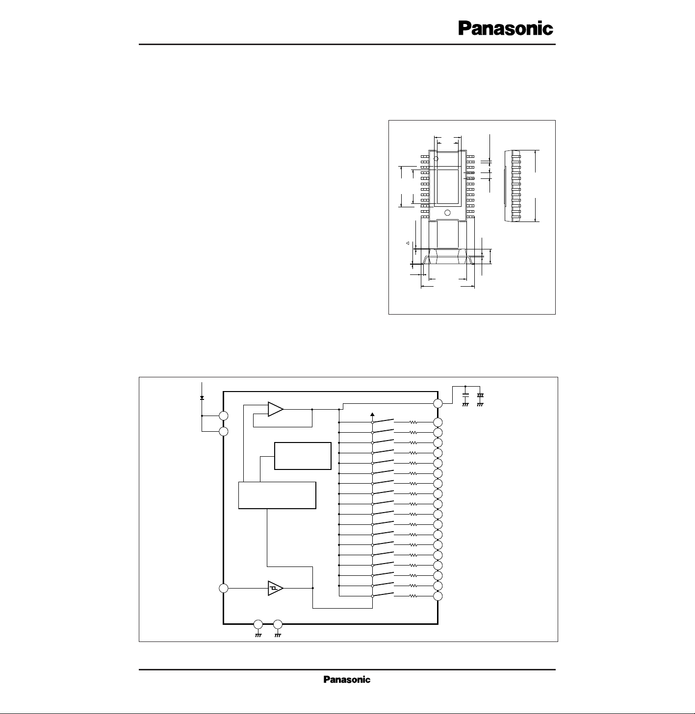
AN8612NSR
SCSI Active Terminator IC
8.4±0.3
11.73±0.3
0.5
0.1±0.1
(0075)
3.15±0.2
1.45
(7.8)
(9.2)
1.27 0.4±0.25
(6.0)
(4.6)
16.0±0.3
Unit : mm
1.45
1
2
4
5
6
7
8
9
11
12
3
10
24
23
22
21
20
19
18
17
16
15
14
13
Number in ( ) is a reference value.
24-pin SOP Package (HSOP024-P-0450)
(0.2)
■ Block Diagram
0.1µF
+
1µF
V
CC
12
13
STANDBY
24
+
–
Band Gap
Reference
6 19
Thermal
Shut Down
1
18
SG LINE 1
17
SG LINE 2
16
SG LINE 3
15
SG LINE 4
14
SG LINE 5
11
SG LINE 6
10
SG LINE 7
9
SG LINE 8
8
SG LINE 9
7
SG LINE 10
5
SG LINE 11
4
SG LINE 12
3
SG LINE 13
2
SG LINE 14
23
SG LINE 15
22
SG LINE 16
21
SG LINE 17
20
SG LINE 18
Page 2
V
CC
I
CC
P
D
T
opr
T
stg
Supply voltage
Supply current
Power dissipation
Note)
Operating ambient temperature
Storage temperature
V
mA
mW
˚C
˚C
Parameter Symbol Rating Unit
– 0.3 to + 7.0
500
2250
–20 to + 60
–55 to + 150
■ Recommended Operation Range (Ta=25˚C)
V
CC
Operating supply voltage
Parameter Symbol Range
4.0V to 5.5V
Parameter Symbol Condition min typ max Unit
■ Electrical Characteristics (VCC=5.0V, Ta=25±2˚C)
Supply current 1 44
I
CC1
54 mA
STANDBY= “L”
All SGLINE=open
STANDBY terminal “L” input current
Supply current 2 458
I
CC2
530 mA
STANDBY= “L”
All SGLINE=0.2V
V
CC
=5.5V, VI=0V
Supply current 3 100I
CC3
I
STBYL
200
1
µASTANDBY=open
–150 –50
1.3 1.5
µA
VSG=0.2VI
SG
19.8 23.0 26.2 mA
STANDBY terminal “L” input current VCC=5.5V, VI=5.5V
ISG=5mA to 15mA
I
STBYH
µA
1.7
STANDBY terminal positive direction
Threshold voltage
V
TH+
V
1.1 1.3 1.5
STANDBY terminal negative direction
Threshold voltage
V
TH–
V
Maximum output current SGLINE1-18
VCC=5.5V
STANDBY=open, V
SG
=0V
I
LK1
–1 µA
Output leak current 1
SGLINE1 to 18
VCC=5.5V
STANDBY=open, V
SG
=2.85V
I
LK2
–1 1 µA
Output leak current 2
SGLINE1 to 18
VCC=4.0 to 5.5V
All SGLINE=open
V
SGH
2.78 2.85 2.92 V
“H” level output voltage
SGLINE1 to 18
R
SG
107 115 123 Ω
Termination resistance value
SGLINE1 to 18
VCC=4.0 to 5.5V
All SGLINE=open
V
REG1
2.79 2.85 2.91 V
REG · output voltage
VCC=3.2V
All SGLINE=open
V
REG2
2.00 V
REG · output voltage
STANDBY terminal hysteresis width
V
HYS
mV
Output terminal capacitance
C
SG
8 pF
Thermal shut-down temperature T
TSD
˚C
(4.5)
(200)
(170)
Note) Number in ( ) is a design reference value but not guaranteed one.
Page 3

■ Package Power Dissipation
0 25 50 75 100 125 150
0
400
800
1200
1600
2000
2400
2800
3200
PD –Ta
Ambient Temperature Ta (˚C)
Evaluation PCB
(80.0 × 80.0 × 1.2mm)
T
jmax
=150˚C
P
D
=3100mW (25˚C)
Power Dissipation P
D
(mW)
Pin No.
Pin name
1
2
3
4
5
6
7
8
9
10
11
12
REGOUT
SGLINE14
SGLINE13
SGLINE12
SGLINE11
GND
Note 1)
SGLINE10
SGLINE9
SGLINE8
SGLINE7
SGLINE6
V
CC
(TERMPWR)
Note 2)
13
14
15
16
17
18
19
20
21
22
23
24
V
CC
(TERMPWR)
Note 2)
SGLINE5
SGLINE4
SGLINE3
SGLINE2
SGLINE1
GND
Note 4)
SGLINE18
SGLINE17
SGLINE16
SGLINE15
STANDBY
Note 3)
Pin No.
Pin name
terminal (One layer one surface GND of multi-layer board is recommended
for PCB.)
CC
should be connected with SCSI termination resistive power supply
TERMPWR.
<
VTH– for active mode and VI >VTH+
for stand-by mode Opening the STANDBY terminal also brings the stand-by
mode.
Page 4

■ Pin Descriptions
Equivalent circuit
Pin name
Pin No.
24 STANDBY
2, 3
4, 5
7, 8
9, 10
11, 14
15, 16
17, 18
20, 21
22, 23
SGLINE 1
12, 13 V
CC
1 REGOUT
SGLINE 18
—
24
2
V
CC
GND
V
CC
REGOUT
STANDBY
GND
115Ω
100kΩ
12
13
GND
1
V
CC
STANDBY
GND
20
kΩ
Page 5

The Interface Terminal Input Capacitance MAX25pF Stand-
ard are added from the SCSI II. This is because large stamp
input capacitance may prevent the normal signal transmission.
The capacitance value which does not cause the transmission
error differs, depending on the connection conditions of SCSI
equipment (such as distance between equipment, number of
equipment units and cable impedance), so, its proper value for
the AN8612NSR can not be identified. However, when the
input capacitance value specified in SCSII Standard,
MAX25pF is used, transmission error due to input capacitance
can hardly occur.
The input capacitance value is determined by the sum of the
following capacitances : active terminator (ex. 4.5 pF), printed
board (ex. 10 pF), driver receiver incorporated SCSI controller
(ex. 10 pF) and connector (ex. 0.5 pF).
Therefore, particular care should be taken to each device for
input capacitance.
For example, on the evaluation printed board of the
AN8612NSR, the measured capacitance value per signal line
is approx. 2.2 pF and that per unit area is 0.13 pF/mm2.
The thickness of printed board is 1 mm and the dielectric
constant of glass epoxy is 3.8 to 5.
For printed board, since the capacitance value differs,
depending on the thickness between layers and wiring length,
it should be measured actually. Also, it should be measured by
using the capacitance meter which can measure the capacitance value of semiconductor.
■ Precautions on Input Capacitance
Front Back
[
Evaluation Printed Board]
V
CC
STANBAY
GND
REGOUT
SGLINE18SGLINE1
AN8612NSR
V
CC
STANBAY
GND
REGOUT
SGLINE18SGLINE1
AN8612NSR
V
CC
STANBAY
GND
REGOUT
SGLINE18SGLINE1
AN8612NSR
SCSI equipment (CD-ROM)SCSI equipment (PC interface board) SCSI equipment (MO)
■ Application Circuit
 Loading...