

Page 1
ICs for Motor
AN8481SB
Spindle motor driver IC for optical disk
■ Overview
The AN8481SB is a high performance IC suited
for driving a spindle motor of an optical disk such
as CD-ROM, PD, DVD, CD-R, CD-RW, etc.
■ Features
• Adopting the 3-phase full-wave soft switch sys-
tem
• With switching regulator control function
• With start and stop pin
• Reverse breaking by EC/ECR voltage
• With Hall bias pin
• Surface-mount small package
■ Applications
• High speed CD-ROM drive
• PD, DVD, CD-R, CD-RW drives
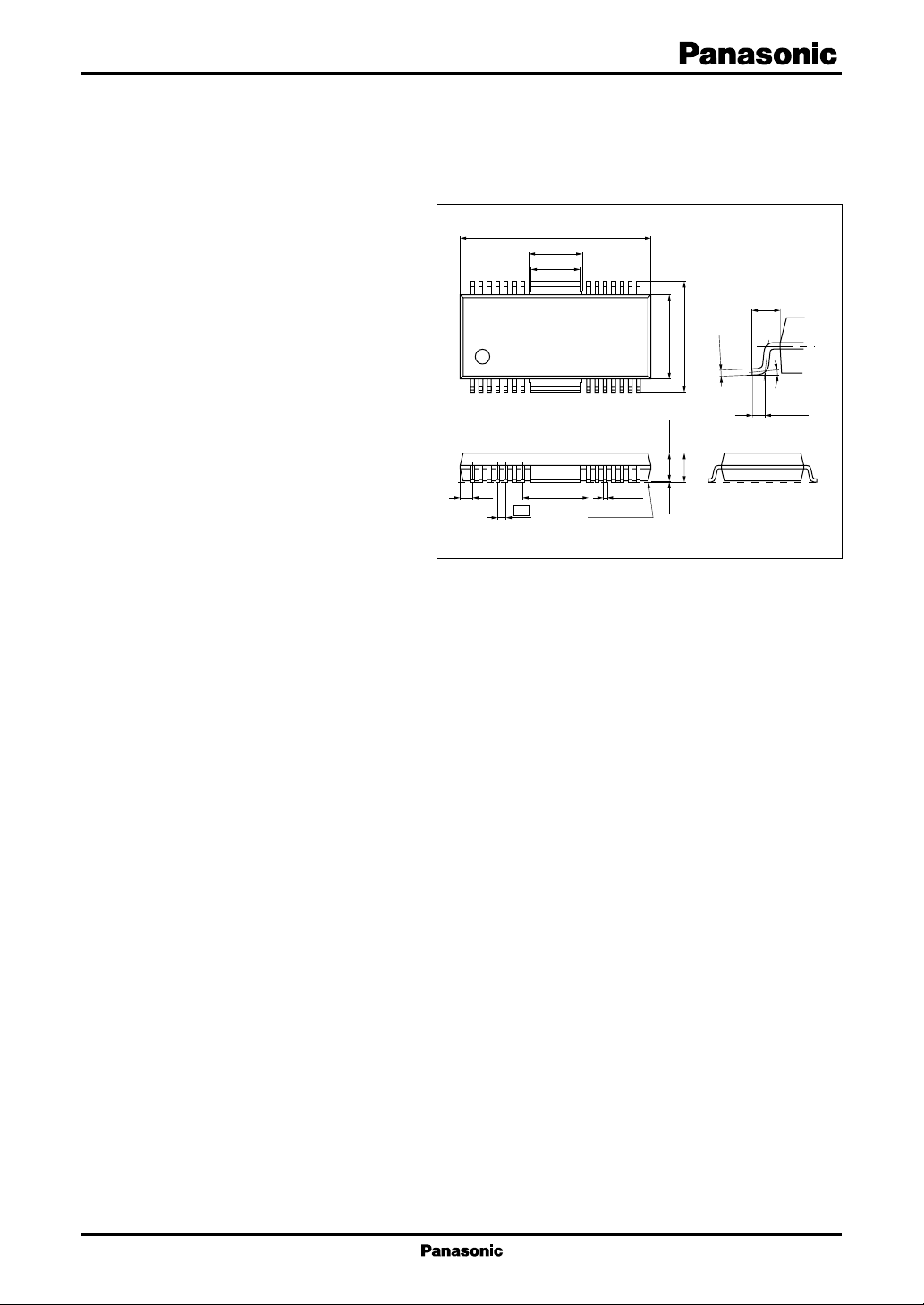
18.4±0.2
(5.15)
28 22 21
17 814
(1.2)
(4.8)
(6.4)
0.8
+0.10
0.35
–0.05
Seating plane
15
8.3±0.22.7±0.20.1±0.1
HSOP042-P-0400
+0.10
10.93±0.30
Unit: mm
(1.315)
–0.05
0.30
0° to 10°
0.65±0.20
1
Page 2
AN8481SB ICs for Motor
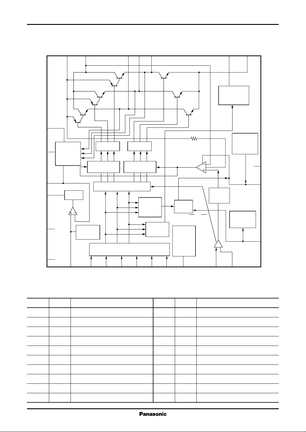
■ Block Diagram
REF
V
REG
PCS
SWB
SWG
GND
21
19
18
17
16
14
VM
20
Lower
side
V
CE
detection
Amp.
15
FC
CS1
22
Upper side
distribution
Triangular
wave
1
H1+
A1
27
26
Amp.
Amp.
Lower side
distribution
Direction changeover
Direction
detection
Hall amp. matrix
2
3
4
H1−
H2+
H2−
A2
25
Detection
5
A3
H3+
Logic
ER
EP = ER × EA
6
H3−
Hall
bias
7
VH
VTL
Absolute
value
EA
11
FG
9
FG
comparator
Start/stop
10
EC
PG
28
Thermal
protection
circuit
ECR
13
12
V
CC
PCI
8
S/S
■ Pin Descriptions
Pin No. Symbol Description
1H1+ Hall element-1 positive input pin
2H1− Hall element-1 negative input pin
3H2+ Hall element-2 positive input pin
4H2− Hall element-2 negative input pin
5H3+ Hall element-3 positive input pin
6H3− Hall element-3 negative input pin
7 VH Hall bias pin
8 SS Start/stop changeover pin
9 FG FG signal output pin
10 ECR Torque command reference input pin
2
Pin No. Symbol Description
11 EC Torque command input pin
12 PCI
13 V
Current feedback phase compensation pin
Supply voltage pin
CC
14 SG Signal GND pin
15 FC Triangular wave oscillation pin
16 SWG SW-REG system GND pin
17 SWB SW-REG driving pin
18 PCS
19 V
SW-REG system phase compensation pin
Fixed power supply pin
REG
20 VM Motor supply voltage pin
Page 3

ICs for Motor AN8481SB
■ Pin Descriptions (continued)
Pin No. Symbol Description
21 REF SW-REG reference setting pin
22 CS1 Current det. pin 1
23 N.C. N.C.
24 N.C. N.C.
■ Absolute Maximum Ratings
Parameter Symbol Rating Unit
Supply voltage V
4
Control signal input voltage
*
Supply current I
3
Output current
*
Hall bias current I
2
Power dissipation
Operating ambient temperature
Storage temperature
Note) Do not apply external currents or voltages to any pins not specifically mentioned.
For circuit currents, '+' denotes current flowing into the IC, and '−' denotes current flowing out of the IC.
1: Except for the operating ambient temperature and storage temperature, all ratings are for Ta = 25°C.
*
2: For 70°C and IC alone.
*
3: n = 22, 25, 26, 27, 28
*
4: n = 1, 2, 3, 4, 5, 6, 8, 10, 11
*
*
1
*
1
*
CC
V
M
V
REG
V
(n)
CC
I
O(n)
HB
P
D
T
opr
T
stg
Pin No. Symbol Description
25 A3 Drive output 3
26 A2 Drive output 2
27 A1 Drive output 1
28 PG Power GND pin
7.0 V
14.4
0 to V
CC
30 mA
±1 200 mA
50 mA
667 mW
−20 to +70 °C
−55 to +150 °C
V
■ Recommended Operating Range
Parameter Symbol Range Unit
Supply voltage V
CC
V
M
V
REG
■ Electrical Characteristics at Ta = 25°C
Parameter Symbol Conditions Min Typ Max Unit
Overall
Circuit current 1 I
Circuit current 2 I
Start/stop
Start voltage V
Stop voltage V
CC1
CC2
START
STOP
4.25 to 5.5 V
4.5 to 14
VCC = 5 V in power save mode 00.1mA
VCC = 5 V, IO = 0 mA 816mA
Voltage with which a circuit operates 3.5 V
at VCC = 5 V and L → H
Voltage with which a circuit becomes 1.0 V
off at VCC = 5 V and H → L
3
Page 4

AN8481SB ICs for Motor
■ Electrical Characteristics at Ta = 25°C (continued)
Parameter Symbol Conditions Min Typ Max Unit
Hall bias
Hall bias voltage V
Hall amplifier
Input bias current I
In-phase input voltage range V
Minimum input level V
Torque command
In-phase input voltage range EC VCC = 5 V 1 3.9 V
Offset voltage EC
Dead zone EC
Input current EC
Input/output gain A
Output
High-level output saturation voltage V
Low-level output saturation voltage V
Torque limit current I
FG
FG output high-level FG
FG output low-level FG
In-phase input voltage range V
FG hysteresis width H
Triangular wave oscillation circuit
Charging current I
Discharging current I
Lower side voltage detection circuit
Input to output gain G
SW-REG driving circuit
PNP driving current I
VCC = 5 V, IHB = 20 mA 0.7 1.2 1.6 V
HB
VCC = 5 V 15µA
BH
VCC = 5 V 1.5 4.0 V
HBR
VCC = 5 V 60 mV[p-p]
INH
VCC = 5 V −150 0 150 mV
OF
VCC = 5 V 50 100 150 mV
DZ
VCC = 5 V, EC = ECR = 2.5 V −5 −1 µA
IN
VDD = 5 V, RCS = 0.5 Ω 0.31 0.41 0.51 A/V
CS
VCC = 5 V, IO = −300 mA 0.9 1.6 V
OH
VCC = 5 V, IO = 300 mA 0.2 0.6 V
OL
VCC = 5 V, RCS = 0.5 Ω 390 530 670 mA
TL
VCC = 5 V, IFG = − 0.01 mA 3.0 V
H
VCC = 5 V, IFG = 0.01 mA 0.5 V
L
VCC = 5 V, 1.5 3.0 V
FGR
Input D-range at H2+, H2−
VCC = 5 V 1 10 20 mV
FG
VCC = 5 V, FC = 0.5 V −100 −50 −25 µA
CH
VCC = 5 V, FC = 2.5 V 25 50 100 µA
DCH
VCC = 5 V 5 10 20 times
V1
VCC = 5 V 10 50 mA
SWB
CC
V
• Design reference data
Note) The characteristics listed below are theoretical values based on the IC design and are not guaranteed.
Parameter Symbol Conditions Min Typ Max Unit
Thermal protection
Thermal protection operating T
SDONVCC
= 5 V, ∆EC = 100 mV 170 °C
temperature
Thermal protection hysteresis width ∆T
VCC = 5 V, ∆EC = 100 mV 45 °C
SD
4
Page 5

ICs for Motor AN8481SB
■ Usage Notes
Prevent this IC from being line-to-ground fault. (To be concrete, do not short-circuit any of pins A1 (pin 27), A2 (pin
26) and A3 (pin 25) to V
■ Application Notes
• PD Ta curves of HSOP042-P-0400
pin (pin 19) or VM pin (pin 20).)
REG
2 400
2 232
2 200
2 000
1 800
(mW)
D
1 600
1 400
1 200
1 042
1 000
Power dissipation P
800
Independent IC
without a heat sink
600
R
= 120°C/W
th( j-a)
PD = 1 042 mW (25°C)
400
200
0
0 25 150
50 75 100 125
Ambient temperature Ta (°C)
T
P
D
a
Mounted on standard board
(glass epoxy: 75 × 75 × t1.6 mm
R
= 56°C/W
th(j-a)
PD = 2 232 mW (25°C)
3
)
• Phase conditions between Hall input and output current
Phase of Hall pin
H1
H3
H1+ H3+H2+
A
HML
B
HML
C
MLH
D
LMH
E
LMH
F
MLH
A3 A3A2 A1 A2 A1
Emit
Output current
Sink
ABCDE
H2
H2H1
H3
0
ECR
EC
0
0
F
5
Page 6

AN8481SB ICs for Motor
■ Application Circuit Example
0.1 µF
= 0.5 Ω
R
CS
VM
20
CS1
22
A1
27
A2
26
A3
25
FG
9
PG
28
12 V
100 µF
68 µH
PCS
1 kΩ
REF
V
REG
1 µF
SWB
200 Ω
SWG
GND
21
19
18
17
16
14
Lower
side
V
CE
detection
Amp.
15
2 700 pF
FC
Upper side
distribution
Triangular
wave
1
H1+
Amp.
Direction changeover
Hall amp. matrix
2
H1−
Lower side
distribution
3
H2+
Amp.
4
H2−
Direction
detection
Detection
5
H3+
Logic
ER
EP = ER × EA
6
H3−
Hall
bias
7
VH
VTL
Absolute
value
EA
11
EC
FG
comparator
Thermal
protection
circuit
Start/stop
10
ECR
13
12
8
0.1 µF
S/S
VCC = 5V
V
CC
PCI
System
control
High: Start
command
Servo-torque
6
 Loading...