

Page 1
■ Overview
The AN8353UB is a dimmer IC to control illumination of the
car dashboard at high efficiency and high performance by pulse
width control. It outputs pulses at a duty proprotional to an
input voltage.
■ Features
•
Low power consumption by pulse control
•
External ON/OFF control by the standby pin
•
Pulse frequency range : 50Hz to 10kHz
•
Built-in overvoltage protective circuit approx. 20V
•
Wide operating ambient temperature range : –40˚C to+100˚C
•
All products temperature cycle, high reliability by normal
and high temperature checks reliability equivalent to the air
bags requested in U.S.
AN8353UB
High Efficiency Car Dashboard Dimmer IC
9
8
7
6
5
4
3
2
0.3
+0.1
– 0.05
23.3±0.3
6.0±0.3
2.4±0.25
3.3±0.25
1.5±0.25
0.5±0.1
2.54
1.5±0.25
1.4±0.3
30˚
3.0±0.3
Unit : mm
1
9-pin SIL Plastic Package (SIP009-P-0000C)
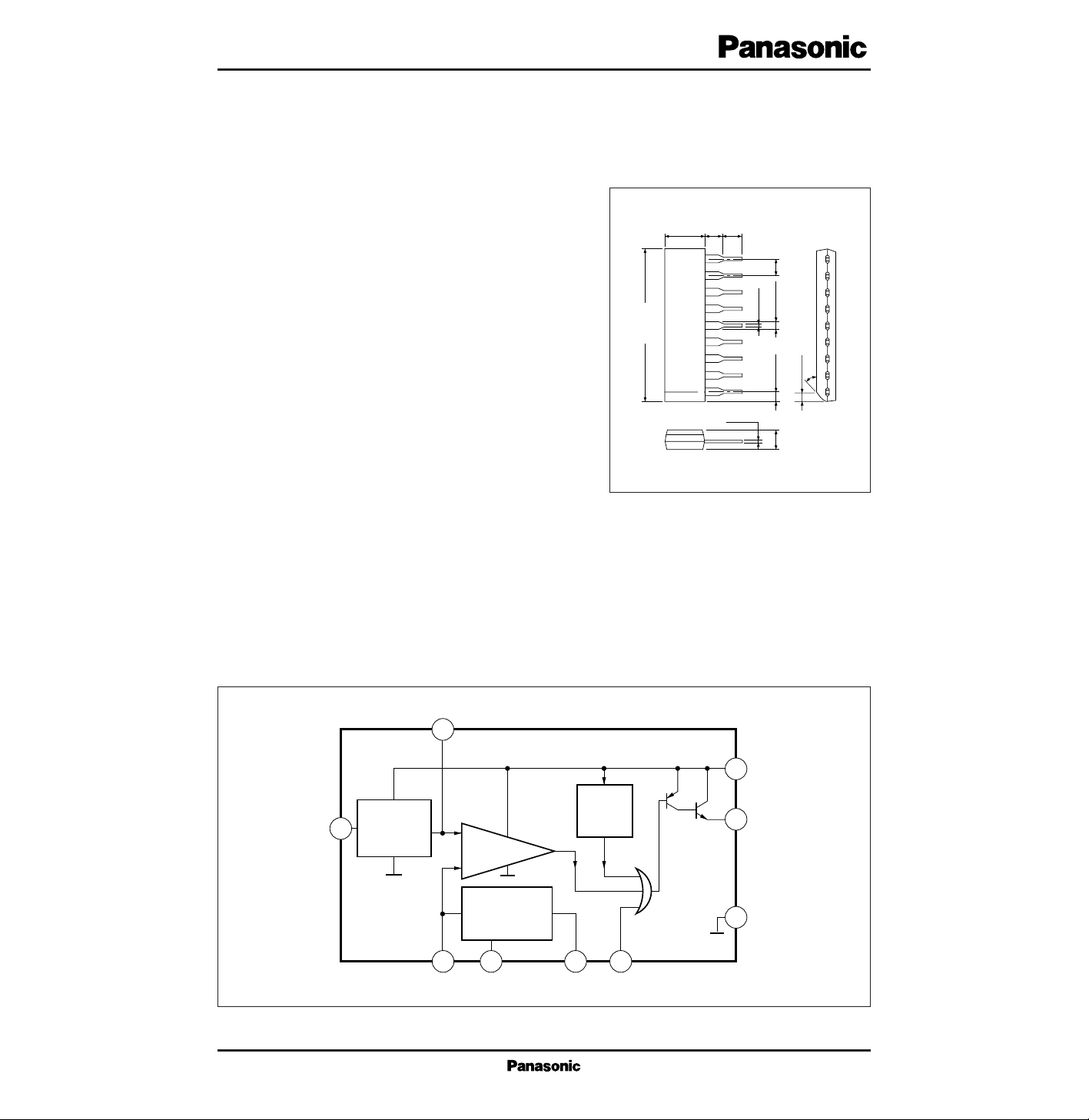
■ Block Diagram
3
Control
Voltage
Conversion
4
Over
Voltage
Protector
PWM
Comparator
Triangular
Wave Gen.
6 5 7 8
9
V
CC
1
GND
2
Page 2

Pin No.
Pin name
■ Pin Descriptions
Description
1 Output pin
Outputs an intermittent source current at a duty proportional to an input voltage
2 GND GND
3 Input pin Applies a control voltage.
4
Noise eliminating capacity connection pin 1
Connect a capacitor to eliminator a noise.
7
Noise eliminating capacity connection pin 2
Connect a capacitor to eliminator a noise.
9 V
CC
Supply Voltage
5 Square wave output pin
6 Triangular wave output pin
8 Standby pin
Output a triangular wave, which serves as a reference for the PWM signal,
to the Pin6 by connecting the resistor R
T
between the Pins5 and6, and
capacity C
T
between the Pin6 and GND.
Output a triangular wave, which serves as a reference for the PWM signal,
to this pin by connecting the resistor R
T
between the Pins6 and 5, and
capasity C
T
between the Pin6 and GND.
Forces to shut off an output current if a voltage higher than a threshold
voltage of 1.1V is applied to the Pin8.
V
CC
P
D
T
opr
T
stg
Supply voltage
Power dissipation
Storage temperature
Operating ambient temperature
V
mW
˚C
˚C
Parameter Symbol Rating Unit
■ Absolute Maximum Ratings (Ta=25˚C)
22
550
–40 to +100
–50 to +150
Parameter Symbol Range
■ Recommended Operating Range (Ta=25˚C)
Operating supply voltage range
V
CC
8 to 18V
Parameter Symbol Condition min typ max
■ Electrical Characteristics (Ta=25˚C)
Supply current
I
CC
11 mA7.5
Eliminate C
T
and R
T
Oscillation frequency
f
osc
Hz115
C
T
=0.027µF
0% duty input voltage
V
IN – 0
3 V2.5
C
T
=0.027µF
100% duty input voltage
V
IN– 100
V
C
T
=0.027µF
Center duty (VCC=12V)
D
12V
%45
C
T
=0.027µF
%
C
T
=0.027µF
Center duty (VCC=8V)
DD
8V
%0
C
T
=0.027µF
10
Center duty (VCC=18V)
DD
18V
%50
C
T
=0.027µF
Output duty gain
D
G
V
Output voltage at ON
V
ON
µA0
C
T
=2100pF
Leakage current at OFF
I
L
V20
C
T
=2100pF
22
1.65
4
55
1.2
10.5
140
55
1
1
18
45
0.6
4
90
2
9.5
35
–1
–1
Over voltage detection voltage
V
OV
CT=2100pF
V1.1
CT=2100pF
Standby threshold voltage
V
STH
0
0.9
0.55
Unit
Page 3

AN8353UB
+
±
AN8353UB
+
±
1
180Ω (3W)
10kΩ
10kΩ
2kΩ
C
T
R
T
20kΩ
180kΩ VR
20kΩ
180kΩ VR
0.056µF
0.056µF
0.1µF 0.1µF
C
T
R
T
0.1µF 0.1µF
33µF
22V
33µF
22V
2 3 4 5 6 7 98 1 2 3 4 5 6 7 98
1/f
OSC
=1.705RTC
T
1/f
OSC
=1.705RTC
T
• Bipolar Transister Output • MOS FET Output
■ Application Circuit
■ Supplementary Description
• System Operational Principle
The following describes the operational principle of the
system using the AN8353UB.
As shown in the block diagram in Fig. 1, a battery voltage
is divided by the VR and input to the input Pin3 in accordance with rotation amount. The voltage at the output Pin1 is
controlled by the AN8353UB so that the duty of the ON/OFF
period of the external output transistor will be proportional to
the input voltage, thus controlling a current flowing to the
lamps of the dashboard, etc. to adjust their brightness. Since
the output transistors are saturated at ON time and no current
flows at OFF time, power consumption is low.
The PWM method is used to control the output transistors.
This method, as shown in Fig. 2 I/O Characteristic Chart
(III), generates the triangular wave V6 as a reference signal
to generate pulses and input them to one end (Pin6) of the
PWM comparator. The triangular wave frequency f
OSC
can be
freely set from 50Hz to 10kHz, depending on the resistance
value RT connected between the square wave output Pin5 and
triangular wave output Pin6, and capacity value CT connected
between the triangular wave output Pin6 and ground Pin2.
The approximating expression for the then PWM frequency
f
OSC
is ;
1/f
OSC
=1.705CTRT ······················································(1)
For your refence, Fig. 3 shows the relations among CT, RT,
and oscillation frequency f
OSC
. The voltage V4, whose voltage
level is made matching the amplitude of the triangular wave
by the control voltage converter, is given to the other input
(Pin4) of the PWM comparator. That is, in Fig. 2 (II), the
input voltage V3 is linearly converted into V4 by the control
voltage converter so that the amplitude of the triangular wave
will be about 20% to 80% of the input voltage input range
(axis of abscissas in Fig. 2 (II)).
Then, a current is supplied from the output Pin1 to turn on
the output transistors during the period (TON) when the
inverted input voltage is larger than the triangular wave. (Fig.
2 (II), (IV)) To the contrary, while the converted input
voltage is smaller than the triangular wave, no current is
supplied from the output Pin1 and the output transistors are
turned off. The output pulse duty is expressed as follows.
Duty=T
ON
· f
OSC
······················································(2)
For the duty control characteristic of the output pulses to the
input voltage V3, the duty of the output pulses is controlled
from 0% to 100% at high-precision linearity while the “input
voltage V3/supply voltage V9” is between about
9
±
1
2
4
3
6 5 7 8
Control
voltage
converting
circuit
Over
voltage
protection
PWM
comparator
Tranguian
waveform
generator
–
+
0.1µF
C
1
R
T
C
T
0.1µF
STB
C
2
33µF
2kΩ
10kΩ
Battery
Fig. 1 AN8353UB Block Diagram
Page 4

0.2 (B-point) and 0.8 (C-point). The A-point in the figure
shows the I/O characteristics when the “input voltage V3/supply voltage V9” is 0.7. And, when V3/V9 is from 0.05V to
about 0.2V (B-point), the duty is controlled to 0%, and when
V3/V9 is from 0.8V (C-point) to t.0V, the duty is controlled to
100%.
The standby Pin8 can forcibly turn off the output transistors
by applying a voltage of about 1.1V or more to this pin.
When it is not necessary to forcibly turn off the output transistors, Leave the standby Pin8 open.
• System Operational Principle (cont.)
• Over voltage Detecting Voltage vs. Output
■ Supplementary Description (cont.)
D
1
V
9–2
V
OV
50%
0%
• Standby Threshold Voltage vs. Output
• Duty D
1
vs. Input Voltage VIN
(V
CC
=12V)
D
1
V
8–2
V
STH
0
50%
D
1
V
IN
V3/V
9
V3/V
9
V4/V
9
V4/V
9
V6/V
9
max V6/V
9
V
1
1
t
T
ON
Duty=T
ON
· f
OSC
1/f
OSC
t
10.5
0.5 1
B
B´
A´
C´
100%
50%
0.5
0
0%
Duty
(I)
(III)
(IV)
(II)
Turn-up Line
Fig. 2 I/O Characteristic Chart
Fig. 3 Relations between Oscillation Frequency and CT and R
T
A
C
V
IN–0
V
IN–100
4V 6V 8V
100%
0%
D
12V
D
G
· Output voltage at ON V
ON
· Leakage current at OFF
V
ON=VCC –V1–2
IL=
V
1–2
IMΩ
0%
max V6/V
9
Resistance RT (Ω)
1M
Oscillation Frequency f
OSC
(Hz)
1k
100k
10k
1k
100
10
10k 100k 1M 10M
VCC=12V
V
IN
=6V
CT=0.001µF
CT=0.01µF
CT=0.1µF
CT=1µF
 Loading...