

Page 1
ICs for TV
■ Overview
The AN8146FBQ is a 10-bit D/A converter IC for TV
image processing. It is a Bi-CMOS IC featuring low power
consumption. It includes 3 channels of I/O. It is suitable
for high-definition TV and computer monitor.
■ Features
●
High-speed conversion : 50MSPS
●
Low power consumption : 450mW
●
3 channels of I/O
●
Input level : TTL level
●
Single power supply : 5V
●
Reference voltage source built-in
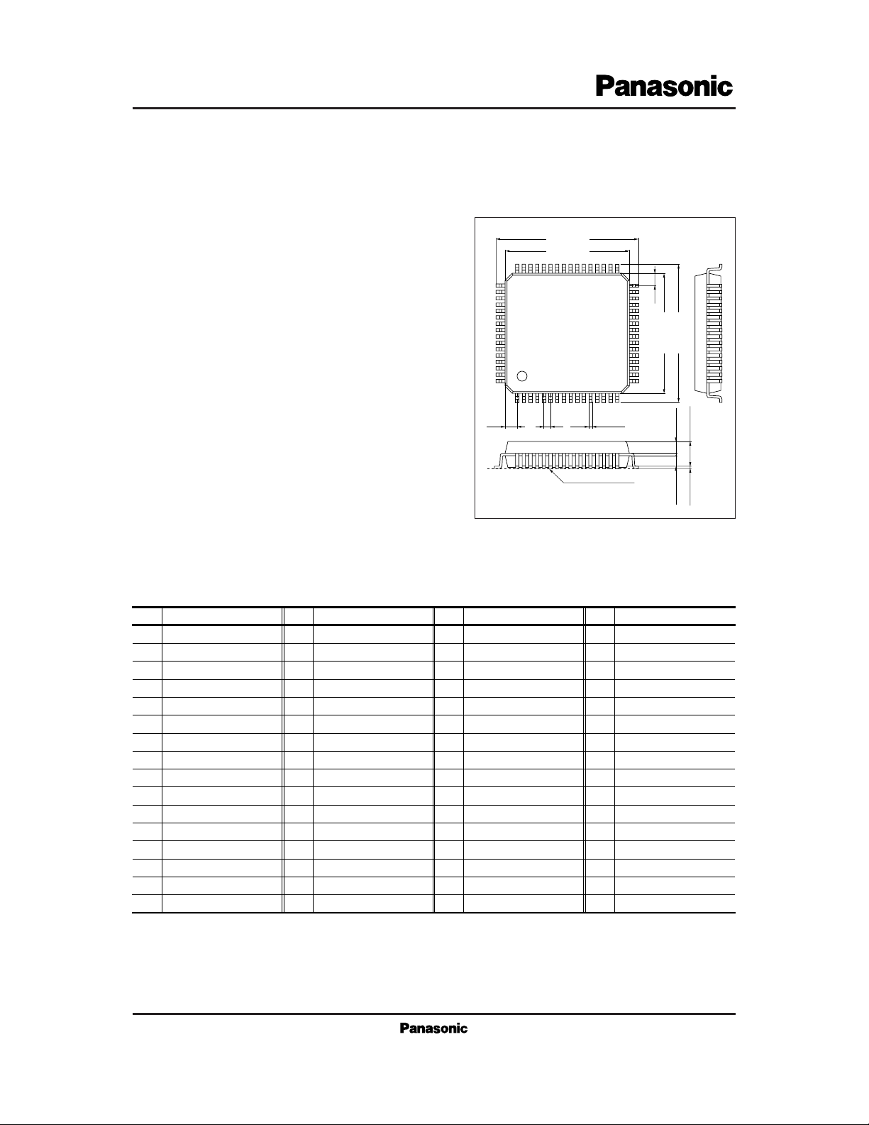
AN8146FBQ
10-Bit 3-channel D/A Converter IC
14.0±0.30
1
17
32
64
49
(10)
(10) 0.35
SEATING PLANE
14.0±0.30
17.2±0.40
0.1±0.1 1.95±0.2
0.9±0.10.9±0.1
+ 0.10
– 0.05
16
48 33
16.2±0.3
Unit : mm
64-Pin QFS Package (QFS064-P-1414B)
■ Pin Descriptions
Pin No.
1
2
3
4
5
6
7
8
9
10
11
12
13
14
15
16
Pin name
Analog GND
Digital input 1 bit (MSB)
Digital input 2 bit
Digital input 3 bit
Digital input 4 bit
Digital input 5 bit
Digital input 6 bit
Analog GND
Analog GND
Analog GND
Digital input 7 bit
Digital input 8 bit
Digital input 9 bit
Digital input 10 bit (LSB)
Clock input
Digital GND
A
A
A
A
A
A
A
A
A
A
A
Pin No.
17
18
19
20
21
22
23
24
25
26
27
28
29
30
31
32
Pin name
Digital input 1 bit (MSB)
Digital input 2 bit
Digital input 3 bit
Analog GND
Analog GND
Digital input 4 bit
Digital input 5 bit
Digital input 6 bit
Analog GND
Analog GND
Digital input 7 bit
Digital input 8 bit
Digital input 9 bit
Digital input 10 bit
Clock input
Digital power supply
B
B
B
B
B
B
B
B
B
B
B
Pin No.
33
34
35
36
37
38
39
40
41
42
43
44
45
46
47
48
Pin name
Analog GND
Digital input 1 bit (MSB)
Digital input 2 bit
Digital input 3 bit
Digital input 4 bit
Digital input 5 bit
Digital input 6 bit
Analog GND
Analog GND
Analog GND
Digital input 7 bit
Digital input 8 bit
Digital input 9 bit
Digital input 10 bit
Clock input
Analog GND
C
C
C
C
C
C
C
C
C
C
C
Pin No.
49
50
51
52
53
54
55
56
57
58
59
60
61
62
63
64
Pin name
Reference voltage output
Reference voltage input
Analog GND
Analog GND
To a compensation capacitor
Stabilizing
Reference resistance
Analog GND
Analog GND
Analog GND
Analog output C
Analog power supply
Analog output B
Analog power supply
Analog output B
Analog GND
Page 2
ICs for TV
AN8146FBQ
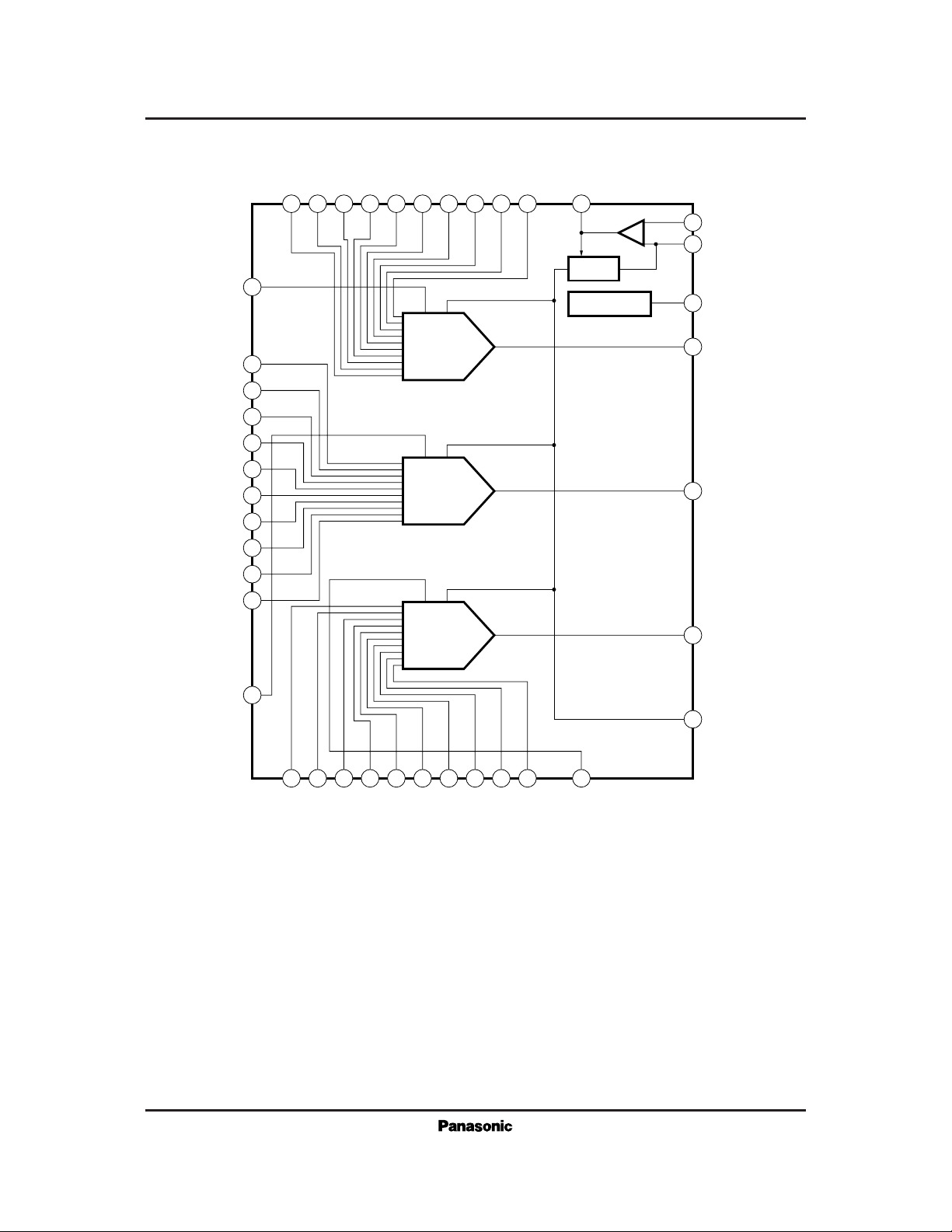
■ Block Diagram
14 213 12 11 7 6 5 4 3 53
34 4635 36 37 38 39 43 44 45 47
31
30
29
28
27
24
23
22
19
18
17
15
10-bit D/A A
50
55
49
63
61
59
10-bit D/A B
10-bit D/A C
Current
Source
Refference
Voltage Regulator
D10A D1AD9A D8A D7A D6A D5A D4A D3A D2A COMP
D1C D10CD2C D3C D4C D5C D6C D7C D8C D9C CLKC
CLKB
D10B
D9B
D8B
D7B
D6B
D5B
D4B
D3B
D2B
D1B
CLKA
REFI
REFR
REFO
OUTA
OUTB
OUTC
VIB
+
–
54
Page 3

ICs for TV
AN8146FBQ
Parameter Symbol Rating Unit
V
CC
I
CC
P
D
T
opr
T
stg
Supply voltage
Supply current
Operating ambient temperature
Note 1)
Power dissipation
Note 2)
Storage temperature
Note 1)
– 0.3 to + 7.0
210
585
– 20 to + 70
– 55 to + 125
V
mA
mW
˚C
˚C
Note 1) Ta =25˚C except operating ambient temperature and storage temperature.
Note 2) Allowable power dissipation of the package at Ta =70˚C.
■ Absolute Maximum Ratings
Parameter Symbol Range
Operating supply voltage range
V
CC
4.75V to 5.25V
■ Recommended Operating Range (Ta = 25˚C)
Parameter minCondition typ max UnitSymbol
I
CC
Supply current
150 mA
I
DI
V
IN
= 5V (HI), V
IN
= 0V (LO)
Digital input leak current
± 30 µA
I
REFI
V
IN
= 5V (HI), V
IN
= 0V (LO)
REF leak current
± 30 µA
90
V
REFO
I
REFO
= 3.0mA
Reference supply output voltage
3.24 V2.7
R
ES
Resolution
Bit10
E
L
Linearity error
±1.0 LSB± 0.5
E
D
Differential linearity error
LSB
V
FS
R
REF
= 350Ω
RO = 75Ω
V
REFO
– V
REFI
= 1.4V
Full scale output voltage
5.1 V5.0
V
ZS
Zero scale output voltage
4.2 V4.0
F
CMAX
Maximum conversion rate
MSPS
M
Z
V
ZS
= 4.0V
Zero scale matching
± 4%
2.06
±1.0± 0.5
50
3.8
4.9
■ Electrical Characteristics (AVCC= DVCC= 5.0V, Ta= 25±2˚C)
D
f
OUT
= 10MHz
2nd harmonics level
dB
CT
f
OUT
= 10MHz
Crosstalk
dB
(– 38)
(– 43)
Note) The characteristics value in parentheses is not a guaranteed value, but reference one on design.
Page 4

ICs for TV
AN8146FBQ
1.3 V
min typ max Unit
Ω
V
REFI
Reference voltage
Parameter ConditionsSymbol
R
O
Output load resistance
Note
2.4 DV
CC
V
V
IH
Digital input voltage
0 0.8 V
V
IL
Digital input voltage
t
WH
Clock pulse width
Refer to the timing chart. 1
t
WL
Clock pulse width
Refer to the timing chart. 1
t
S
Set-up time
Refer to the timing chart.
t
H
Holding time
Refer to the timing chart.
030
I
OUT
Analog output current
2mA
–10 0
I
REFO
Reference power supply output current
2mA
– 0.3 AV
CC
V
REF1
Reference voltage input voltage
2V
75
8ns
8ns
5ns
1ns
Note 1) t
WH
+ t
WL
≥20ns
Note 2) Use it under the condition : AV
CC
= DVCC, and AGND = DGND
(Cautions on surge)
Comparing with the other pins, Pin50 has a lower negative-surge resistance (Approx. –190V at 200pF).
Therefore, particular care must be taken when it is used.
■ Operation Descriptions
●
Recommended Operating Conditions (AV
CC= DVCC= 5.0V,
Ta= 25±5˚C)
●
Operational Timing
Clock input
Data input
Dn – 1
t
WH
Dn Dn + 1
t
WL
t
H
t
S
■ Reference
1,400
1416
1,200
1,000
800
861
600
400
200
0
0 25 50 75 100 150
Ambient Temperature Ta (˚C)
125
Power Dissipation P
D
(mW)
Power Dissipation on Package
PD – Ta
Glass epoxy board
(50
× 50 × 0.8tmm)
R
thj – a
= 70.6˚C/W
P
D
=1416mW (25˚C)
IC without heat sink
R
thj – a
=116.2˚C/W
P
D
= 861mW (25˚C)
 Loading...