

Page 1
1
A/D and D/A Converters
■ Overview
The AN8140K is a 10-bit D/A converter for image processing which has realized low power comsumption by
using the Bi-CMOS process.
■ Features
• 10-bit resolution
•
High speed : maximum conversion rate of 50MSPS
•
Low power comsumption : 150mW
•
TTL compatible input level
•
Single 5V power supply
•
Built-in reference power supply
■ Application Field
•
Image equipment such as hi-vision device
•
OA equipment such as image scanner
•
Measuring equipment such as digital oscilloscope
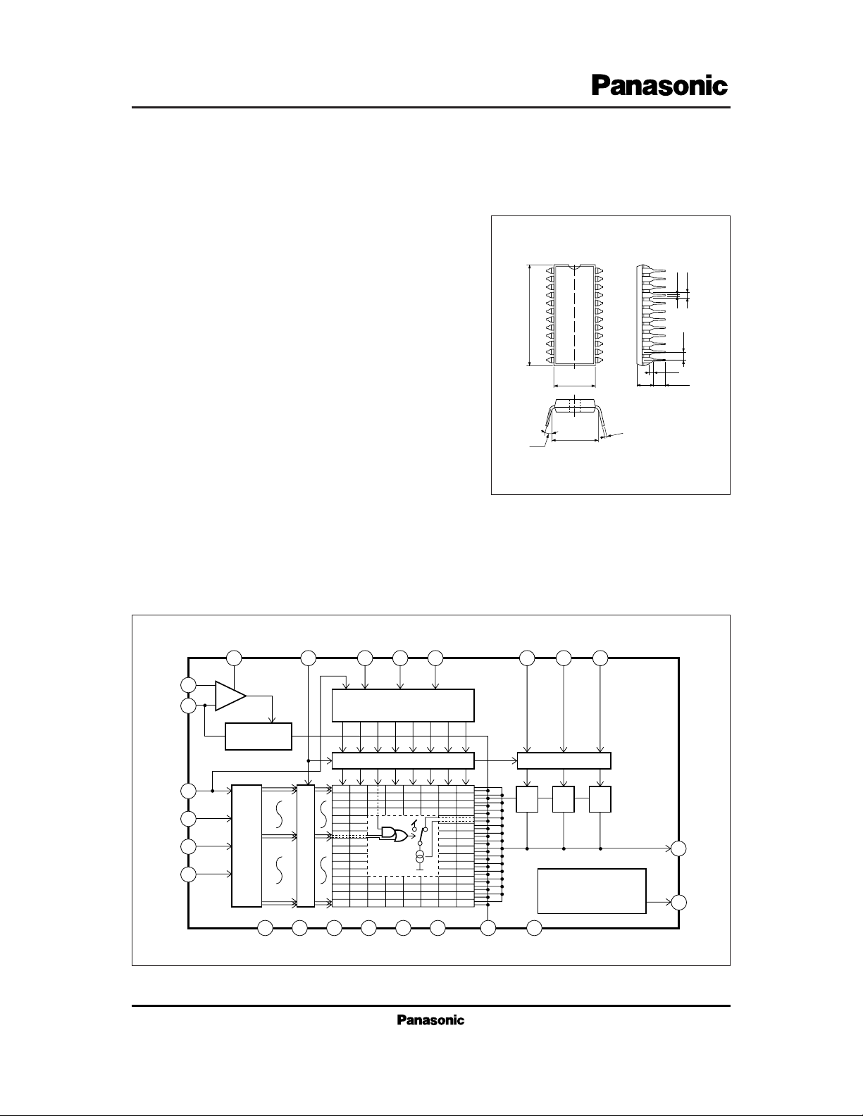
AN8140K
High-speed Low Power Consumption 10-bit D/A Converter
Unit : mm
24-pin Shrunk DIL Plastic Package (SDIP024-P-0300)
7.62±0.25
21.7±0.3
0.3±
+ 0.2
– 0.05
3 ∼15˚
6.2±0.3
0.5±0.1
0.9±0.25
1.778
4.7±0.25
3.05±0.25
1.1±0.25
1
2
3
4
5
6
7
8
9
10
11
12
24
23
22
21
20
19
18
17
16
15
14
13
■ Block Diagram
REFI
IREF
D6
D7
D8
D9
(MSB)
COMP CLK D5 D4 D3 D2 D1
9 14 19 20 21 22 23 24
+
7
10
18
17
16
15
–
Current
Source
X– Decoder
AGND DV
Latch
DGND AVCCAV
CC
X – Decoder
Latch
CC
AGND
VIB NC
1/2 1/4 1/8
8 13 13 2 11 12 4
(LSB)
D0
Latch
Reference
Voltage Regulator
OUT
5
6
REFO
Page 2
2
A/D and D/A Converters
AN8140K
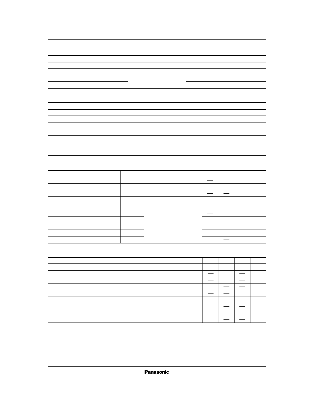
Parameter Condition Rating Unit
Resolution 10 bit
Linearity error R
REF
= 470Ω ±1.0 LSB
Differential linearity error R
O
= 75Ω ±1.0 LSB
Maximum conversion rate V
REFO –VREFI
= 1.4V 50 MSPS
■ Main Characteristics (VCC=5.0V, Ta=25˚C)
V
CC
V
IN
I
O
V
REFI
P
D
T
opr
T
stg
Supply voltage
Digital input voltage
Analogue output current
Reference input voltage
Power dissipation
Operating ambient temperature
Storage temperature
V
V
mA
V
mW
˚C
˚C
Paremeter Symbol Rating Unit
■ Absolute Maximum Rating (Ta=25˚C)
– 0.3 to +7.0
– 0.3 to DV
CC
30
– 0.3 to AV
CC
700
–20 to + 70
–55 to +150
VIN= 0V, 5V
VIN= 0V, 5V
I
REFO
= 3.0mA
Parameter Symbol Rating min typ max Unit
■ Electrical Characteristics (VCC=5.0V, Ta=25˚C)
I
CC
I
LK1
I
LK2
V
REFO
E
L
E
D
F
C
V
FS
V
ZS
t
ST
2.16
50
4.9
3.8
30
2.7
±0.5
±0.5
5.0
4.0
50
±30
±30
3.24
±1
±1
5.1
4.2
20
mA
µA
µA
V
LSB
LSB
MSPS
V
V
ns
Supply current
Digital input leak current
REFI input leak current
Reference output voltage
Linearty error
Differential linearty error
Maximum conversion rate
Full-scale output voltage
Zero-scale output voltage
Settling time
R
REF
= 470Ω
RO= 75Ω
V
REF0 –VREFI
= 1.4V
Parameter Symbol Conditions min typ max Unit
Supply voltage V
CC
4.75 5.0 5.25 V
Regerence voltage v
REFO
= 2.7V V
REFI
RO = 75Ω, R
REF
= 470Ω 1.3 V
Output load resistance R
O
75 Ω
Digital input voltage
V
IH
2.4 V
V
IL
0.8 V
Clock input pulse width
t
WH
*1 8 *2 ns
t
WL
*1 8 *2 ns
Setting-up time t
S
*1 5 ns
Holding time t
H
*1 1 ns
■ Recommended Operating Conditions (Ta=25˚C)
*1 : Refer to the timing chart.
*2 : tWH+tWL≥20ns
Page 3

3
A/D and D/A Converters
AN8140K
■ Pin Descriptions
Pin No.
Pin nameSymbol Symbol
1
2
3
4
5
6
7
8
9
10
11
12
No connection pin
Digital GND
Analogue GND
Analogue GND
Analogue output
Reference voltage output
Reference voltage input
Stabilized capacitive pin
Compensation capacitive pin
Reference current pin
Analogue power supply
Analogue power supply
NC
DGND
AGND
AGND
OUT
REFO
REFI
V
IB
COMP
I
REF
AV
CC
AV
CC
Digital power supply
Clock input
Digital input 1-bit (MSB)
Digital input 2-bit
Digital input 3-bit
Digital input 4-bit
Digital input 5-bit
Digital input 6-bit
Digital input 7-bit
Digital input 8-bit
Digital input 9-bit
Digital input 10-bit (LSB)
DV
CC
CLK
D9
D8
D7
D6
D5
D4
D3
D2
D1
D0
Pin No.
Pin name
13
14
15
16
17
18
19
20
21
22
23
24
CLK
Dn – 1
DATA
OUT
t
H
t
WH
An – 2
t
WL
t
S
Dn Dn+1
t
ST
An – 1 An
■ Timing Chart
Page 4

4
A/D and D/A Converters
AN8140K
■ Output Code
Step
Digital input
0123456789
0000000000
0000000001
·
·
·
0111111111
1000000000
1000000001
·
·
·
1111111110
1111111111
Output voltage
V
OUT
4.0000
4.0010
·
·
·
4.4995
4.5005
4.5015
·
·
·
4.9990
5.0000
000
001
·
·
·
511
512
513
·
·
·
1022
1023
■ Application Circuit
AVCCDVCCAGND DGND
+
+
75ΩR
o
10kΩ
5kΩ
RREF
1µF
470Ω
(MSB)
(LSB)
CLK
DIGITAL IN
NC
DGND
AGND
AGND
OUT
REFO
REFI
VIB
COMP
IREF
AV
CC
AV
CC
D0
D1
D2
D3
D4
D5
D6
D7
D8
D9
CLK
DV
CC
LOW PASS
FILTER
Video Signal
OUT
+
+
 Loading...