

Page 1
ICs for CD/CD-ROM Player
■ Overview
The AN8086S is an IC for controlling a DC-DC converter
suitable for the switching power supply of various
portable equipment. It can operate with input voltage
1.1V or more. The AN8086S is based on AN8083S with
the output voltage in the secondary side changed to 3.6V.
■ Features
•
Operatable with low voltage input (PV
CC
>1.1V)
•
Decreased voltage detection circuit built-in
•
Short-circuit protection feature built-in
•
Provided with reset output
•
Synchronizable with outside clock
•
Low consumption current in stand-by mode
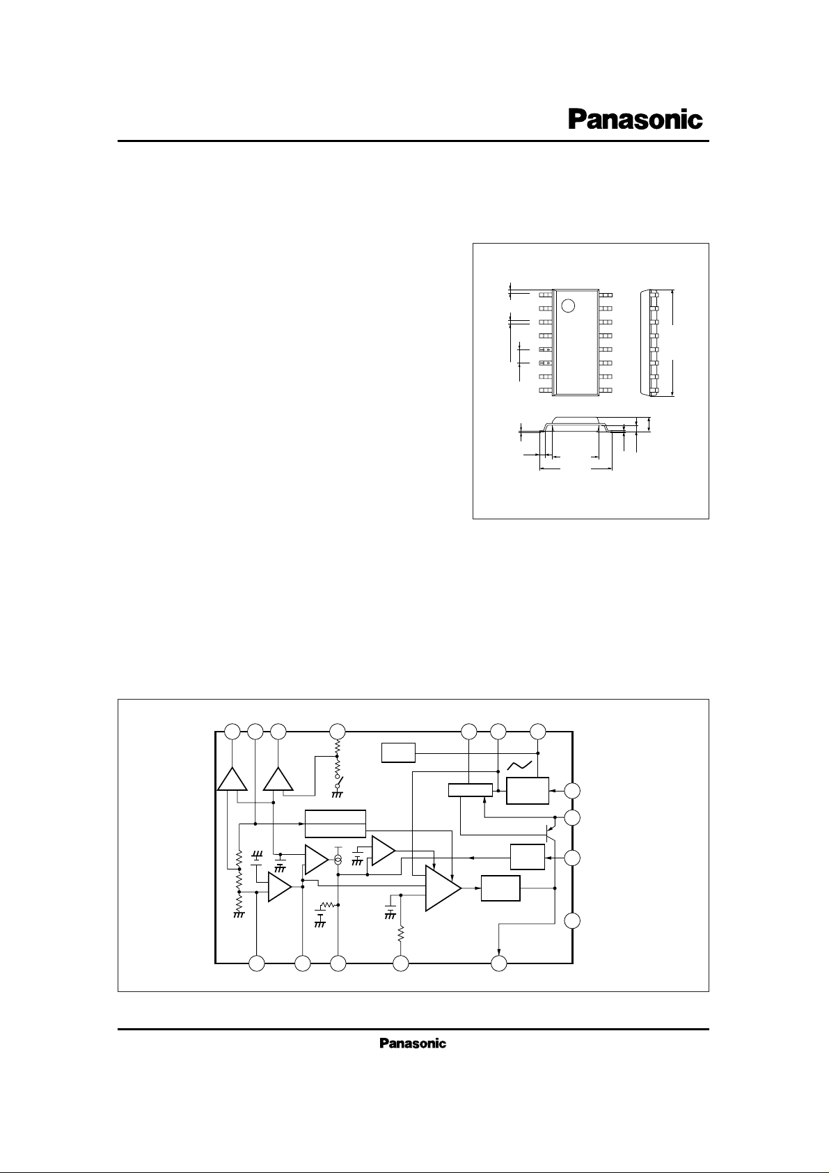
AN8086S
Low Voltage Operation IC for DC-DC Converter
0.1±0.1
1.5±0.2
0.3
0.65
0.15
0.4
1
2
3
4
5
6
7
8
16
15
14
13
12
11
10
9
0.4±0.25
1.27
Unit : mm
6.5
±0.3
4.2±0.3
10.1±0.3
16-lead SOP package (SOP016-P-0225A)
15 1316 14 7
1 2 3 4 5
6
V
CC
PV
CC
10 12
9
8
11
Power
Off
63kΩ
–+
GND
0.9V
1.25V
0.7V
3.24V
0.725V
30kΩ
2.0V
4.8V
2.7V→ 2.5V
2.2V
0.25V
0.85V
V
REF
–
+
–
+
–
+
RESET EMP V
SEN
IN FB SPRO DED OUT
START CT V
REF
POWER
CLK
Starter
Triangular
Wave
Switching
Circuit
Starter SW
Early Value Set.
–+
+
–
+
■ Block Diagram
Page 2
ICs for CD/CD-ROM Player
AN8086S
■ Absolute Maximum Ratings (Ta=25˚C)
V
CC
PV
CC
P
D
T
opr
T
stg
Supply Voltage
Power Dissipation
Operating Ambient Temperature
Storage Temperature
V
mW
˚C
˚C
Parameter Symbol Rating Unit
14.4
14.4
380
–20 ~ +75
–55 ~ +125
■ Recommended Operating Range (Ta=25˚C)
Parameter Symbol Range
Operating Supply Voltage Range
V
CC
PV
CC
3.6V ~ 12V
1.1V ~ 12V
■ Electrical Characteristics (Ta=25˚C)
Parameter Symbol Condition min. typ. max. Unit
Power VCC Stand-by Mode Supply Current
I
PVCC
2 µA
V
CC
=0V, PVCC=3V
Power VCC No Load Supply Current
I
PVCC
3 mA1.2
V
CC
=3.1V, PVCC=3V
Output Voltage
V
O
V3.6
Reset Output Threshold Voltage
V
TH (RESET)
V
Decreased Voltage Detection Threshold Voltage
2.1V
TH (VSEN)
2.3 V2.2
Short-Circuit Protection Operating Voltage
1.35V
O (SPRO)
2.1 V
V
IN
=0V, V
POWER
=2V
Short-Circuit Protection Operating Voltage
1.7V
O (SPRO)
3.2 V
V
IN
=1V, V
POWER
=0V
Triangular oscillation Frequency in Normal Operation
60f
OSC1
80 kHz70
R
REF
=33kΩ, CT=330pF
f
OSC2
80 100 120 kHzTriangular oscillation Frequency at Start
R
REF
=33kΩ, CT=330pF
V
CC
=1.9V, PVCC=3V
Output Voltage
1.2V
OH (OUT)
1.6 V
I
O
=–20mA, VCT=0V
Output Voltage
V
OL (OUT)
0.4 V
I
O
=20mA, VCT=1V
Note) Unless otherwise specified, V
CC
=4.8V, PVCC=3V
V
TH
× 0.85
V
TH
× 9V
TH
× 0.95
15 16 13 14 10 7 12
9
8
11
6
54321
+
2.2V
V
REF
4.8V
3.24V
0.7V
1.25V
2.0V
0.9V
30kΩ
–25µA
0.725V
63kΩ
+
–
+
–
+
–
+
–
+
+ –
2.7V→ 2.5V
33kΩ
0.01µF
IN FB
SPRO
47µF
DED
0.01µF
OUT
GND
0.01µF
100Ω
POWER
CLK
PV
CC
3.6V
33kΩ330pF
V
REF
CT
START
V
SENSE
EMP
V
CC
+–
Power
OFF
0.25V
0.85V
RESET
Starter
Triangular
Wave
Swiching
Circuit
Starter SW
Early Value Set.
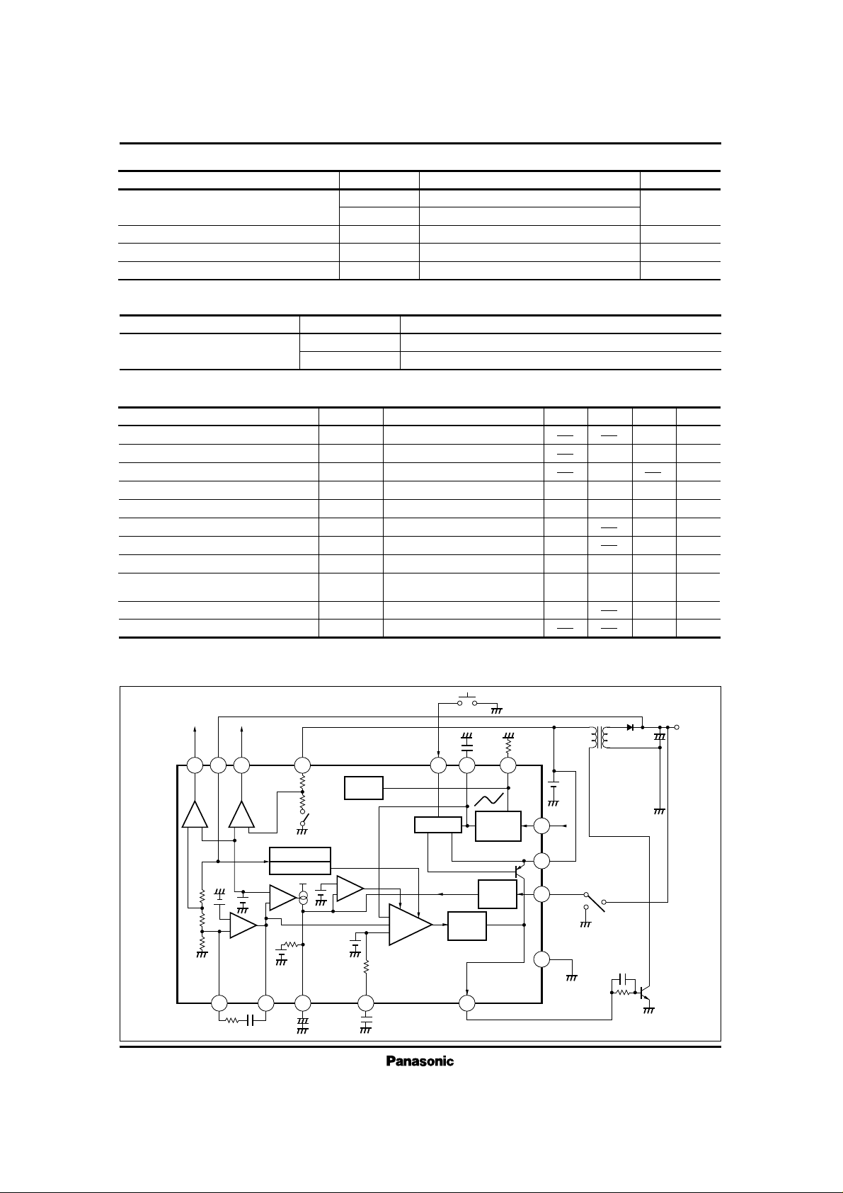
■ Application Circuit Example
Page 3

ICs for CD/CD-ROM Player
AN8086S
■ Pin Description
Pin No.
Symbol
1 IN
•
Input pin for error amplifier
• Threshold voltage ; 0.7V
2 FB • Output pin for error amplifier
•
Short-circuit protection input pin
If output of error amplifier does not become “L” when t = CVth/I
SPRO
output of IC is not
switched. I
SPRO
=25µA
V
th
= 0.9V
3 SPRO
4 DED
5 OUT
•
Switching output pin
Output current ; IO=20mA (max.)
6 GND • GND pin
• Triangular oscillating capacitor pin
7 CT
8 PV
CC
• DC voltage input pin
Operates with 1.1V or more.
•
Clock input
· It is used to synchronize triangular oscillation with clock input and operates at rise edge of
clock.
· The threshold level is TTL level.
· It is open when not used.
9 CLK
•
Start pin
· Starts switching of starter (start at “L”)
· Threshold voltage, PV
CC
– 0.9V
10 START
11 POWER
•
Power ON/OFF pin
Output ON/OFF switching pin (Output is off at “L.”)
T
1
T
2
V
T1 =
CV
I (Discharged)
f =
1
T
1
+ T
2
T2 =
CV
I (Charged)
I (Discharged) =52µA
I (Charged) =30µA
V = 0.58V
In normal operation
• Reference voltage pin
· 1.25V output
· Charged and discharged current of triangular oscillation is determined by external R.
I (Charged) =
V
REF
– 0.7
R
REF
+1kΩ
I (Discharged)=1.40 × I (Charged)
12 V
REF
13 EMP
•
Decreased voltage detection output pin
“H” when detected by open collector output form
14 V
SEN
• Decreased voltage detection input pin
· Threshold voltage ; 2.2V
•
Reset output pin
· “H” when VCC becomes VO × 0.9V or more
· Open collector output form
15 Reset
16 V
CC
• DC voltage input pin
Operates with 3.6V or more.
•
Dead time control input
Maximum duty ratio set to 85%.
Description
 Loading...