

Page 1
AN8000/AN8000M Series
3-pin Positive Output Low Dropout Voltage Regulator (50mA Type)
■ Overview
The AN8000 series is 3-pin low-dropout fixed positi ve
output monolithic voltage regulators. Since thier power
consumption can be minimized, they are suitable for battery stabilizing power supply and reference voltage. Thir teen types of output voltage are available ; 2V, 2.5V, 3V,
3.5V (TO-92 only) , 4V, 4.5V, 5V, 6V, 7V, 8V, 8.5V, 9V,
and 10V.
■ Features
• Input/output voltage difference : 0.3V (max.)
• Output current of up to 50mA
• Low bias current ; 0.6mA (typ.)
• Output voltage ; 2V, 2.5V, 3V, 3.5V (TO-92 only) , 4V ,
4.5V, 5V, 6V, 7V, 8V, 8.5V, 9V, and 10V.
• Over-voltage protective circuit built-in.
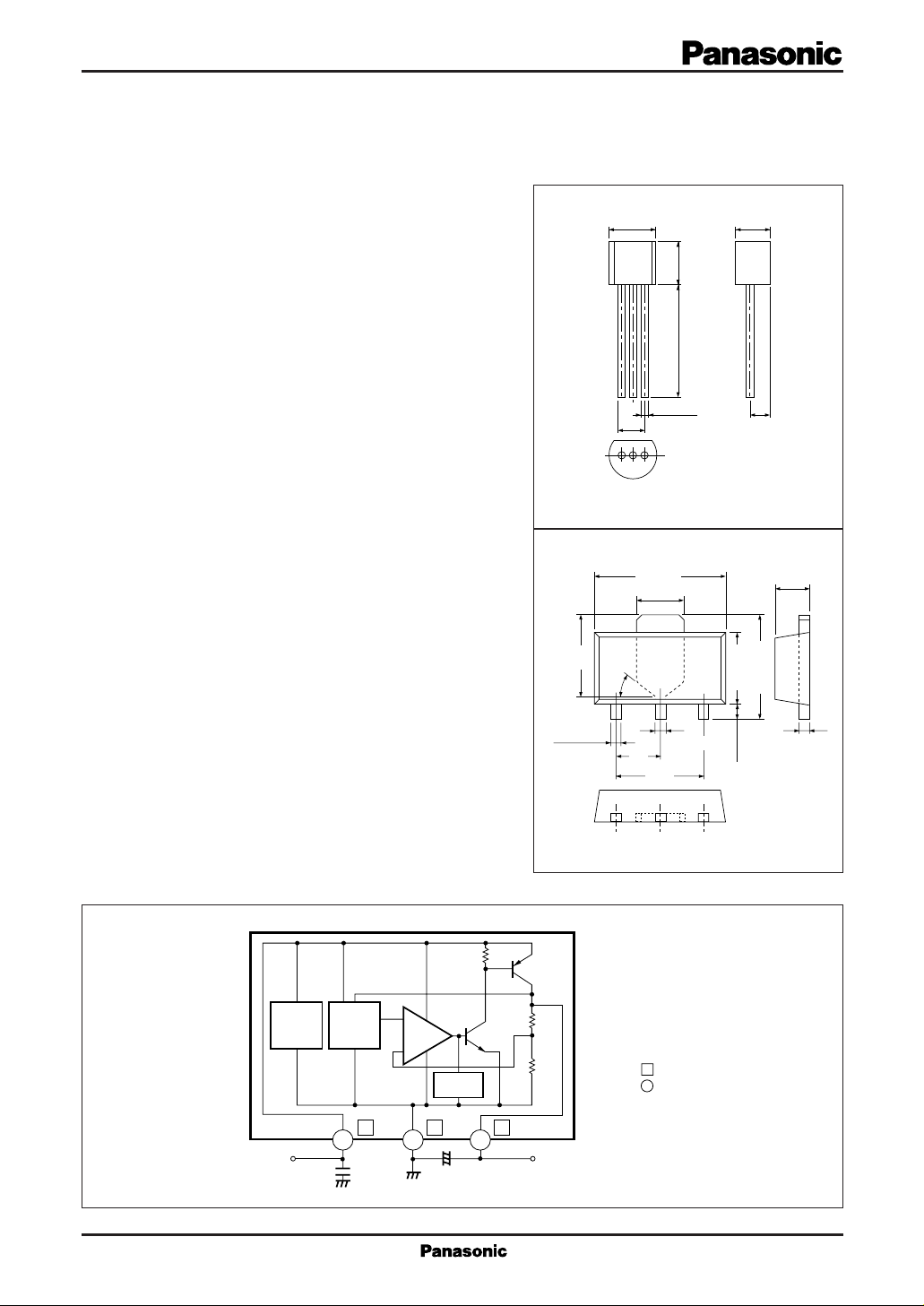
AN8000 Series
AN8000M Series
5.0±0.2
(Bottom View)
TO-92 Plastic Package (SSIP003-P-0000)
2.6
45˚
2.54
321
0.45
4.6max.
1.8max.
+ 0.2
– 0.1
2.3±0.2
2.6max.
Unit:mm
Unit:mm
1.6max.
4.25max.
4.0±0.2
5.1±0.213.5±0.5
1 : Input
2 : Output
3 : GND
■ Block Diagram
V
Starter
I
Voltage
Reference
+
Error
Amp.
–
–
C
Current
Limiter
+
OUT
0.48max.
123
3-pin Mini Power type Plastic Package (TO-243) (HSIP003-P-0000B)
R
2
R
1
1.5
0.58max.
3.0
: TO-92
0.8min.
0.44max.
1 : Output
2 : GND
3 : Input
: TO-243
231
123
V
O
R1=5kΩ
CIN=0.33µF
C
=10µF
OUT
Page 2
■ Absolute Maximum Ratings (Ta=25˚C)
Parameter Symbol Rating
Supply voltage
Supply current
Power dissipation
Operating ambient temperature
Storage temperature
*
Mounting onto the PCB (20 × 20 × 1.7mm glass epoxy copper foil 1 cm2 or more), for AN8000M Series.
AN8000 Series
AN8000M Series
V
I
I
CC
P
D
T
opr
T
stg
20
100
*
650
–30 to+80
–55 to+150
–55 to+125
■ Electrical Characteristics (Ta=25˚C)
AN8002/AN8002M (2V Type)
·
Parameter Symbol Condition min typ max
Output voltage
Line regulation
Load regulation
Minimum I/O voltage difference
Bias current
Ripple rejection ratio
Output noise voltage
Output voltage temperature coefficient
Note1) The specified condition T
=25˚C means that the test should be conducted with each test time reduced (within 10ms) so that
j
REG
REG
V
DIF (min.)
∆V
V
I
RR
V
bias
O
the drift in characteristic value due to a temperature rise at chip junction can be ignored.
Note2) Unless otherwise specified, VI=3V, IO=20mA, CO=10µF
T
=25˚C
O
j
=2.5 to 8V, Tj=25˚C
V
I
IN
=1 to 40mA, Tj=25˚C
I
O
L
=1 to 50mA, Tj=25˚C
I
O
VI=1.9V, IO=20mA, Tj=25˚C
=1.9V, IO=50mA, Tj=25˚C
V
I
I
=0mA, Tj=25˚C
O
V
=3 to 5V, f=120Hz
I
f=10Hz to 100kHz
no
=–30 to+125˚C
T
/Ta
j
1.92
62
10
0.12
74
60
0.1
2
7
Unit
V
mA
mW
˚C
˚C
2.08 V2
40
20 mV
25
0.2
0.3
1
mV/˚C
Unit
mV
mV
V0.06
V
mA0.6
dB
µV
AN8025/AN8025M (2.5V Type)
·
Parameter Symbol Condition min typ max Unit
Output voltage
Line regulation
Load regulation
Minimum I/O voltage difference
Bias current
Ripple rejection ratio
Output noise voltage
Output voltage temperature coefficient
Note1) The specified condition T
V
REG
REG
V
DIF (min.)
bias
V
∆VO/Ta
=25˚C means that the test should be conducted with each test time reduced (within 10ms) so that
j
Tj=25˚C
O
=3 to 8.5V, Tj=25˚C
V
I
IN
IO=1 to 40mA, Tj=25˚C
L
=1 to 50mA, Tj=25˚C
I
O
VI=2.4V, IO=20mA, Tj=25˚C
VI=2.4V, IO=50mA, Tj=25˚C
I
=0mA, Tj=25˚C
O
V
=3.5 to 5.5V, f=120Hz
I
f=10Hz to 100kHz
no
no
=–30 to+125˚C
T
j
the drift in characteristic value due to a temperature rise at chip junction can be ignored.
Note2) Unless otherwise specified, VI=3.5V, IO=20mA, CO=10µF
2.4
60
2.5
12.5
0.12
0.13
2.6 V2.5
50
mV
8
20 mV
mV
25
0.2
0.3
72
65
V0.07
V
mA0.6I
1
dBRR
µVV
mV/˚C
Page 3
■ Electrical Characteristics (Ta=25˚C)
AN8003/AN8003M (3V Type)
·
Parameter Symbol Condition min typ max
Output voltage
Line regulation
Load regulation
Minimum I/O voltage difference
Bias current
Ripple rejection ratio
Output noise voltage
Output voltage temperature coefficient
V
REG
REG
V
DIF (min.)
I
bias
RR
no
∆VO/Ta
O
=25˚C
T
j
IN
=1 to 40mA, Tj=25˚C
I
O
L
=1 to 50mA, Tj=25˚C
I
O
=2.9V, IO=20mA, Tj=25˚C
V
I
=2.9V, IO=50mA, Tj=25˚C
V
I
=0mA, Tj=25˚C
I
O
=4 to 6V, f=120Hz
V
I
f=10Hz to 100kHz
=–30 to+125˚C
T
j
2.88
58
3
9
15
0.12
70
70
Note1) The specified condition Tj=25˚C means that the test should be conducted with each test time reduced (within 10ms) so that
the drift in characteristic value due to a temperature rise at chip junction can be ignored.
Note2) Unless otherwise specified, VI=4V, IO=20mA, CO=10µF
AN8035/AN8035M (3.5V Type)
·
Parameter Symbol Condition min typ max
Output voltage
Line regulation
Load regulation
Minimum I/O voltage difference
Bias current
Ripple rejection ratio
Output noise voltage
Output voltage temperature coefficient
Note1) The specified condition T
V
REG
REG
V
DIF (min.)
bias
V
∆VO/Ta
=25˚C means that the test should be conducted with each test time reduced (within 10ms) so that
j
Tj=25˚C
O
=4 to 9.5V, Tj=25˚C
V
I
IN
IO=1 to 40mA, Tj=25˚C
L
=1 to 50mA, Tj=25˚C
I
O
VI=3.4V, IO=20mA, Tj=25˚C
VI=3.4V, IO=50mA, Tj=25˚C
I
=0mA, Tj=25˚C
O
V
=4.5 to 6.5V, f=120Hz
I
f=10Hz to 100kHz
no
no
=–30 to+125˚C
T
j
3.36
57
3.5
10
20
0.12
69
75
0.2
the drift in characteristic value due to a temperature rise at chip junction can be ignored.
Note2) Unless otherwise specified, VI=4.5V, IO=20mA, CO=10µF
3.12 V3
50
25 mV
30
0.2
0.3
1
mV/˚C0.15
3.64 V3.5
50
30 mV
40
0.2
0.3
1
mV/˚C
Unit
mVVI=3.5 to 9V, Tj=25˚C
mV
mA0.6
µVV
Unit
mV
mV
mA0.6I
µVV
V0.07
V
dB
V0.07
V
dBRR
AN8004/AN8004M (4V Type)
·
Parameter Symbol Condition min typ max
Output voltage
Line regulation
Load regulation
Minimum I/O voltage difference
Bias current
Ripple rejection ratio
Output noise voltage
Output voltage temperature coefficient
Note1) The specified condition T
V
REG
REG
V
DIF (min.)
I
bias
V
∆VO/Ta
=25˚C means that the test should be conducted with each test time reduced (within 10ms) so that
j
Tj=25˚C
O
=4.5 to 10V, Tj=25˚C
V
I
IN
IO=1 to 40mA, Tj=25˚C
L
=1 to 50mA, Tj=25˚C
I
O
VI=3.8V, IO=20mA, Tj=25˚C
VI=3.8V, IO=50mA, Tj=25˚C
I
=0mA, Tj=25˚C
O
V
=5 to 7V, f=120Hz
I
f=10Hz to 100kHz
no
no
=–30 to+125˚C
T
j
the drift in characteristic value due to a temperature rise at chip junction can be ignored.
Note2) Unless otherwise specified, VI=5V, IO=20mA, CO=10µF
3.84
Unit
4.16 V4
3.5
10
20
0.12
56
67
80
0.2
50
mV
30 mV
mV
40
0.2
0.3
mA0.6
1
mV/˚C
V0.07
V
dBRR
µVV
Page 4

■ Electrical Characteristics (Ta=25˚C)
AN8045/AN8045M (4.5V Type)
·
Parameter Symbol Condition min typ max
Output voltage
Line regulation
Load regulation
Minimum I/O voltage difference
Bias current
REG
REG
V
DIF (min.)
V
bias
Ripple rejection ratio
Output noise voltage
Output voltage temperature coefficient
Note1) The specified condition T
=25˚C means that the test should be conducted with each test time reduced (within 10ms) so that
j
V
∆VO/Ta
the drift in characteristic value due to a temperature rise at chip junction can be ignored.
Note2) Unless otherwise specified, VI=5.5V, IO=20mA, CO=10µF
AN8005/AN8005M (5V Type)
·
Parameter Symbol Condition min typ max
Output voltage
Line regulation
Load regulation
Minimum I/O voltage difference
Bias current
REG
REG
V
DIF (min.)
V
bias
Ripple rejection ratio
Output noise voltage
Output voltage temperature coefficient
Note1) The specified condition T
=25˚C means that the test should be conducted with each test time reduced (within 10ms) so that
j
V
∆VO/Ta
the drift in characteristic value due to a temperature rise at chip junction can be ignored.
Note2) Unless otherwise specified, VI=6V, IO=20mA, CO=10µF
Tj=25˚C
O
=5 to 10.5V, Tj=25˚C
V
I
IN
IO=1 to 40mA, Tj=25˚C
L
=1 to 50mA, Tj=25˚C
I
O
VI=4.3V, IO=20mA, Tj=25˚C
VI=4.3V, IO=50mA, Tj=25˚C
I
=0mA, Tj=25˚C
O
V
=5.5 to 7.5V, f=120Hz
I
f=10Hz to 100kHz
no
no
=–30 to+125˚C
T
j
T
=25˚C
O
j
=5.5 to 11V, Tj=25˚C
V
I
IN
IO=1 to 40mA, Tj=25˚C
L
=1 to 50mA, Tj=25˚C
I
O
VI=4.8V, IO=20mA, Tj=25˚C
VI=4.8V, IO=50mA, Tj=25˚C
I
=0mA, Tj=25˚C
O
V
=6 to 8V, f=120Hz
I
f=10Hz to 100kHz
no
no
=–30 to+125˚C
T
j
4.32
54
4.8
52
0.12
0.23
4.5
0.12
0.25
Unit
4.68 V4.5
50
4
11
23
66
85
mV
35 mV
mV
45
0.2
0.3
mA0.7I
1
V0.07
V
dBRR
µVV
mV/˚C
Unit
5.2 V5
50
mV
12
25
64
95
40 mV
mV
50
0.2
0.3
mA0.7I
1
V0.07
V
dBRR
µVV
mV/˚C
AN8006/AN8006M (6V Type)
·
Parameter Symbol Condition min typ max
Output voltage
Line regulation
Load regulation
Minimum I/O voltage difference
Bias current
Ripple rejection ratio
Output noise voltage
Output voltage temperature coefficient
Note1) The specified condition T
V
REG
REG
V
DIF (min.)
bias
V
∆VO/Ta
=25˚C means that the test should be conducted with each test time reduced (within 10ms) so that
j
T
=25˚C
O
j
=6.5 to 12V, Tj=25˚C
V
I
IN
IO=1 to 40mA, Tj=25˚C
L
=1 to 50mA, Tj=25˚C
I
O
VI=5.8V, IO=20mA, Tj=25˚C
VI=5.8V, IO=50mA, Tj=25˚C
I
=0mA, Tj=25˚C
O
V
=7 to 9V, f=120Hz
I
f=10Hz to 100kHz
no
no
=–30 to+125˚C
T
j
the drift in characteristic value due to a temperature rise at chip junction can be ignored.
Note2) Unless otherwise specified, VI=7V, IO=20mA, CO=10µF
5.76
51
5.5
0.13
105
0.3
Unit
6.24 V6
60
mV
13
28
63
45 mV
mV
55
0.2
0.3
mA0.7I
1.2
V0.07
V
dBRR
µVV
mV/˚C
Page 5

■ Electrical Characteristics (Ta=25˚C)
AN8007/AN8007M (7V Type)
·
Parameter Symbol Condition min typ max
Output voltage
Line regulation
Load regulation
Minimum I/O voltage difference
Bias current
REG
REG
V
DIF (min.)
V
bias
Ripple rejection ratio
Output noise voltage
Output voltage temperature coefficient
Note1) The specified condition T
=25˚C means that the test should be conducted with each test time reduced (within 10ms) so that
j
V
∆VO/Ta
the drift in characteristic value due to a temperature rise at chip junction can be ignored.
Note2) Unless otherwise specified, VI=8V, IO=20mA, CO=10µF
AN8008/AN8008M (8V Type)
·
Parameter Symbol Condition min typ max
Output voltage
Line regulation
Load regulation
Minimum I/O voltage difference
Bias current
REG
REG
V
DIF (min.)
V
bias
Ripple rejection ratio
Output noise voltage
Output voltage temperature coefficient
Note1) The specified condition T
=25˚C means that the test should be conducted with each test time reduced (within 10ms) so that
j
V
∆VO/Ta
the drift in characteristic value due to a temperature rise at chip junction can be ignored.
Note2) Unless otherwise specified, VI=9V, IO=20mA, CO=10µF
Tj=25˚C
O
=7.5 to 13V, Tj=25˚C
V
I
IN
IO=1 to 40mA, Tj=25˚C
L
=1 to 50mA, Tj=25˚C
I
O
VI=6.8V, IO=20mA, Tj=25˚C
VI=6.8V, IO=50mA, Tj=25˚C
I
=0mA, Tj=25˚C
O
V
=8 to 10V, f=120Hz
I
f=10Hz to 100kHz
no
no
=–30 to+125˚C
T
j
=25˚C
T
O
j
=8.5 to 14V, Tj=25˚C
V
I
IN
IO=1 to 40mA, Tj=25˚C
L
=1 to 50mA, Tj=25˚C
I
O
VI=7.8V, IO=20mA, Tj=25˚C
VI=7.8V, IO=50mA, Tj=25˚C
I
=0mA, Tj=25˚C
O
V
=9 to 11V, f=120Hz
I
f=10Hz to 100kHz
no
no
=–30 to+125˚C
T
j
6.72
50
7.68
49
6.5
0.13
120
0.35
7.5
0.14
135
0.4
Unit
7.28 V7
70
mV
14
31
62
50 mV
mV
60
0.2
0.3
mA0.7I
1.3
V0.07
V
dBRR
µVV
mV/˚C
Unit
8.32 V8
80
mV
15
34
61
55 mV
mV
65
0.2
0.3
mA0.7I
1.3
V0.07
V
dBRR
µVV
mV/˚C
AN8085/AN8085M (8.5V Type)
·
Parameter Symbol Condition min typ max
Output voltage
Line regulation
Load regulation
Minimum I/O voltage difference
Bias current
Ripple rejection ratio
Output noise voltage
Output voltage temperature coefficient
Note1) The specified condition T
V
REG
REG
V
DIF (min.)
bias
V
∆VO/Ta
=25˚C means that the test should be conducted with each test time reduced (within 10ms) so that
j
T
=25˚C
O
j
=9 to 14.5V, Tj=25˚C
V
I
IN
IO=1 to 40mA, Tj=25˚C
L
=1 to 50mA, Tj=25˚C
I
O
VI=8.3V, IO=20mA, Tj=25˚C
VI=8.3V, IO=50mA, Tj=25˚C
I
=0mA, Tj=25˚C
O
V
=9.5 to 11.5V, f=120Hz
I
f=10Hz to 100kHz
no
no
=–30 to+125˚C
T
j
the drift in characteristic value due to a temperature rise at chip junction can be ignored.
Note2) Unless otherwise specified, VI=9.5V, IO=20mA, CO=10µF
8.16
48
8.3
0.14
140
0.43
Unit
8.84 V8.50
90
mV
16
36
60
60 mV
mV
70
0.2
0.3
mA0.8I
1.4
V0.07
V
dBRR
µVV
mV/˚C
Page 6

■ Electrical Characteristics (Ta=25˚C)
AN8009/AN8009M (9V Type)
·
Parameter Symbol Condition min typ max
Output voltage
Line regulation
Load regulation
Minimum I/O voltage difference
Bias current
REG
REG
V
DIF (min.)
V
bias
Ripple rejection ratio
Output noise voltage
Output voltage temperature coefficient
Note1) The specified condition T
=25˚C means that the test should be conducted with each test time reduced (within 10ms) so that
j
V
∆VO/Ta
the drift in characteristic value due to a temperature rise at chip junction can be ignored.
Note2) Unless otherwise specified, VI=10V, IO=20mA, CO=10µF
AN8010/AN8010M (10V Type)
·
Parameter Symbol Condition min typ max
Output voltage
Line regulation
Load regulation
Minimum I/O voltage difference
Bias current
REG
REG
V
DIF (min.)
V
bias
Ripple rejection ratio
Output noise voltage
Output voltage temperature coefficient
Note1) The specified condition T
=25˚C means that the test should be conducted with each test time reduced (within 10ms) so that
j
V
∆VO/Ta
the drift in characteristic value due to a temperature rise at chip junction can be ignored.
Note2) Unless otherwise specified, VI=11V, IO=20mA, CO=10µF
Tj=25˚C
O
=9.5 to 15V, Tj=25˚C
V
I
IN
IO=1 to 40mA, Tj=25˚C
L
=1 to 50mA, Tj=25˚C
I
O
VI=8.8V, IO=20mA, Tj=25˚C
VI=8.8V, IO=50mA, Tj=25˚C
I
=0mA, Tj=25˚C
O
V
=10 to 12V, f=120Hz
I
f=10Hz to 100kHz
no
no
=–30 to+125˚C
T
j
=25˚C
T
O
j
=10.5 to 16V, Tj=25˚C
V
I
IN
IO=1 to 40mA, Tj=25˚C
L
=1 to 50mA, Tj=25˚C
I
O
VI=9.8V, IO=20mA, Tj=25˚C
VI=9.8V, IO=50mA, Tj=25˚C
I
=0mA, Tj=25˚C
O
V
=11 to 13V, f=120Hz
I
f=10Hz to 100kHz
no
no
=–30 to+125˚C
T
j
8.64
47
9.6
46
0.14
150
0.45
0.14
165
0.5
Unit
9.36 V9
100
9
17
37
59
mV
70 mV
mV
75
0.2
0.3
mA0.8I
1.4
V0.07
V
dBRR
µVV
mV/˚C
Unit
10.4 V10
100
10
18
40
58
mV
75 mV
mV
85
0.2
0.3
mA0.8I
1.4
V0.07
V
dBRR
µVV
mV/˚C
■ Applica tion Circuit
The AN8000/AN8000M series has IC internal gain increased in order to improve
performance. When the power line on the output side is long, use a capacitor of
10µF.
For the capacitor on the output side, attach it as close to the IC as possible.
When using at a low temperature, it is recommended to use the capacitors with
low internal impedance (for example, tantalum capacitor) for output capacitors.
V
in
0.33µF
AN8000
AN8000M
V
out
+
10µF
–
Page 7

■ Characteristic Curve
PD –Ta (AN8000 Series)
800
700
600
(mW)
D
500
400
300
200
100
Power Dissipation P
0
0 20406080
80
70
60
50
40
30
Ripple Rejection Ratio RR (dB)
50 100 300
Ambient Temperature Ta (˚C)
1k 3k
500
Frequency f (Hz)
100 120 140 160
RR– f
5k
10k 30k
AN8005
50k
800
700
600
(mW)
D
500
400
300
200
100
Power Dissipation P
(V)
O
Output Voltage V
100k
PD –Ta (AN8000M Series)
Mounting onto PCB
20 × 20 × 7mm
Glass Epoxy PCB,
()
Copper foil 1cm
0
0 20406080
100 120 140 160
Ambient Temperature Ta (˚C)
VO –V
12
CO=10µF
=0mA
I
O
10
8
6
4
2
0
0 5 10 15 20
I
Input Voltage VI (V)
AN8010/M
AN8005/M
AN8002/M
2
or more
VO – I
5.3
5.2
(V)
O
5.1
5.0
4.9
Output Voltage V
4.8
4.7
0 102030405060708090100
O
AN8005
=6V
V
I
=10µF
C
O
Output Current VO (mA)
VO –Ta
5.3
5.2
(V)
O
5.1
5.0
4.9
Output Voltage V
4.8
4.7
–40 –20 0 20 40 60 80 100 120 140 160
Ambient Temperature Ta (˚C)
AN8005
=6V
V
I
=10µF
C
O
=0mA
I
O
 Loading...