

Page 1
Voltage Regulators
AN8049SH
1.8-volt 3-channel step-up, step-down, and polarity inverting
DC-DC converter control IC
■ Overview
The AN8049SH is a three-channel PWM DC-DC
converter control IC that features low-voltage operation.
This IC can form a power supply that provides two stepup outputs and one step-down or polarity inverted output
with a minimal number of external components. The
AN8049SH features the ability to operate from a supply
voltage as low as 1.8 V, and thus can be operated from
two dry-batteries.
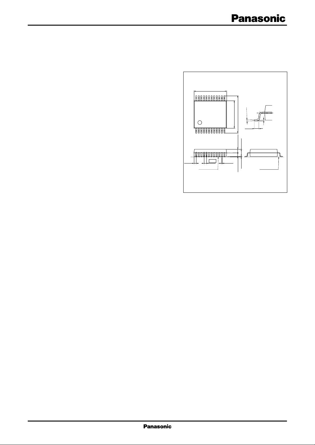
6.5±0.3
24 13
+0.10
5.5±0.3
7.5±0.3
(0.50)
112
0.65±0.100.65±0.10
1.5±0.20.1±0.1
– 0.05
0.15
Unit : mm
0° to 10°
■ Features
(0.50)
0.50
Seating plane
0.2±0.1
• Wide operating supply voltage range: 1.8 V to 14 V
• High-precision reference voltage circuit
—V
REF
pin voltage: ±1%
SSOP024-P-0300A
— Error amplifier: ±1.5%
• Surface mounting package for miniaturized and thinner power supplies
Package: SSOP-24D
0.5-mm lead pitch
7.8 mm × 6.8 mm × t 1.9 mm
• Supports control over a wide output frequency range: 20 kHz to 1 MHz
• On/off (sequence control) pins provided for each channel for easy sequence control setup
• The negative supply error amplifier supports 0-volt input.
Common-mode input voltage range: − 0.1 V to V
−1.4 V
CC
This allows the number of external components to be reduced by two resistors.
• Fixed duty factor: 86%
However, the duty can be adjusted to anywhere from 0% to 100% with an external resistor.
• Timer latch short-circuit protection circuit (charge current: 1.1 µA typical)
• Low input voltage malfunction prevention circuit (U.V.L.O.) (operation start voltage: 1.67 V typical)
• Standby function (active-high control input, standby mode current: 1 µA maximum)
• Alternate package versions also available.
Part No.: AN8049FHN
Package: QFN-24
0.5-mm lead pitch
5.4 mm × 4.4 mm × t 0.8 mm
Seating plane
■ Applications
• Electronic equipment that requires a power supply system
1
Page 2
AN8049SH Voltage Regulators
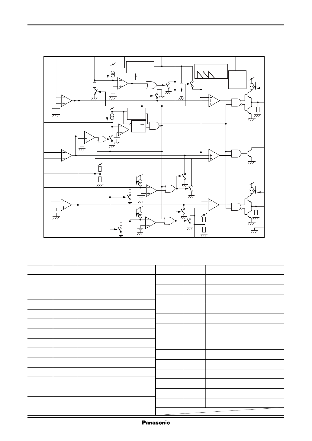
■ Block Diagram
S.C.P.
FB3
IN+3
IN−3
DT3
CTL3
IN-123FB124CTL1
Error
amplifier 1
1.26 V
1
20
Error
amplifier 2
18
S.C.P. comp.
19
2
5
Error
amplifier 3
1.26 V
21
22
V
7
1.1 µA
0.9 V
REF
20 kΩ
V
CC
1.1 µA
44 kΩ56 kΩ
20 kΩ
CC
V
16
Reference voltage
supply
1.26 V
U.V.L.O.
1.26 V
1.1 µA
1.1 µA
20 kΩ
6
V
REF
(Allowance: ±1%)
R
Q
S
Latch
1.26 V
1.26 V
REF
V
9
1.26 V
4
DT1
45 kΩ
55 kΩ
3
OSC
17
Sawtooth wave generator
0.7 V
0.3 V
PWM1
PWM3
PWM2
V
REF
45 kΩ
55 kΩ
Off
8
On/off
control
V
CC
V
CC
11
RB1
12
OUT1
27 kΩ
15
OUT3
10
RB2
13
OUT2
27 kΩ
14
GND
IN−2
FB2
■ Pin Descriptions
Pin No. Symbol Description
1 S.C.P. Connection for the capacitor
2 DT3 Channel 3 soft start setting
3 DT2 Channel 2 soft start setting
4 DT1 Channel 1 soft start setting
5 CTL3 Channel 3 on/off control
6 CTL2 Channel 2 on/off control
7 CTL1 Channel 1 on/off control
8 Off On/off control
9V
10 RB2 Connection for the OUT2
11 RB1 Connection for the OUT1
2
that provides the shortcircuit protection circuit time
constant
Reference voltage output
REF
block output source current
setting resistor
block output source current
setting resistor
CTL2
DT2
Pin No. Symbol Description
12 OUT1 OUT1 block push-pull output
13 OUT2 OUT2 block push-pull output
14 GND Ground
15 OUT3 OUT3 block open-collector output
16 V
CC
Supply voltage
17 OSC Oscillator circuit timing resistor and
capacitor connection
18 IN+3 Error amplifier 3 noninverting input
19 IN−3 Error amplifier 3 inverting input
20 FB3 Error amplifier 3 output
21 IN−2 Error amplifier 2 inverting input
22 FB2 Error amplifier 2 output
23 IN−1 Error amplifier 1 inverting input
24 FB1 Error amplifier 1 output
Page 3
Voltage Regulators AN8049SH
■ Absolute Maximum Ratings
Parameter Symbol Rating Unit
Supply voltage V
Off pin allowable application V
CC
OFF
voltage
CTL pin allowable application V
CTL
voltage
Error amplifier input pin V
allowable application voltage
*
Supply current I
OUT1 and OUT2 pin output I
2
IN
CC
SO(OUT)
source current
OUT3 pin output current I
1
Power dissipation
*
Operating temperature T
Storage temperature T
Note) 1. Do not apply external currents or voltages to any pins not specifically mentioned. For circuit currents, '+' denotes current
flowing into the IC, and '−' denotes current flowing out of the IC.
2. Items other than the storage temperature, operating temperature, and power dissipation are all stipulated for an ambient
temperature Ta = 25°C.
3.*1: Ta = 85°C. See the "Application Notes" for details on the relationship between IC power dissipation and the ambient
temperature.
2: When VCC < 6 V, the following condition must hold: V
*
O
P
D
opr
stg
14.2 V
14.2 V
VCC − 0.2 V
6V
mA
−50 mA
+50 mA
146 mW
−30 to +85 °C
−55 to +125 °C
= V
IN−1
= VCC − 0.2 V.
IN−2
■ Recommended Operating Range
Parameter Symbol Range Unit
Off pin application voltage V
OUT1 and OUT2 pin output source current I
OUT3 pin output current I
Timing resistance R
Timing capacitance C
Oscillator frequency f
Short-circuit protection time-constant setting capacitance C
Output current setting resistance R
OFF
SO(OUT)
O
T
T
OUT
SCP
B
0 to 14 V
−40 to −1mA
40 (max.)
3 to 33 kΩ
100 to 10 000 pF
20 to 1 000 kHz
1 000 (min.) pF
750 to 15 000 Ω
3
Page 4
AN8049SH Voltage Regulators
■ Electrical Characteristics at V
= 2.4 V, C
CC
Parameter Symbol Conditions Min Typ Max Unit
Reference voltage block
Reference voltage V
Line regulation with input fluctuation
REFIREF
Line V
Load regulation Load I
U.V.L.O. block
Circuit operation start voltage V
UON
Error amplifier 1 block
Input threshold voltage 1 V
Input bias current 1 I
High-level output voltage 1 V
Low-level output voltage 1 V
Output source current 1 I
Output sink current 1 I
TH1
B1
EH1
EL1
SO(FB)1
SI(FB)1
Error amplifier 2 block
Input threshold voltage 2 V
Input bias current 2 I
High-level output voltage 2 V
Low-level output voltage 2 V
Output source current 2 I
Output sink current 2 I
TH2
B2
EH2
EL2
SO(FB)2
SI(FB)2
Error amplifier 3 block
Input offset voltage V
Common-mode input voltage range V
Input bias current 3 I
High-level output voltage 3 V
Low-level output voltage 3 V
Output source current 3 I
Output sink current 3 I
IO
ICR
B3
EH3
EL3
SO(FB)3
SI(FB)3
Oscillator block
Oscillator frequency f
OUT
= 0.1 µF, Ta = 25°C
REF
= − 0.1 mA 1.247 1.26 1.273 V
= 1.8 V to 14 V 220mV
CC
= − 0.1 mA to −1 mA −20 −3 mV
REF
1.59 1.67 1.75 V
1.241 1.26 1.279 V
0.1 0.2 µA
1.0 1.2 1.4 V
0.2 V
−38 −31 −24 µA
0.5 mA
1.241 1.26 1.279 V
0.1 0.2 µA
1.0 1.2 1.4 V
0.2 V
−38 −31 −24 µA
0.5 mA
−6 6mV
− 0.1 V
CC
V
−1.4
− 0.6 − 0.3 µA
1.0 1.2 1.4 V
0.2 V
−38 −31 −24 µA
0.5 mA
RT = 7.5 kΩ, CT = 680 pF 170 190 210 kHz
4
Page 5
Voltage Regulators AN8049SH
■ Electrical Characteristics at V
Parameter Symbol Conditions Min Typ Max Unit
Output 1 block
Output duty factor 1 Du
High-level output voltage 1 V
Low-level output voltage 1 V
Output source current 1 I
Output sink current 3 I
Pull-down resistor 1 R
Output 2 block
Output duty factor 2 Du
High-level output voltage 2 V
Low-level output voltage 2 V
Output source current 2 I
Output sink current 2 I
Pull-down resistor 2 R
Output 3 block
Output duty factor 3 Du
Output saturation voltage V
Output leakage current I
Short-circuit protection circuit block
Input standby voltage V
Input threshold voltage V
Input latch voltage V
Charge current I
On/off control block
Input threshold voltage V
CTL block
Input threshold voltage V
Charge current I
Whole Device
Average consumption current I
Standby mode current I
= 2.4 V, C
CC
RT = 7.5 kΩ, CT = 680 pF 80 86 92 %
1
OH1IO
OL1IO
SO(OUT)1VO
SI(OUT)1VO
O1
RT = 7.5 kΩ, CT = 680 pF 80 86 92 %
2
OH2IO
OL2IO
SO(OUT)2VO
SI(OUT)2VO
O2
RT = 7.5 kΩ, CT = 680 pF 80 86 92 %
3
O(SAT)IO
V13 = 14 V 1 µA
OLE
STBY
THPC
IN
V
CHG
ON(TH)
THCTL
V
CTL
CC(OFF)RB
CC(SB)
= 0.1 µF, Ta = 25°C (continued)
REF
= −10 mA, RB = 1 kΩ VCC −1 V
= 10 mA, RB = 1 kΩ0.2 V
= 0.7 V, RB = 1 kΩ−34 −29 −24 mA
= 0.7 V, RB = 1 kΩ 40 mA
17 27 37 kΩ
= −10 mA, RB = 1 kΩ VCC −1 V
= 10 mA, RB = 1 kΩ0.2 V
= 0.7 V, RB = 1 kΩ−34 −29 −24 mA
= 0.7 V, RB = 1 kΩ 40 mA
17 27 37 kΩ
= 40 mA 0.5 V
0.1 V
0.8 0.9 1.0 V
0.1 V
= 0 V −1.43 −1.1 − 0.77 µA
SCP
0.6 0.9 1.2 V
1.07 1.26 1.45 V
= 0 V −1.43 −1.1 − 0.77 µA
CTL
= 9.1 kΩ, duty = 50% 4.2 5.5 mA
1 µA
5
Page 6
AN8049SH Voltage Regulators
■ Electrical Characteristics at Ta = 25°C (continued)
•
Design reference data
Note: The characteristics listed below are reference values related to the IC design and are not guaranteed.
Parameter Symbol Conditions Min Typ Max Unit
Reference voltage block
V
temperature characteristics V
REF
RFEdTTa
Error amplifier 1 block
VTH temperature characteristics V
Open loop gain 1 A
THdT1Ta
V1
Error amplifier 2 block
VTH temperature variation V
Open loop gain 2 A
THdT2
V2
Error amplifier 3 block
Open loop gain 3 A
V3
Oscillator block
Frequency supply voltage f
DV
characteristics RT = 7.5 kΩ, CT = 680 pF
Frequency temperature f
DT
characteristics RT = 7.5 kΩ, CT = 680 pF
Short-circuit protection circuit block
Comparator threshold voltage V
THL
On/off control block
Off pin current I
OFF
= −30°C to +85°C 1 %
= −30°C to +85°C 1.5 %
80 dB
1.5 %
80 dB
80 dB
VCC = 1.8 V to 14 V 1 %
Ta = −30°C to +85°C 3 %
1.26 V
V
= 5 V 38 µA
OFF
6
Page 7
Voltage Regulators AN8049SH
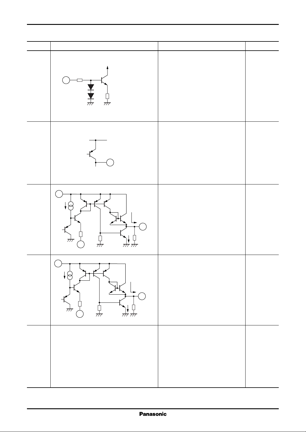
■ Terminal Equivalent Circuits
Pin No. Equivalent circuit Description I/O
1 S.C.P.: O
2 DT3: I
3 DT2: I
4 DT1: I
V
CC
1.5 kΩ
2
4
3
1.1 µA
1
44 kΩ
46 kΩ
45 kΩ
55 kΩ
45 kΩ
55 kΩ
1.26 V
9
9
9
Latch
S
R
20 17
22 17
24 17
Q
Output
shutoff
PWM3
PWM2
PWM1
Connection for the capacitor that sets
the timer latch short-circuit protection
circuit time constant. Use a capacitor
with a value of 1 000 pF or higher.
The charge current I
is 1.1 µA
CHG
typical.
Sets the channel 3 soft start time.
Set the time by connecting a capacitor
between this pin and ground.
(See the "Application Notes, [7]" section.)
Note that although the channel 3
maximum on duty is set internally to
86%, the maximum on duty can be
adjusted by connecting resistors between
this pin and ground, and between this
pin and the V
pin. (See the "Application
REF
Notes, [6]" section.)
Sets the channel 2 soft start time.
Set the time by connecting a capacitor
between this pin and ground.
(See the "Application Notes, [7]" section.)
Note that although the channel 2
maximum on duty is set internally to
86%, the maximum on duty can be
adjusted by connecting resistors
between this pin and ground, and
between this pin and the V
REF
pin.
(See the "Application Notes, [6]" section.)
Sets the channel 1 soft start time.
Set the time by connecting a capacitor
between this pin and ground.
(See the "Application Notes, [7]" section.)
Note that although the channel 1
maximum on duty is set internally to
86%, the maximum on duty can be
adjusted by connecting resistors
between this pin and ground, and
between this pin and the V
REF
pin.
(See the "Application Notes, [6]" section.)
7
Page 8
AN8049SH Voltage Regulators
■ Terminal Equivalent Circuits (continued)
Pin No. Equivalent circuit Description I/O
5 CTL3: I
Controls the on/off state of channel 3. A
delay can be provided in the power supply
V
CC
20 kΩ
1.1 µA
High
Channel 3
1.26 V
output operation
5
6 CTL2: I
V
CC
20 kΩ
1.1 µA
High
Channel 2
1.26 V
output operation
6
7 CTL1: I
V
CC
20 kΩ
1.1 µA
High
Channel 1
1.26 V
output operation
7
turn-on start time by connecting a capacitor
between this pin and ground.
(See the "Application Notes, [9]" section.)
t
= 1.26 (V) × C
DLY3
(µF)/1.1 (µA) (s)
CTL3
This pin can also be used to control the
on/off state with an external signal. In that
case, the allowable input voltage range is
from 0 V to V
. Note that during
CC
U.V.L.O. and timer latch operation, this
pin is connected to ground through a
20 kΩ resistor.
Controls the on/off state of channel 2.
A delay can be provided in the power
supply turn-on start time by connecting
a capacitor between this pin and
ground.
(See the "Application Notes, [9]" section.)
t
= 1.26 (V) × C
DLY2
(µF)/1.1 (µA) (s)
CTL2
This pin can also be used to control the
on/off state with an external signal.
In that case, the allowable input voltage
range is from 0 V to V
. Note that
CC
during U.V.L.O. and timer latch operation,
this pin is connected to ground through a
20 kΩ resistor.
Controls the on/off state of channel 1.
A delay can be provided in the power
supply turn-on start time by connecting
a capacitor between this pin and
ground. (See the "Application Notes, [9]"
section.)
t
= 1.26 (V) × C
DLY1
(µF)/1.1 (µA) (s)
CTL1
This pin can also be used to control the
on/off state with an external signal.
In that case, the allowable input voltage
range is from 0 V to V
. Note that
CC
during U.V.L.O. and timer latch operation,
this pin is connected to ground through a
20 kΩ resistor.
8
Page 9
Voltage Regulators AN8049SH
■ Terminal Equivalent Circuits (continued)
Pin No. Equivalent circuit Description I/O
8 Off: I
Start and stop of
internal circuits.
8
100 kΩ
9V
V
CC
9
10 RB2: I
16
I
SO(OUT)2
13
10
200 Ω
I
SI(OUT)2
30 kΩ
Controls the on/off state.
When the input is high: normal
operation
(V
> 1.2 V)
OFF
When the input is low: standby mode
(V
< 0.6 V)
OFF
In standby mode, the total current
consumption is held to under 1 µA.
:O
REF
Outputs the internal reference voltage.
The reference voltage is 1.26 V
(allowance: ±1%) when V
2.4 V and I
is − 0.1 mA. Insert a
REF
CC
is
capacitor of at least 0.1 µF between
V
and ground for phase
REF
compensation.
Connection for a resistor that sets the
channel 2 output current.
Use a resistor in the range 750 Ω to
15 kΩ.
11 RB1: I
16
Connection for a resistor that sets the
channel 1 output current.
I
SO(OUT)1
Use a resistor in the range 750 Ω to
15 kΩ.
12
11
200 Ω
I
SI(OUT)1
30 kΩ
12 See pin 11. OUT1: O
Push-pull output.
The absolute maximum rating for the
output source current is −50 mA.
The output source current is set by the
external resistor connected to the RB1
pin.
9
Page 10

AN8049SH Voltage Regulators
■ Terminal Equivalent Circuits (continued)
Pin No. Equivalent circuit Description I/O
13 See pin 10. OUT2: O
Push-pull output.
The absolute maximum rating for the
output source current is −50 mA.
The output source current is set by the
external resistor connected to the RB2
pin.
14 GND:
14
Ground
15 OUT3: O
16 VCC:
17 OSC: O
18 IN+3: I
19 IN−3: I
16
16
V
CC
Latch
S
R
0.2 V
17
16
100 Ω 100 Ω
15
Open-collector output.
The absolute maximum rating for the
output current is +50 mA.
Power supply.
Provide the oprating supply voltage in
the range 1.8 V to 14 V.
Connection for the capacitor and
resistor that determine the oscillator
frequency. Use a capacitor in the range
Q
1819
100 pF to 1 000 pF and a resistor in
the range 3 kΩ to 33 kΩ. Use an
oscillator frequency in the range
20 kHz to 1 MHz.
Noninverting input to the error
amplifier 3.
Inverting input to the error amplifier 3.
20 FB3: O
18
19
10
9
31 µA
0.5 mA
OSC
20
PWM3
Output from the error amplifier 3.
This circuit can provide a source
current of −31 µA or a sink current of
0.5 mA (minimum).
Page 11

Voltage Regulators AN8049SH
■ Terminal Equivalent Circuits (continued)
Pin No. Equivalent circuit Description I/O
21 IN−2: I
22 FB2: O
21
21
16
1.5 kΩ
16
31 µA
OSC
1.26 V
PWM2
Inverting input to the error amplifier 2.
Output from the error amplifier 2.
This circuit can provide a source
current of −31 µA or a sink current of
0.5 mA (minimum).
1.19 V
23 IN−1: I
16
23
1.5 kΩ
24 FB1: O
16
23
1.19 V
0.5 mA
min.
31 µA
OSC
0.5 mA
min.
22
1.26 V
24
PWM1
Inverting input to the error amplifier 1.
Output from the error amplifier 1.
This circuit can provide a source
current of −31 µA or a sink current of
0.5 mA (minimum).
11
Page 12

AN8049SH Voltage Regulators
■ Usage Notes
[1] Allowable power dissipation
1. Since the power dissipation (P) in this IC increases proportionally with the supply voltage, applications must be
careful to operate so that the loss does not exceed the allowable power dissipation, PD, for the package. See the P
Ta curve.
Reference formula:
P = (VCC −V
< P
D
V
BEQ1
I
SO(OUT)1
Du
1
V
BEQ2
I
SO(OUT)2
Du
2
V
O(SAT)3
I
OUT3
Du
3
I
CC
2. If the IC is shorted to ground, shorted to VCC, or inserted incorrectly, either the device itself or peripheral
components will be destroyed.
BEQ1
) × I
SO(OUT)1
× Du1+ (VCC −V
BEQ2
) × I
SO(OUT)2
× Du2+V
O(SAT)3
× I
: The voltage between the base and emitter of the channel 1 npn transistor
: The OUT1 pin output source current
(This is set by the resistor connected to the RB1 pin. When R
is 1 kΩ, I
B
maximum.)
: The output 1 on-duty
: The voltage between the base and emitter of the channel 2 npn transistor
: The OUT2 pin output source current
(This is set by the resistor connected to the RB2 pin. When R
is 1 kΩ, I
B
maximum.)
: The output 2 on-duty
: The OUT3 pin saturation voltage (0.5 V maximum when I
: The OUT3 pin current (This will be {VCC − V
BEQ3
− V
OUT3
O(SAT)3
is 40 mA.)
}/RO3.)
: The output 3 on-duty
: The VCC pin current
× Du3+VCC × I
OUT3
SO(OUT)1
SO(OUT)2
CC
will be 34 mA,
will be 34 mA,
D
[2] Allowable V
ripple due to the switching transistor being turned on and off can cause this IC's U.V.L.O. circuit, which is
V
CC
biased by V
ripple
CC
, to operate incorrectly, and can cause the S.C.P. capacitor charging operation to fail to start when the
CC
output is shorted.
The figure shows the allowable range for V
ripple filter in the V
line or by inserting a capacitor between the IC GND and VCC pins and locating that capacitor
CC
ripple. Applications should reduce VCC ripple either by inserting a
CC
as close to the IC as possible.
Note that the allowable range shown here is the result of testing the IC independently, and that the allowable range
may differ depending on the actual system of the power supply circuit. Also note that this allowable range is a design
target, and is not guaranteed by testing of all samples.
Allowable V
10 M
Allowable range
when V
is 3 V.
1 M
100 k
Ripple frequency (Hz)
10 k
012345678
CC
VCC ripple voltage VCC(AC) (V[p-p])
ripple
CC
Allowable range
when V
is 10 V.
CC
12
Page 13

Voltage Regulators AN8049SH
■ Usage Notes (continued)
[3] Notes on MOS drive
Since the AN8049SH channel 1 and 2 output circuits were designed to drive bipolar transistors, the following points
require care if this device is used to drive n-channel MOS transistors directly.
1. Use an n-channel MOS transistor with a low input capacitance.
The AN8049SH is designed to drive bipolar transistors, and adopts a circuit structure that can provide a constant-current (50 mA maximum) output source current.
Furthermore, it has a sink current capacity of 80 mA maximum. This means that designs must be concerned about
increased loss due to longer rise- and fall-times. If a problem occurs, an inverter may be inserted as shown in figure
1 to provide amplification.
V
IN
OUT1/2
Figure 1. Output boosting circuit
V
OUT
2. Use an n-channel MOS transistor with a low gate-threshold voltage.
Since the AN8049SH OUT1 and OUT2 pin high-level
output voltage is V
− 1.0 V (minimum), low VT MOS
CC
transistors with an adequately low on-resistance must be
used. Also, if a large V
is required, one solution is to use
GS
a transformer as shown in figure 2, and apply a voltage that
is twice the input voltage to the IC's V
CC
pin.
■ Application Notes
[1] SSOP024-P-0300A package power dissipation
P
700
658
600
500
(mW)
D
400
366
300
263
Power dissipation P
200
146
100
Glass epoxy printed circuit board
(75 × 75 × t1.6 mm
R
P
T
D
a
= 152°C/W
th(j−a)
= 658 mW(25°C)
D
Independent IC
without a heat sink
R
th(j−a)
P
D
OUT1/2
3
)
= 273°C/W
= 366 mW(25°C)
V
IN
V
CC
V
OUT
VCC ≈ 2 × VIN−VD
Figure 2. Gate drive voltage boosting
technique
0
0 25 50 75 85 100 125
Ambient temperature Ta (°C)
13
Page 14

AN8049SH Voltage Regulators
■ Application Notes (continued)
[2] Main characteristics
Timing capacitance Oscillator frequency
1M
RT = 3 kΩ
(Hz)
100k
OUT
f
10k
10p 1n 10n
RT = 7.5 kΩ
RT = 33 kΩ
CT (F)
DT3 pin voltage Maximum on-duty
100
90
80
70
60
(%)
50
3
Du
40
30
20
10
0
0.2 0.3 0.4 0.5 0.6 0.7 0.8
f
OSC
95
f = 190 kHz
f = 1 MHz
(V)
V
DT3
Maximum output duty
= 7.5 kΩ)
(R
T
DT1 and DT2 pin voltage Maximum on-duty
100
90
80
70
60
(%)
50
Du
40
30
20
10
0
0.2 0.3 0.4 0.5 0.6 0.7 0.8
f
Maximum output duty
OSC
95
90
(%)
3
, Du
85
2
, Du
1
Du
80
75
Maximum output duty
f
OSC
95
(R
T
= 33 kΩ)
(R
T
f = 190 kHz
V
DT
= 3 kΩ)
f
(Hz)
OSC
(V)
f = 1 MHz
Du1 , Du
Du
3
2
1M100k10k
14
(%)
3
, Du
2
, Du
1
Du
Du
Du
(%)
3
, Du
2
, Du
1
Du
90
Du
85
80
75
90
85
f
OSC
Du1 , Du
(Hz)
80
75
Du
3
2
1M100k10k
2
3
1
1M100k10k
(Hz)
f
OSC
Page 15

Voltage Regulators AN8049SH
■ Application Notes (continued)
[2] Main characteristics (continued)
(mA)
SO(OUT)
I
−10
−20
−30
−40
−50
−60
−70
−80
0
VCC = 1.8 V
2.4 V
8 V
14 V
I
R
B
SO(OUT)
R
B
100k10k1k100
(Ω)
(mA)
SI(OUT)
I
100
90
80
70
60
50
40
30
20
10
0
RB I
SI(OUT)
R
B
VCC = 14 V
8 V
1.8 V , 2.4 V
100k10k1k100
(Ω)
15
Page 16

AN8049SH Voltage Regulators
■ Application Notes (continued)
[3] Timing charts
pin voltage
V
CC
waveform
1.67 V
Output short
1.26 V
S.C.P. pin
voltage
waveform
V
CC
1.26 V
0 V
CTL pin
voltage
waveform
FB OSC DT
OUT1/2 pin
voltage waveform
Totem pole circuit output
OUT3 pin
voltage waveform
Open-collector output
OSC
16
Page 17

Voltage Regulators AN8049SH
■ Application Notes (continued)
[4] Function descriptions
1. Reference voltage block
This circuit is composed of a band gap circuit, and outputs a 1.26 V (typical) reference voltage that is
temperature compensated to a precision of ±1%. This reference voltage is stabilized when the supply voltage is 1.8
V or higher. This reference voltage is used by error amplifiers 1 and 2.
2. Triangular wave generator
This circuit generates a triangular wave like a
sawtooth with a peak of 0.7 V and a trough of 0.2
V using a capacitor C
resistor R
connected to the OSC1 pin (pin 17). The
T
(for the time constant) and
T
oscillator frequency can be set to an arbitrary value
by selecting appropriate values for the external capacitor C
and resistor RT. This IC can use an
T
oscillator frequency in the range 20 kHz to 1 MHz.
The triangular wave signal is provided to the
noninverting input of the PWM comparator in each
channel internally to the IC. Use the formulas below for rough calculation of the oscillator frequency.
t
2
Discharge
Rapid charge
t
1
T
Figure 1. Triangular oscillator waveform
V
OSCH
≈ 0.7 V
V
OSCL
≈ 0.2 V
f
OSC
≈ −
C
× RT × ln
T
1
V
V
≈ 0.8 ×
OSCL
OSCH
1
CT × R
(Hz)
T
Note, however, that the above formulas do not take the rapid charge time, overshoot, and undershoot into
account. See the experimentally determined graph of the oscillator frequency vs. timing capacitance value provided in the main characteristics section.
3. Error amplifier 1
V
FB1
IN−1
OUT1
24
Error
amplifier1
23
= 1.26 ×
1.26 V
R
+
1
R
To the PWM
comparator input
R
2
2
This circuit is an npn-transistor input error
amplifier that detects and amplifies the DC-DC
converter output voltage, and inputs that signal to
a PWM comparator. The 1.26 V internal reference
voltage is applied to the noninverting input. Arbitrary gain and phase compensation can be set up
by inserting a resistor and capacitor in series between the FB1 pin (pin 24) and the IN−1 pin (pin
23). The output voltage V
can be set using the
OUT1
circuit shown in the figure.
R1
R2
V
OUT1
Figure 2. Connection method of error amplifier 1
(Step-up output)
17
Page 18

AN8049SH Voltage Regulators
■ Application Notes (continued)
[4] Function descriptions (continued)
V
FB2
IN−2
OUT2
22
Error
amplifier2
21
= 1.26 ×
1.26 V
R
+
1
R
To the PWM
comparator input
R
2
2
4. Error amplifier 2
This circuit is an npn-transistor input error
amplifier that detects and amplifies the DC-DC
converter output voltage and inputs that signal to
a PWM comparator. The 1.26 V internal reference
R1
V
OUT2
voltage is applied to the noninverting input. Arbitrary gain and phase compensation can be set up
by inserting a resistor and capacitor in series between the FB2 pin (pin 22) and the IN−2 pin (pin
21). The output voltage V
can be set using the
OUT2
R2
circuit shown in the figure.
Figure 3. Connection method of error amplifier 2 (Step-up output)
5. Error amplifier 3
This circuit is an pnp-transistor input error amplifier that detects and amplifies the DC-DC converter output
voltage and inputs that signal to a PWM comparator. Arbitrary gain and phase compensation can be set up by
inserting a resistor and capacitor in series between the FB3 pin (pin 20) and the IN−3 pin (pin 19). The output voltage
V
can be set using the circuit shown in the figure.
OUT3
Step-down output Inverting output
R1
R2
FB3
20
V
V
OUT3
REF
V
R3
R4
OUT3
=
R
R
2
1+R2
IN−3
IN+3
×
Error
amplifier3
18
19
R
3+R4
R
4
× V
To the PWM
comparator input
REF
R1
R2
V
V
REF
OUT3
V
FB3
OUT3
IN+3
IN−3
= −V
20
Error
amplifier3
18
19
REF
×
To the PWM
comparator input
R
2
R
1
Figure 4. Connection method of error amplifier 3
6. Timer latch short-circuit protection circuit
This circuit protects the external main switching elements, flywheel diodes, choke coils, and other components
against degradation or destruction if an excessive load or a short circuit of the power supply output continues for
longer than a certain fixed period.
The timer latch short-circuit protection circuit detects the output of the error amplifiers. If the DC-DC converter
output voltage drops and an FB pin (pins 20, 22, or 24) voltage exceeds 0.9 V, the S.C.P. comparator outputs a low
level and the timer circuit starts. This starts charging the external protection circuit delay time capacitor.
If the error amplifier output does not return to the normal voltage range before that capacitor reaches 1.26 V,
the latch circuit latches, the output drive transistors are turned off, and the dead-time is set to 100%. (See the "[5]
Time constant setup for the timer latch short-circuit protection circuit" section later in this document.)
18
Page 19

Voltage Regulators AN8049SH
■ Application Notes (continued)
[4] Function descriptions (continued)
7. Low input voltage malfunction prevention circuit (U.V.L.O.)
This circuit protects the system against degradation or destruction due to incorrect control operation when the
power supply voltage falls during power on or power off.
The low input voltage malfunction prevention circuit detects the internal reference voltage that changes with
the supply voltage level. While the supply voltage is rising, this circuit cuts off the output drive transistor until the
reference voltage reaches 1.67 V. It also sets the dead-time to 100 % and at the same time holds the S.C.P. pin (pin
1) and the DT pins (pins 2, 3, and 4) at 0 V, and the OSC pin (pin 17) at about 1.2 V.
8. PWM comparators
The PWM comparators control the on-period of the output pulse according to their input voltage. The PWM
1 and PWM 2 comparators reverse the logic of their inputs when adjusting the on-period of their respective
output.
The output transistors are turned on during periods when the OSC pin (pin 17) triangular waveform is lower
than both of the corresponding FB pin (pins 20, 22, or 24) and the corresponding DT pin (pins 2, 3, or 4).
The maximum duty is set to 86 % internally, but can be set to a value in the range 0% to 100% by inserting a
resistor between the DT pin and ground, or the DT pin and V
section later in this document.)
The IC's soft start function operates to gradually increase the width of the output pulse on-period during startup
if a capacitor is inserted between the DT pin and ground. See the "[7] Setting the soft start time" section later in
this document.
pin. (See the "[6] Setting the maximum duty"
REF
9. Output 1 and output 2 blocks
These output circuits have a totem pole structure. A constant-current source output with good line regulation
can be set up freely by connecting current setting resistors to the RB pins (pins 10 and 11).
See the "[2] Main characteristics" section earlier in this document for details on the R
I
characteristics.
SI(OUT)
10. Output 3 block
This output circuit has an open collector structure.
An output current of up to 50 mA can be provided, and the output pin has a breakdown voltage of 14.2 V.
11. CTL block
This block controls the on/off state of each channel. See the "[9] Sequential operation" section later in this
document.
vs. I
B
SO(OUT)
and RB vs.
19
Page 20

AN8049SH Voltage Regulators
■ Application Notes (continued)
[5] Time constant setup for the timer latch short-circuit protection circuit
Figure 6 shows the structure of the timer latch short-circuit protection circuit. The short-circuit protection
comparator continuously compares a 0.9 V reference voltage with the FB1, FB2, and FB3 error amplifier outputs.
When the DC-DC converter output load conditions are stable, the short-circuit protection comparator holds its
average value since there are no fluctuations in the error amplifier outputs. At this time, the output transistor Q1 will
be in the conducting state, and the S.C.P. pin will be held at 0 V.
If the output load conditions change rapidly and a high-level signal (0.9 V or higher) is input to the short-circuit
protection comparator from the error amplifier output, the short-circuit protection comparator will output a low level
and the output transistor Q1 will shut off. Then, the capacitor C
When the external capacitor C
is charged to about 1.26 V by the constant current of about 1.1 mA, the latch circuit
SCP
will latch and the dead-time will be set to 100% with the output held fixed at the low level. Once the latch circuit has
latched, the S.C.P. pin capacitor will be discharged to about 0 V, but the latch circuit will not reset unless either power
is turned off or the power supply is re-started by on/off control.
t
1.26 V = I
CHG
∴tPE (s) = 1.15 × C
At power supply startup, the output appears to be
PE
×
C
SCP
(µF)
SCP
1.26
in the shorted state, and the IC starts to charge the
S.C.P. pin capacitor. Therefore, users must select an
external capacitor that allows the DC-DC converter
output voltage to rise before the latch circuit in the
later stage latches. In particular, care is required if the
0.06
soft start function is used, since that function makes
the startup time longer.
connected to the S.C.P. pin will start to charge.
SCP
(V)
V
SCP
Short-circuit detection time t
PE
Figure 5. S.C.P. pin charging waveform
t (s)
20
FB1
FB2
FB3
24
22
20
On/off control
V
CC
1.1 µA
S.C.P. comp.
Q1
High level detection comparator
V
0.9 V
REF
1
S.C.P.
Figure 6. Short-circuit protection circuit
Internal reference voltage
U.V.L.O
Latch
R
Q
S
Output shutoff
Page 21

Voltage Regulators AN8049SH
■ Application Notes (continued)
[6] Setting the maximum duty
The maximum duty is set to 86% internally to the IC. However, this setting can be changed to be any value in the
range 0% to 100% by adding an external resistor.
1. To use a duty lower than the current duty (80% to 92%)
Insert the resistor RDT between the DT pin and ground.
Determine the DT pin voltage for the required duty from the provided DT pin voltage vs. maximum on-duty
characteristics in the "[2] Main characteristics" section and determine the value of the external resistor R
formula A.
Note that there is a sample-to-sample variation of −19% to +33% due to temperature characteristics and sample-
to-sample variations of the internal resistors R1 and R2. (However, the direction of the sample-to-sample variations is identical for R1 and R2.) Determine the size of the sample-to-sample variations in the DT pin voltage V
from formula B, and estimate the size of the sample-to-sample variation in the duty from the provided DT pin
voltage vs. maximum on-duty characteristics in the "[2] Main characteristics" section .
V
RDT =
V
DT
V
REF
R1 R1 R
R
2/RDT
=
R
1+R2/RDT
− ( 1 +
DT
×V
1
2
REF
× V
)
DT
··········A
··········B
DT
from
DT
V
REF
R1
R2
1.26 V
DT
R
DT
ch.1, 2 ch.3
R1 45 kΩ 44 kΩ
R2 55 kΩ 56 kΩ
2. To use a duty higher than the current duty (80% to 92%)
Insert the resistor R
between the DT pin and the V
DT
Use formulas C and D to determine the value of the external resistor R
variations in the same manner as in item 1 above.
V
RDT =
VDT =
1
(
R1R
R
2+R1/RDT
R1
R2
1
+
R
2
V
1.26 V
DT
REF−VDT
× V
)
2
×V
REF
R
DT
DT
REF
V
REF
−
R
1
··········C
··········D
REF
pin.
and the size of the sample-to-sample
DT
21
Page 22

AN8049SH Voltage Regulators
■ Application Notes (continued)
[7] Setting the soft start time
The soft start time is determined by the value of the capacitor connected between the DT pin and ground.
OSC pin waveform
DT pin waveform
V
DT
0.2 V
Soft start time, t
D
Use the following formula to set the soft start time t
t
= −R2 × CDT × ln (1−
D
V
REF
R1
1.26 V
DT
R2
C
DT
V
DT
V
− V
REF
ch.1, 2 ch.3
R1 45 kΩ 44 kΩ
R2 55 kΩ 56 kΩ
DT
R
1
×
)
R
2
.
D
22
Page 23

Voltage Regulators AN8049SH
■ Application Notes (continued)
[8] Parallel synchronous operation of multiple ICs
Multiple instances of this IC can be operated in parallel. If the OSC pins (pin 17) and OFF pins (pin 8) are connected
to each other as shown in figure 7, the ICs will operate at the same frequency.
It is also possible to operate a one-channel control IC (e.g. the AN8016SH or AN8016NSH) and a two-channel
control IC (e.g. the AN8017SA or AN8018SA) in this parallel synchronous mode. In this case, short the OSC and Off
pins together.
OSC pins
connected
together
OSC
IC1 IC2
17
OSC
17
AN8049SH AN8049SH
1
S.C.P.
9
8
Off
H
V
REF
S.C.P.
1
9
8
Off
REF
V
L
Off pins
connected
together
Figure 7. Synchronous parallel operation
Notes on parallel operation:
1. The remote on/off state of each individual IC cannot be controlled independently.
In this sort of circuit, always connect all the Off pins together, and control the on/off states of the multiple ICs
at the same time.
The reason for this is that if, for example, IC1 is solely turned on/off, the sawtooth wave will be stopped
temporarily and the OSC pin held fixed at about 1.2 V. As a result the IC2 OUT1 to OUT3 pins will be forced
temporarily to the full off-state and the DC-DC converter output voltage will fall.
2. All ICs are shut down when an output shorted state occurs.
For example, if the IC1 output voltage falls, its output short-circuit protection circuit will operate, and the latch
circuit will latch. When this happens, the IC1 output stops, and at the same time the sawtooth oscillator stops, and
the OSC pin is held fixed at about 1.2 V.
As a result, the IC2 OUT1 to OUT3 pins temporarily go to the full off-state, and the DC-DC converter output
voltage will drop. Finally, the IC2 output short-circuit protection circuit will operate, and the latch will go to the
latched state. This behavior will also occur if the IC2 output falls first.
23
Page 24

AN8049SH Voltage Regulators
■ Application Notes (continued)
[9] Sequential operation
Sequential operation under the control of external capacitors
Delays can be provided in the startup times by inserting capacitors (C
Delay time: t
= 1.26 (V) × C
DLY
AN8049SH
(µF)/1.1 (µA) (s)
CTL
V
CTL
≈ V
CC
CTL1 CTL2 CTL3
1.26 V
5
6
7
CTL3
CTL2
CTL1
C
CTL3
C
CTL2
C
CTL1
) between the CTL pins and ground.
CTL
C
CTL1
< C
CTL2
< C
CTL3
Stop Start
ch.1
Stop Start
ch.2
Stop Start
ch.3
U.V.L.O. cleared
Figure 8. Sequential operation using external capacitors
24
Page 25

Voltage Regulators AN8049SH
■ Application Notes (continued)
[10]Notes on power supply printed circuit board design
Careful attention must be paid to the following points when designing the printed circuit board layout to achieve
low noise and high efficiency.
1. Use extremely wide lines for the ground lines, and isolate the IC ground from the power system ground.
In particular, during light-load operation (when the on-duty is low) switching noise can enter the system at the
lower limit of the sawtooth waveform causing the operating frequency to vary every period and resulting in
unstable control.
Take measures described as 1) and 2) below, and assure that switching noise does not appear on the sawtooth
waveform.
1) Use a ground line separate from the power system ground for the capacitor and resistor connected to the OSC
pin.
2) Lower the OSC pin impedance by either decreasing the value of the resistor R
capacitor C
.
T
(See the figures below.)
V
IN
The frequency changes at each period.
or increasing the value of the
T
Small
17
OSC
R
T
12
OUT1
C
T
Q1
V
OUT
Lower limit voltage
GND
of the sawtooth wave
during stable operation
Common impedance
Large
Noise is picked up
and the IC switches
from charge to
discharge operation.
V
IN
17
OSC
R
T
12
OUT1
C
T
Q1
V
OUT
GND
(2) Modify the
values of the
(1) Use separate lines.
capacitor and
resistor.
2. Position input filter capacitors as close as possible to the V
and ground pins.
CC
If switching noise cannot be suppressed even with exceptionally large capacitors, or if there are limitations on
the size of capacitors that can be used, install an CR filter in the input to reduce switching noise. Problems may
occur if switching noise enters the IC by any route.
3. Keep the length of the line between the OUT pin and the switching device as short as possible to provide a clean
switching waveform to the switching device.
4. Use longer lines for the low-impedance side of the output voltage detection resistors.
25
Page 26

AN8049SH Voltage Regulators
■ Application Notes (continued)
[11]Differences between this IC and the AN8049FHN
The pin arrangements differ. The AN8049FHN is a alternative package version of this IC.
AN8049SH
IN+3
OSC
24
1
FB1
S.C.P.
23
2
IN−1
DT3
22
3
FB2
DT2
21
4
IN−2
DT1
FB3
20
5
CTL3
IN−3
19
6
CTL2
18
7
CTL1
17
8
Off
VCCOUT3
16
9
REF
V
15
10
RB2
14
11
GND
RB1
OUT2
13
12
OUT1
AN8049FHN
FB2
IN−1
FB1
S.C.P.
DT3
20
21
22
23
24
19
1
IN−2
DT2
18
2
FB3
DT1
17
3
IN−3
CTL3
16
4
IN+3
CTL2
OSC
15
5
CTL1
CC
OUT3
V
14
13
12
GND
11
OUT2
10
OUT1
9
RB1
8
RB2
6
7
Off
REF
V
26
Page 27

Voltage Regulators AN8049SH
■ Application Notes (continued)
[12]Error amplifier frequency characteristics
1. Error amplifiers 1 and 2
(Test circuit)
(dB)
Gain
−10
−20
180
135
(°)
Phase
40
30
20
10
0
90
45
V
IN
4 mV[
P-P
2.3 V
100 kΩ
1 kΩ10 µF
]
IN−1
100 kΩ
Amp.1
V
REF
FB1
V
OUT
1.26 V
2. Error amplifier 3
(Test circuit)
10 µF
V
IN
4 mV[
P-P
]
1 V
1 kΩ
IN−3
1 kΩ
IN+3
1 kΩ
Amp.3
100 kΩ
10 µF
FB3
V
OUT
0
−45
(dB)
Gain
−10
−20
−45
−90
(°)
−135
Phase
100M100k 1M 10M10k1k
Frequency (Hz)
40
30
20
10
0
0
−180
−225
100M100k 1M 10M10k1k
Frequency (Hz)
27
Page 28

AN8049SH Voltage Regulators
IN−3
FB3
IN−2
FB2
IN−1
FB1
IN+3
OSC
V
CC
OUT3
GND
Input
OUT2
18
17
16
15
14
13
CTL2
CTL3
DT1
DT2
DT3
S.C.P.
6
7
8
9
10
11
12
CTL1
Off
V
REF
RB2
RB1
OUT1
Step-down
V
OUT1
3.3 V
300 mA
Step-up
V
OUT2
13.3 V
300 mA
Inverting
V
OUT3
−15 V
10 mA
V
REF
Q1
Q2
Q3
19
20
21
22
23
24
5
4
3
2
1
10 kΩ 10 kΩ
2.2 kΩ
150 kΩ
125.1 kΩ
13 kΩ
12 kΩ
14 kΩ
23 kΩ
100 pF
0.033 µF
10 µF
10 µF
10 µF
10 µF
100 pF
100 Ω
1 kΩ
7.5 kΩ
9.1 kΩ
1 kΩ
On/Off
0.12 µF
0.12 µF
0.12 µF
0.12 µF
0.01 µF
0.01 µF0.01 µF
0.12 µF
470 pF
1 MΩ1 MΩ
■ Application Circuit Example
28
 Loading...