

Page 1
Voltage Regulators
AN8049FHN
1.8-volt 3-channel step-up, step-down, and polarity inverting
DC-DC converter control IC
■ Overview
The AN8049FHN is a three-channel PWM DC-DC
converter control IC that features low-voltage operation.
This IC can form a power supply that provides two stepup outputs and one step-down or polarity inverted output
with a minimal number of external components. Minimal
operating supply voltage of this IC is as low as 1.8 V, so
that it can operate from 2 dry-batteries.
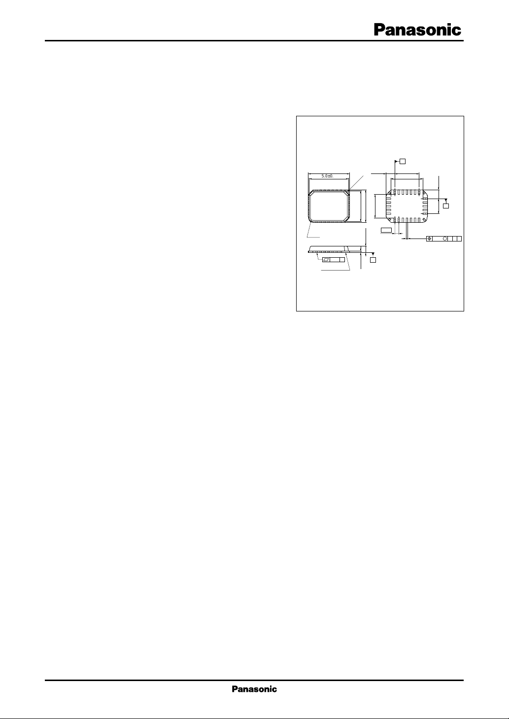
And also, it is housed in an ultrathin, 4-directional-
5.2±0.2 (1.10) 3.0±0.2
5.0±0.1
19 13
20
24
1
R0.3
3-C0.5
12
8
lead SMD-package whose thickness is 0.8 mm maximum
and pin-pitch is 0.5 mm therefore it is most suitable for
making a power supply small and thin.
0.10
Seating plane
■ Features
• Wide operating supply voltage range: 1.8 V to 14 V
• High-precision reference voltage circuit
— V
pin voltage: ±1%
REF
— Error amplifier: ±1.5%
• Ultrathin surface mounting package for miniaturized and thinner power supplies
Package: QFN-24
0.5-mm lead pitch
5.4 mm × 4.4 mm × t 0.8 mm
• Supports control over a wide output frequency range: 20 kHz to 1 MHz
• On/off (sequence control) pins provided for each channel for easy sequence control setup
• The negative supply error amplifier supports 0-volt input.
Common-mode input voltage range: − 0.1 V to V
−1.4 V
CC
This allows the number of external components to be reduced by two resistors.
• Fixed duty factor: 86%
However, the duty can be adjusted to anywhere from 0% to 100% with an external resistor.
• Timer latch short-circuit protection circuit (charge current: 1.1 µA typical)
• Low input voltage malfunction prevention circuit (U.V.L.O.)
(operation start voltage: 1.67 V typical)
• Standby function (active-high control input, standby mode current: 1 µA maximum)
QFN024-P-0405
4.0±0.1
4.2±0.2
0.80max.
0.2±0.1
3.0±0.1
S
A
4.0±0.1
13
12
8
7
0.50
Unit: mm
19
17
0.2±0.1
20
2.0±0.2 (1.10)
24
0.10 SSA B
B
M
■ Applications
• Electronic equipment that requires a power supply system
1
Page 2
AN8049FHN Voltage Regulators
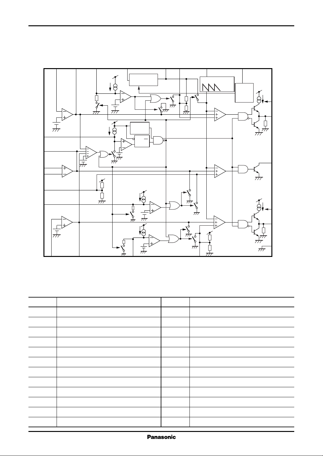
■ Block Diagram
S.C.P.
FB3
IN+3
IN−3
DT3
CTL3
IN-121FB122CTL1
Error
amplifier 1
1.26 V
23
18
S.C.P. comp.
Error
amplifier 2
16
17
24
3
Error
amplifier 3
1.26 V
19
20
V
REF
5
1.1 mA
0.9 V
1.1 mA
20 kΩ
V
CC
50 kΩ50 kΩ
20 kΩ
CC
V
14
Reference voltage
supply
1.26 V
U.V.L.O.
1.26 V
1.1 mA
1.1 mA
20 kΩ
4
7
V
REF
1.26 V
(Allowance: ±1%)
R
Q
S
Latch
1.26 V
1.26 V
REF
V
2
DT1
50 kΩ
OSC
15
Triangular wave generator
50 kΩ
PWM1
PWM3
PWM2
1
0.7 V
0.3 V
V
REF
50 kΩ
50 kΩ
Off
6
On/off
control
V
CC
V
CC
9
RB1
10
OUT1
30 kΩ
13
OUT3
8
RB2
11
OUT2
30 kΩ
12
GND
IN−2
FB2
■ Pin Descriptions
Pin No. Description
1 DT2
2 DT1
3 CTL3
4 CTL2
5 CTL1
6 Off
7V
8 RB2
9 RB1
10 OUT1
11 OUT2
12 GND
2
REF
CTL2
DT2
Pin No. Description
13 OUT3
14 V
CC
15 OSC
16 IN+3
17 IN−3
18 FB3
19 IN−2
20 FB2
21 IN−1
22 FB1
23 S.C.P.
24 DT3
Page 3
Voltage Regulators AN8049FHN
■ Absolute Maximum Ratings
Parameter Symbol Rating Unit
Supply voltage V
Off pin allowable application voltage V
Error amplifier input allowable V
application voltage
*2
OUT1 and OUT2 pin output I
CC
OFF
IN
SO(OUT)
source current
OUT3 pin output current I
Power dissipation
*1
Operating temperature T
Storage temperature T
Note)*1: Ta = 85°C. For the independent IC without a heat sink.
2: When VCC is less than 6 V, V
*
IN−1
SI(OUT)
and V
P
D
opr
stg
must be VCC.
IN+2
14.2 V
14.2 V
V
CC
V
−50 mA
+50 mA
111 mW
−30 to +85 °C
−55 to +150 °C
■ Recommended Operating Range
Parameter Symbol Range Unit
Off pin application voltage V
OUT1 and OUT2 pin output source current I
OUT3 pin output current I
Timing resistance R
Timing capacitance C
Oscillator frequency f
Short-circuit protection time-constant setting capacitance C
Output current setting resistance R
OFF
SO(OUT)
SI(OUT)
T
T
OUT
SCP
B
0 to 14 V
−40 (min.) mA
40 (max.) mA
3 to 33 kW
100 to 1 000 pF
20 to 1 000 kHz
1 000 (min.) pF
750 to 15 000 Ω
3
Page 4
AN8049FHN Voltage Regulators
■ Electrical Characteristics at V
= 2.4 V, C
CC
Parameter Symbol Conditions Min Typ Max Unit
Reference voltage block
Reference voltage V
REFIREF
Line regulation with input fluctuation Line V
Load regulation Load I
V
temperature characteristics V
REF
V
pin short-circuit current I
REF
RFEdTTa
OC
U.V.L.O. block
Circuit operation start voltage V
UON
Error amplifier 1 block
Input threshold voltage 1 V
Input bias current 1 I
High-level output voltage 1 V
Low-level output voltage 1 V
Output source current 1 I
Output sink current 1 I
VTH temperature characteristics 1 V
Open-loop gain 1 A
TH1
B1
EH1
EL1
SO(FB)1
SI(FB)1
THdT1Ta
V1
Error amplifier 2 block
Input threshold voltage 2 V
Input bias current 2 I
High-level output voltage 2 V
Low-level output voltage 2 V
Output source current 2 I
Output sink current 2 I
VTH temperature characteristics 2 V
Open-loop gain 2 A
TH2
B2
EH2
EL2
SO(FB)2
SI(FB)2
THdT2Ta
V2
Error amplifier 3 block
Input offset voltage V
Common-mode input voltage range V
Input bias current 3 I
High-level output voltag 3 V
Low-level output voltage 3 V
Output source current 3 I
Output sink current 3 I
Open-loop gain 3 A
IO
ICR
B3
EH3
EL3
SO(FB)3
SI(FB)3
V3
= 0.1 µF, Ta = 25°C
REF
= − 0.1 mA 1.247 1.26 1.273 V
= 1.8 V to 14 V 220mV
CC
= −0.1 mA to −1 mA −20 −3 mV
REF
= −30°C to +85°C 1 %
−10 mA
1.59 1.67 1.75 V
1.241 1.26 1.279 V
0.1 0.2 µA
1.0 1.2 1.4 V
0.2
−38 −31 −24 µA
0.5 mA
= −30°C to +85°C 1.5 %
80 dB
1.241 1.26 1.279 V
0.1 0.2 µA
1.0 1.2 1.4 V
0.2
−38 −31 −24 µA
0.5 mA
= −30°C to +85°C 1.5 %
80 dB
−6 6mV
− 0.1 V
CC
−1.4
− 0.6 − 0.3 µA
1.0 1.2 1.4 V
0.2
−38 −31 −24 µA
0.5 mA
80 dB
V
4
Page 5
Voltage Regulators AN8049FHN
■ Electrical Characteristics (continued) at V
= 2.4 V, C
CC
= 0.1 µF, Ta = 25°C
REF
Parameter Symbol Conditions Min Typ Max Unit
Oscillator block
Oscillator frequency f
Frequency supply voltage f
RT = 7.5 kΩ, CT = 680 pF 170 190 210 kHz
OUT
RT = 7.5 kΩ, CT = 680 pF 1 %
DV
characteristics
Frequency temperature f
RT = 7.5 kΩ, CT = 680 pF 3 %
DT
characteristics
Output 1 block
Output duty factor 1 Du1RT = 7.5 kΩ, CT = 680 pF 80 86 92 %
High-level output voltage 1 V
Low-level output voltage 1 V
Output source current 1 I
Output sink current 1 I
SO(OUT)1VO
SI(OUT)1VO
Pull-down resistor 1 R
OH1IO
OL1IO
O1
= −10 mA, RB = 1 kΩ VCC −1 V
= 10 mA, RB = 1 kΩ0.2 V
= 0.7 V, RB = 1 kΩ−32 −27 −22 mA
= 0.7 V, RB = 1 kΩ 40 mA
20 30 40 kΩ
Output 2 block
Output duty factor 2 Du2RT = 7.5 kΩ, CT = 680 pF 80 86 92 %
High-level output voltage 2 V
Low-level output voltage 2 V
Output source current 2 I
Output sink current 2 I
SO(OUT)2VO
SI(OUT)2VO
Pull-down resistor 2 R
OH2IO
OL2IO
O2
= −10 mA, RB = 1 kΩ VCC −1 V
= 10 mA, RB = 1 kΩ0.2 V
= 0.7 V, RB = 1 kΩ−32 −27 −22 mA
= 0.7 V, RB = 1 kΩ 40 mA
20 30 40 kΩ
Output 3 block
Output duty factor 3 Du3RT = 7.5 kΩ, CT = 680 pF 80 86 92 %
Output saturation voltage V
O(SAT)
0.2 V
Short-circuit protection circuit block
Input standby voltage V
Input threshold voltage V
Input latch voltage V
Charge current I
Comparator threshold voltage V
STBY
THPC
IN
CHG
THL
V
= 0 V −1.3 −1.0 −0.7 µA
SCP
0.1 V
0.8 0.9 1.0 V
0.1 V
1.26 V
On/off control block
Input threshold voltage V
Off pin current I
ON(TH)
OFF
V
= 5 V 35 µA
OFF
0.7 1.0 1.3 V
CTL block
Input threshold voltage V
Charge current I
THCTL
CTL
V
= 0 V −1.3 −1.0 −0.7 µA
CTL
1.07 1.26 1.47 V
Whole device
Average consumption current I
Standby mode current I
CC(OFF)RB
CC(SB)
= 9.1 kΩ, duty = 50% 4.2 5.5 mA
1 µA
5
Page 6
AN8049FHN Voltage Regulators
■ Terminal Equivalent Circuit
Pin No. Equivalent circuit Description I/O
1 DT2: I
Sets the channel 2 soft start time.
Set the time by connecting a capacitor
7 1520
50 kΩ
1
50 kΩ
PWM2
2 DT1:
227
15
50 kΩ
2
50 kΩ
PWM1
3 CTL3: I
V
CC
20 kΩ
1.1 µA
High
channel 3 operation
1.26 V
is turned off.
3
between this pin and ground.
Note that although the channel 2
maximum on duty is set internally to
86%, the maximum on duty can be set
to a value of 86% or less by inserting
a resistor between this pin and ground,
and can be set to a value of 86% or
more by inserting a resistor between
this pin and the V
REF
pin.
Sets the channel 1 soft start time.
Set the time by connecting a capacitor
between this pin and ground.
Note that although the channel 1
maximum on duty is set internally to
86%, the maximum on duty can be set
to a value of 86% or less by inserting
a resistor between this pin and ground,
and can be set to a value of 86% or
more by inserting a resistor between
this pin and the V
REF
pin.
Controls the on/off state of channel 3.
A delay can be provided in the power
supply turn-on start time by connecting
a capacitor between this pin and ground.
t
= 1.26 (V) × C
DLY3
(µF)/1.1 (µA) (s)
CTL3
This pin can also be used to control the
on/off state with an external signal.
In that case, the allowable input voltage
range is from 0 V to V
. Note that
CC
during U.V.L.O. and timer latch
operation, this pin is connected to
ground through a 20 kΩ resistor.
6
Page 7
Voltage Regulators AN8049FHN
■ Terminal Equivalent Circuit (continued)
Pin No. Equivalent circuit Description I/O
4 CTL2: I
Controls the on/off state of channel 2.
V
CC
20 kΩ
1.1 µA
High
channel 2 operation
1.26 V
is turned off.
4
5 CTL1: I
V
CC
20 kΩ
1.1 µA
High
channel 1 operation
1.26 V
is turned off.
5
6 Off: I
Start and stop of
internal circuits.
6
100 kΩ
7V
V
CC
7
A delay can be provided in the power
supply turn-on start time by connecting
a capacitor between this pin and ground.
t
= 1.26 (V) × C
DLY2
(µF)/1.1 (µA) (s)
CTL2
This pin can also be used to control the
on/off state with an external signal.
In that case, the allowable input voltage
range is from 0 V to V
. Note that
CC
during U.V.L.O. and timer latch
operation, this pin is connected to
ground through a 20 kΩ resistor.
Controls the on/off state of channel 1.
A delay can be provided in the power
supply turn-on start time by connecting
a capacitor between this pin and ground.
t
= 1.26 (V) × C
DLY1
(µF)/1.1 (µA) (s)
CTL1
This pin can also be used to control the
on/off state with an external signal.
In that case, the allowable input voltage
range is from 0 V to V
. Note that
CC
during U.V.L.O. and timer latch
operation, this pin is connected to
ground through a 20 kΩ resistor.
Controls the on/off state.
When the input is high: normal
operation
(V
> 1.2 V)
OFF
When the input is low: standby mode
V
< 0.6 V)
OFF
In standby mode, the total current
consumption is held to under 1 µA.
:O
REF
Outputs the internal reference voltage.
The reference voltage is 1.26 V
(allowance: ±1%) when V
and I
is −0.1 mA. Insert a capacitor
REF
of at least 0.1 µF between V
is 2.4 V
CC
REF
and
ground for phase compensation.
7
Page 8

AN8049FHN Voltage Regulators
■ Terminal Equivalent Circuit (continued)
Pin No. Equivalent circuit Description I/O
8 RB2: I
V
CC
Connection for a resistor that sets the
channel 2 output source current.
Use a resistor in the range 750 Ω to
1.5 kΩ.
11
200 Ω
30 kΩ
8
9 RB1: I
V
CC
Connection for a resistor that sets the
channel 1 output source current.
Use a resistor in the range 750 Ω to
1.5 kΩ.
10
200 Ω
30 kΩ
9
10 OUT1: O
V
9
I
SO(OUT)1
10
CC
Push-pull output.
The absolute maximum rating for the
output source current is −50 mA.
Connecting the external resistor to RB1
terminal allows this circuit to provide
30 kΩ
an output source current with excellent
line regulation and minimal sample-to-
sample variations.
11 OUT2: O
V
8
I
SO(OUT)2
11
CC
Push-pull output.
The absolute maximum rating for the
output source current is −50 mA.
Connecting the external resistor to RB2
terminal allows this circuit to provide
30 kΩ
an output source current with excellent
line regulation and minimal sample-to-
sample variations.
12 GND:
Ground.
12
8
Page 9

Voltage Regulators AN8049FHN
■ Terminal Equivalent Circuit (continued)
Pin No. Equivalent circuit Description I/O
13 OUT3: O
14 VCC:
15 OSC: O
V
CC
0.2 V
15
16 IN+3: I
V
CC
17 IN−3: I
1.5 kΩ 1.5 kΩ
14
13
Latch
S
R
V
CC
Open-collector output.
The absolute maximum rating for the
output current is +50 mA.
Power supply terminal.
Provide the operating supply voltage
in the range 1.8 V to 14 V.
Connection for the capacitor and
resistor that determine the oscillator
frequency. Use a capacitor in the range
Q
100 pF to 1 000 pF and a resistor in
the range 3 kΩ to 33 kΩ. Use an
oscillator frequency in the range
20 kHz to 1 MHz.
Noninverting input to the error
amplifier 3.
1617
Inverting input to the error amplifier 3.
18 FB3: O
16
17
7
31 µA
OSC
PWM3
Output from the error amplifier 3.
This circuit can provide a source
current of −31 µA or a sink current of
0.5 mA (minimum).
0.5 mA
min.
18
19 IN−2: I
19
14
1.5 kΩ
Inverting input to the error amplifier 2.
1.26 V
9
Page 10

AN8049FHN Voltage Regulators
■ Terminal Equivalent Circuit (continued)
Pin No. Equivalent circuit Description I/O
V
19
21
CC
1.26 V
14
1.5 kΩ
31 µA
OSC
0.5 mA
min.
20
1.26 V
PWM2
Output from the error amplifier 2.
This circuit can provide a source
current of −31 µA or a sink current of
0.5 mA (minimum).
Inverting input to the error amplifier 1.
20 FB2: O
21 IN−1: I
22 FB1: O
21
V
CC
31 µA
OSC
PWM1
Output from the error amplifier 1.
This circuit can provide a source
current of −31 µA or a sink current of
0.5 mA (minimum).
1.26 V
0.5 mA
min.
22
23 S.C.P.: O
V
CC
Connection for the capacitor that sets
the timer latch short-circuit protection
1.5 kΩ
1.1 µA
23
1.26 V
Latch
S
R
Q
Output
shutoff
circuit time constant. Use a capacitor
with a value of 1 000 pF or higher.
The charge current I
is 1.1 µA
CHG
typical.
24 DT3: I
Sets the channel 3 soft start time.
Set the time by connecting a capacitor
7
18 15
between this pin and ground. Note that
although the channel 3 maximum on duty
50 kΩ
24
50 kΩ
PWM3
is set internally to 86%, the maximum
on duty can be set to a value of 86% or
less by inserting a resistor between this
pin and ground, and can be set to a value
of 86% or more by inserting a resistor
between this pin and the V
REF
pin.
10
Page 11

Voltage Regulators AN8049FHN
■ Usage Notes
[1] Allowable power dissipation
Since the power dissipation (P) in this IC increases proportionally with the supply voltage, applications must be
careful to operate so that the loss does not exceed the allowable power dissipation, P
Reference formula:
P = (V
<P
CC−VBEQ1
+(V
+V
+V
D
V
BEQ1
I
SO(OUT)1
Du
V
BEQ2
I
SO(OUT)2
Du
V
O(SAT)3
I
OUT3
Du
I
CC
CC−VBEQ2
O(SAT)3
× I
CC
CC
1
2
3
) × I
× I
) × I
OUT3
SO(OUT)1
SO(OUT)2
× Du
× Du
× Du
3
1
← Power dissipation in the channel 1 output stage
← Power dissipation in the channel 2 output stage
2
← Power dissipation in the channel 3 output stage
← Power dissipation between VCC and ground
: The voltage between the base and emitter of the npn transistor Q1
: The OUT1 pin output source current
(When R
is 1 kΩ, I
RB1
will be 38 mA, maximum.)
SO(OUT)1
: The output 1 duty factor
: The voltage between the base and emitter of the npn transistor Q2
: The OUT2 pin output source current
(When R
is 1 kΩ, I
RB2
will be 38 mA, maximum.)
SO(OUT)2
: The output 2 duty factor
: The OUT3 pin saturation voltage (0.5 V maximum when OUT1 is 40 mA.)
: The OUT3 pin current (This will be {VCC − V
BEQ3
− V
: The output 3 duty factor
: The VCC pin current
, for the package.
D
}/RO3.)
O(SAT)3
[2] Allowable V
CC
ripple
VCC ripple due to the switching transistor being turned on and off can cause this IC's U.V.L.O. circuit, which is
biased by VCC, to operate incorrectly, and can cause the S.C.P. capacitor charging operation to fail to start when the
output is shorted.
The figure shows the allowable range for V
either by inserting a ripple filter in the V
ripple. Applications should reduce VCC ripple to be within this range,
CC
line or by inserting a capacitor between the IC GND and VCC pins and
CC
locating that capacitor as close to the IC as possible.
Note that the allowable range shown here is the result of testing the IC alone and that the allowable range may
differ depending on the actual structure of the power supply circuit. Also note that this allowable range is a design
target, and is not guaranteed by testing of all samples.
Allowable V
10 M
Allowable range
is 3 V.
when V
1 M
100 k
Ripple frequency (Hz)
10 k
012345678
CC
VCC ripple voltage VCC(AC) (V[p-p])
ripple
CC
Allowable range
is 10 V.
when V
CC
11
Page 12

AN8049FHN Voltage Regulators
■ Application Notes
[1] QFN024-P-0405 package power dissipation
T
P
D
a
1.200
1.075
1.000
0.800
(W)
D
0.660
0.600
0.400
Power dissipation P
0.279
0.200
Independent IC
without a heat sink
R
= 357.4°C/W
th(j−a)
0.000
0 25 50 75 85 100 125
When mounted on a 4-layer printed
circuit board (50×50×t0.8 mm
= 93.0°C/W
R
th(j−a)
When mounted on a standard
printed circuit board
(glass epoxy: 50×50×t0.8 mm
R
= 151.5°C/W
th(j−a)
Ambient temperature Ta (°C)
3
)
3
)
12
Page 13

Voltage Regulators AN8049FHN
■ Application Notes (continued)
[2] Main characteristics
f
Maximum output duty
Timing capacitance Oscillator frequency
1M
RT = 3 kΩ
(Hz)
100k
OUT
f
10k
10p 1n 10n
CT (F)
RT = 7.5 kΩ
RT = 33 kΩ
(%)
3
, Du
2
, Du
1
Du
OSC
(R
= 3 kΩ)
95
90
85
80
75
T
Du
3
Du1 , Du
2
1M100k10k
(Hz)
f
OSC
(%)
3
, Du
2
, Du
1
Du
(mA)
SO(OUT)
I
−10
−20
−30
−40
−50
−60
−70
−80
95
90
85
80
75
0
Maximum output duty
f
OSC
= 7.5 kΩ)
(R
T
f
(Hz)
OSC
RB I
SO(OUT)
VCC = 1.8 V
2.4 V
8 V
14 V
(Ω)
R
B
Du1 , Du
f
Maximum output duty
OSC
= 33 kΩ)
(R
Du
2
RB I
T
f
OSC
R
B
1M100k10k
(Hz)
SI(OUT)
VCC = 14 V
8 V
1.8 V, 2.4 V
100k10k1k100
(Ω)
95
Du
90
3
Du
(%)
3
Du
3
2
1M100k10k
100k10k1k100
, Du
2
, Du
1
Du
(mA)
SI(OUT)
I
1
85
80
75
100
90
80
70
60
50
40
30
20
10
0
13
Page 14

AN8049FHN Voltage Regulators
■ Application Notes (continued)
[3] Timing charts
pin voltage
V
CC
waveform
1.67 V
Output short
S.C.P. pin
voltage
waveform
CTL pin
voltage
waveform
1.26 V
FB
1.26 V
DT
OSC
0.9 V
OUT1/2 pin voltage waveform
Totem pole circuit
output (Step-up output)
OUT3 pin voltage waveform
Open-collector output
(Inverting or step-down output)
14
Page 15

Voltage Regulators AN8049FHN
■ Application Notes (continued)
[4] Function descriptions
1. Reference voltage block
This circuit is composed of a band gap circuit, and outputs a 1.26 V (typical) reference voltage that is
temperature compensated to a precision of ±1%. This reference voltage is stabilized when the supply voltage is 1.8
V or higher. This reference voltage is used by error amplifiers 1 and 2.
2. Triangular wave generator
This circuit generates a triangular wave like a
sawtooth with a peak of 0.7 V and a trough of 0.2 V
using a capacitor CT (for the time constant) and resistor
R
connected to the OSC pin (pin 15). The oscillator
T
frequency can be set to an arbitrary value by selecting
appropriate values for the external capacitor and resistor, C
and RT. This IC can use an oscillator frequency
T
in the range 20 kHz to 1 MHz. The triangular wave
signal is provided to the noninverting input of the PWM
comparator in each channel internally to the IC. Use
the formulas below for rough calculation of the oscillator frequency.
Rapid charge
Figure 1. Triangular oscillator waveform
t
1
t
2
Discharge
T
V
OSCH
0.7 V
V
OSCL
0.2 V
f
OSC
≈ −
× RT × ln
C
T
1
V
V
≈ 0.8 ×
OSCL
OSCH
1
CT × R
(Hz)
T
Note, however, that the above formulas do not take the rapid charge time, overshoot, and undershoot into
account. See the experimentally determined graph of the oscillator frequency vs. timing capacitance value provided in the main characteristics section.
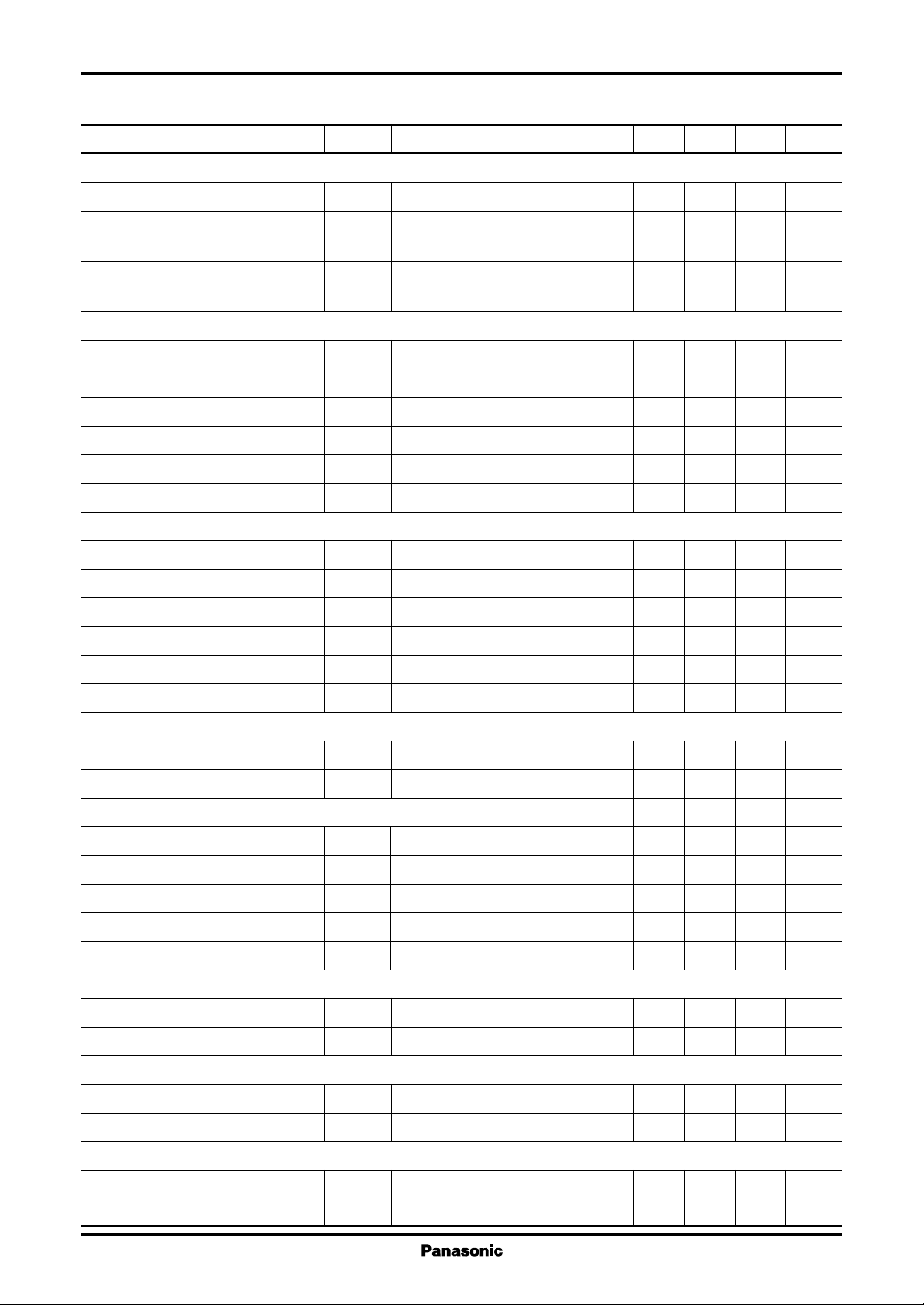
3. Error amplifier 1
This circuit is an npn-transistor input error amplifier
that detects and amplifies the DC-DC converter output
voltage, and inputs that signal to a PWM comparator.
The 1.26 V internal reference voltage is applied to the
noninverting input. Arbitrary gain and phase compensation can be set up by inserting a resistor and capacitor
in series between the FB1 pin (pin 22) and the IN±1 pin
(pin 21). The output voltage V
can be set using the
OUT1
circuit shown in the figure.
R1
R2
V
OUT1
V
FB1
IN−1
OUT1
22
Error
amplifier 1
21
= 1.26 ×
1.26 V
R
+
1
R
To the PWM
comparator input
R
2
2
Figure 2. Connection method of error amplifier 1
(Step-up output)
15
Page 16

AN8049FHN Voltage Regulators
■ Application Notes (continued)
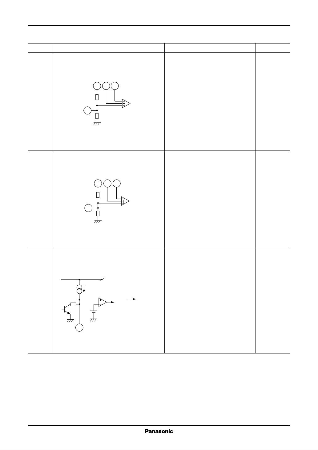
[4] Function descriptions (continued)
V
FB2
IN−2
OUT2
20
Error
amplifier 2
19
= 1.26 ×
1.26 V
R
+
1
R
To the PWN
comparator input
R
2
2
4. Error amplifier 2
This circuit is an npn-transistor input error
amplifier that detects and amplifies the DC-DC
converter output voltage, and inputs that signal to
a PWM comparator. The 1.26 V internal reference
R1
V
OUT2
voltage is applied to the noninverting input. Arbitrary gain and phase compensation can be set up
by inserting a resistor and capacitor in series between the FB2 pin (pin 20) and the IN−2 pin (pin
19). The output voltage V
can be set using the
OUT2
R2
circuit shown in the figure.
Figure 3. Connection method of error amplifier 2 (Step-up output)
5. Error amplifier 3
This circuit is a pnp-transistor input error amplifier that detects and amplifies the DC-DC converter output
voltage and inputs that signal to a PWM comparator. Arbitrary gain and phase compensation can be set up by
inserting a resistor and capacitor in series between the FB3 pin (pin 18) and the IN−3 pin (pin 17). The output voltage
V
can be set using the circuit shown in the figure.
OUT3
Step-down output Inverting output
R1
R2
FB3
18
V
V
OUT3
REF
V
R3
R4
OUT3
=
R
R
2
1+R2
IN−3
IN+3
×
Error
amplifier 3
16
17
R
R
+
3
4
R
4
× V
To the PWM
comparator input
REF
R1
R2
V
V
REF
OUT3
V
FB3
OUT3
IN+3
IN−3
= −V
18
Error
amplifier 3
16
17
REF
×
To the PWM
comparator input
R
2
R
1
Figure 4. Connection method of error amplifier 3
6. Timer latch short-circuit protection circuit
This circuit protects the external main switching elements, flywheel diodes, choke coils, and other components
against degradation or destruction if an excessive load or a short circuit of the power supply output continues for
longer than a certain fixed period.
The timer latch short-circuit protection circuit detects the output of the error amplifiers. If the DC-DC converter
output voltage drops and an FB pin (pins 18, 20, or 22) voltage exceeds 0.9 V, the S.C.P. comparator outputs a low
level and the timer circuit starts. This starts charging the external protection circuit delay time capacitor.
If the error amplifier output does not return to the normal voltage range before that capacitor reaches 1.26 V,
the latch circuit latches, the output drive transistors are turned off, and the dead-time is set to 100%.
16
Page 17

Voltage Regulators AN8049FHN
■ Application Notes (continued)
[4] Function descriptions (continued)
7. Low input voltage malfunction prevention circuit (U.V.L.O.)
This circuit protects the system against degradation or destruction due to incorrect control operation when the
power supply voltage falls during power on or power off.
The low input voltage malfunction prevention circuit detects the internal reference voltage that changes with
the supply voltage level. While the supply voltage is rising, this circuit cuts off the output drive transistor until the
reference voltage reaches 1.67 V. It also sets the dead-time to 100% and at the same time holds the S.C.P. pin (pin
23) and the DT pins (pins 1, 2, and 24) at 0 V, and the OSC pin (pin 15) at about 1.2 V.
8. PWM comparators
The PWM comparators control the on-period of the output pulse according to their input voltage.
The output transistors are turned on during periods when the OSC pin (pin 15) triangular wave is lower than
both of the corresponding FB pin (pins 18, 20, or 22) and the corresponding DT pin (pins 1, 2, or 24).
The PWM 2 circuit turns the output transistor on during periods when OSC pin (pin 15) triangular wave is at
a higher level than both of the FB2 pin (pin 20) and the DT2 pin (pin 1).
The maximum duty is set to 86% internally, but it can be set to a value lower than 86% by inserting a resistor
between the corresponding DT pin and ground, and can be set to a value higher than 86% by inserting a resistor
between the corresponding DT pin and the V
The IC's soft start function operates to gradually increase the width of the output pulse on-period during startup
if a capacitor is inserted between the DT pin and ground.
REF
pin.
9. Output 1 and output 2 blocks
These output circuits have a totem pole structure. A constant-current source output with good line regulation
can be set up freely by connecting current setting resistors to the RB pins.
These circuits can provide a constant-current source output of up to 50 mA.
10. Output 3 block
This output circuit has an open collector structure.
An output current of up to 50 mA can be provided, and the output pin has a breakdown voltage of 15 V.
11. CTL block
The CTL block output circuit also has a totem pole structure. A constant-current source output with good line
regulation can be set up freely by connecting current setting resistors to the RB2 pin.
The CTL block can provide a constant-current source output of up to 50 mA.
17
Page 18

AN8049FHN Voltage Regulators
■ Application Notes (continued)
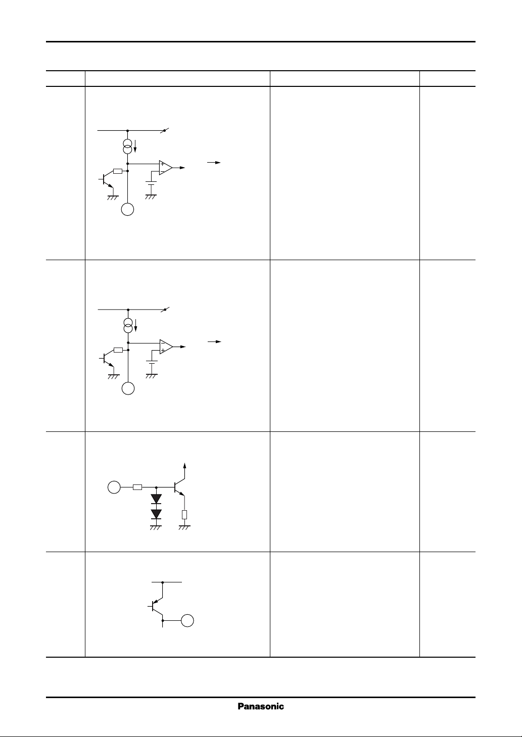
[5] Time constant setup for the timer latch short-circuit protection circuit
Figure 6 shows the structure of the timer latch short-circuit protection circuit. The short-circuit protection
comparator continuously compares a 0.9 V reference voltage with the FB1, FB2, and FB3 error amplifier outputs.
When the DC-DC converter output load conditions are stable, the short-circuit protection comparator holds its
average value since there are no fluctuations in the error amplifier outputs. At this time, the output transistor Q1 will
be in the conducting state, and the S.C.P. pin will be held at 0 V.
If the output load conditions change rapidly and a high-level signal (0.9 V or higher) is input to the short-circuit
protection comparator from the error amplifier output, the short-circuit protection comparator will output a low level
and the output transistor Q1 will shut off. Then, the capacitor C
When the external capacitor C
is charged to about 1.26 V by the constant current of about 1.1 mA, the latch circuit
SCP
will latch and the dead-time will be set to 100% with the output held fixed at the low level. Once the latch circuit has
latched, the S.C.P. pin capacitor will be discharged to about 0 V, but the latch circuit will not reset unless either power
is turned off or the power supply is restarted using on/off control.
t
1.26 V = I
∴tPE (s) = 1.15 × C
CHG
PE
×
C
SCP
(µF)
SCP
connected to the S.C.P. pin will start to charge.
SCP
(V)
V
SCP
At power supply startup, the output appears to be
in the shorted state, and the IC starts to charge the
S.C.P. pin capacitor. Therefore, users must select an
external capacitor that allows the DC-DC converter
output voltage to rise before the latch circuit in the
later stage latches. In particular, care is required if the
soft start function is used, since that function makes
the startup time longer.
FB1
FB2
FB3
22
20
18
On/off control
S.C.P. comp.
0.9 V
Q1
V
CC
Short-circuit detection time t
1.26
0
Figure 5. S.C.P. pin charging waveform
V
REF
U.V.L.O.
1.1 µA
Latch
R
S
Q
High level detection comparator
1.26 V
PE
t (s)
Output shutoff
18
23
S.C.P.
Figure 6. Short-circuit protection circuit
Page 19

Voltage Regulators AN8049FHN
■ Application Notes (continued)
[6] Parallel synchronous operation of multiple ICs
Multiple instances of this IC can be operated in parallel. If the OSC pins (pin 15) and Off pins (pin 6) are connected
to each other as shown in figure 7, the ICs will operate at the same frequency.
It is also possible to operate a one-channel control IC (e.g. the AN8016SH or AN8016NSH) and a two-channel
control IC (e.g. the AN8017SA or AN8018SA) in this parallel synchronous mode. In this case, short the OSC and Off
pins together.
Note that it is not possible to control the on/off states of each IC operating in this mode independently. It is only
possible to turn all the ICs on or off at the same time remotely.
OSC pins
connected
together
S.C.P.
OSC
15
AN8049FHN AN8049FHN
2
7
6
Off
H
REF
V
S.C.P.
2
L
Figure 7. Slave operation circuit example
Off pins
connected
together
15
OSC
6
Off
7
REF
V
19
Page 20

AN8049FHN Voltage Regulators
■ Application Notes (continued)
[7] Sequential operation
Delays can be provided in the startup times by inserting capacitors (C
Delay time: t
= 1.26 (V) × C
DLY
(µF)/1.1 (µA) (s)
CTL
Note that the individual channels can also be turned on or off independently by external signals. These external
signals may have voltages in the range 0 V to V
CC
.
) between the CTL pins and ground.
CTL
C
CTL3
C
CTL1
AN8049FHN
3
4
CTL3
CTL2
C
CTL2
< C
CTL2
< C
5
CTL1
CTL3
C
CTL1 CTL2 CTL3
1.26 V
U.V.L.O. cleared
CTL1
OUT1
OUT2
OUT3
20
Figure 8. Sequential operation
Page 21

Voltage Regulators AN8049FHN
■ Application Notes (continued)
[8] Differences between this IC and the AN8049SH
The pin arrangements differ. The AN8049SH is an alternative package version of this IC.
AN8049FHN
AN8049SH
FB2
IN−1
FB1
S.C.P.
DT3
20
21
22
23
24
1
19
IN−2
DT2
18
2
FB3
DT1
IN−3
17
3
CTL3
16
4
IN+3
CTL2
OSC
15
5
CTL1
14
6
CC
OUT3
V
13
12
GND
11
OUT2
10
OUT1
9
RB1
8
RB2
7
Off
REF
V
24
1
FB1
S.C.P.
23
2
IN−1
DT3
22
3
FB2
DT2
21
4
IN−2
DT1
FB3
20
5
CTL3
19
6
IN−3
CTL2
IN+3
18
7
CTL1
OSC
17
8
Off
VCCOUT3
16
15
9
10
REF
RB2
V
14
11
GND
RB1
OUT2
13
12
OUT1
21
Page 22

AN8049FHN Voltage Regulators
■ Application Notes (continued)
[9] Error amplifier frequency characteristics
1. Error amplifiers 1 and 2
(Test circuit)
V
IN
4 mV[
P-P]
100 kΩ
2.3 V
2. Error amplifier 3
(dB)
Gain
-10
-20
180
135
(°)
Phase
−45
40
30
20
10
0
90
45
0
100M100k 1M 10M10k1k
Frequency (Hz)
100 kΩ
1 kΩ10 µF
IN−1
Amp.1
V
REF
FB1
V
OUT
1.26 V
(Test circuit)
10 µF
V
IN
4 mV[p-p]
1 V
1 kΩ
IN−3
1 kW
IN+3
1 kΩ
Amp.3
100 kΩ
10 µF
FB3
V
OUT
(dB)
Gain
−10
−20
−45
−90
(°)
−135
Phase
−180
−225
40
30
20
10
0
0
100M100k 1M 10M10k1k
Frequency (Hz)
22
Page 23

Voltage Regulators AN8049FHN
■ Application Circuit Example
IN
V
FB2
IN−1
FB1
S.C.P.
DT3
20
21
22
23
24
IN−2
19
1
DT2
FB3
18
2
DT1
IN−3
17
3
CTL3
IN+3
16
4
CTL2
OSC
15
5
CTL1
REF
−
V
O3
+
V
O1
Q3
CC
OUT3
V
14
13
12
GND
V
Q2
11
OUT2
10
OUT1
9
8
6
7
Off
REF
V
RB1
RB2
Q1
+
V
O1
23
 Loading...